 | –≠–ª–µ–∫—Ç—Ä–æ–Ω–Ω—ã–π –∫–æ–º–ø–æ–Ω–µ–Ω—Ç: TB5D1MDR | –°–∫–∞—á–∞—Ç—å:  PDF PDF  ZIP ZIP |
www.ti.com
FEATURES
DESCRIPTION
APPLICATIONS
AI
BI
GND
E1
VCC
DI
E2
CI
AO
BO
CO
DO
9
10
16
15
14
13
12
11
1
2
3
4
5
6
7
8
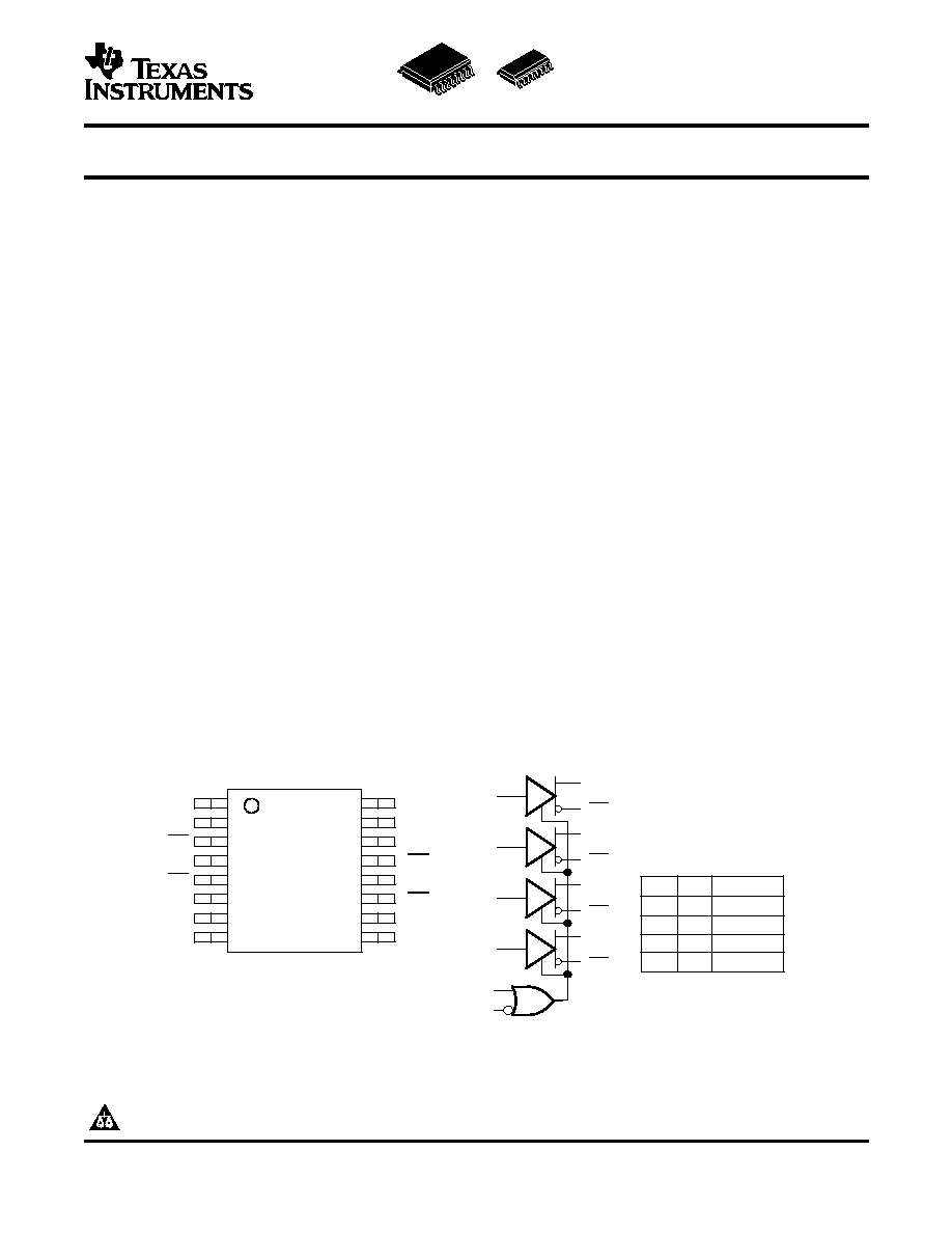
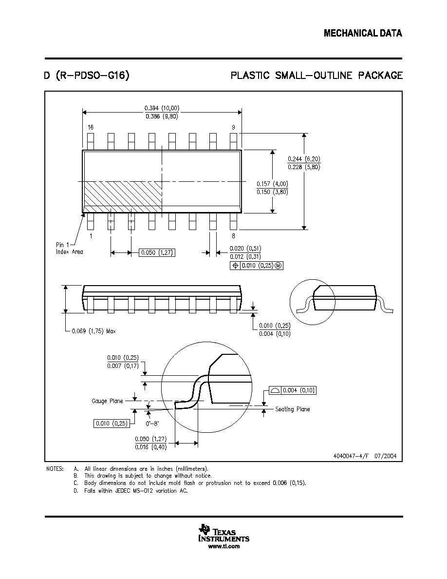
DW AND D PACKAGE
(TOP VIEW)
CO
DO
BO
AO
AI
BI
CI
DI
E1
E2
AO
AO
BO
BO
CO
CO
DO
DO
FUNCTIONAL DIAGRAM
E1
E2 Condition
0
0
Active
1
0
Active
0
1
Disabled
1
1
Active
ENABLE TRUTH TABLE
TB5D1M, TB5D2H
SLLS579B ≠ SEPTEMBER 2003 ≠ REVISED MAY 2004
QUAD DIFFERENTIAL PECL DRIVERS
∑
Functional Replacements for the Agere
These quad differential drivers are TTL input to
BDG1A, BPNGA and BDGLA
pseudo-ECL differential output used for digital data
transmission over balanced transmission lines.
∑
Pin-Equivalent to the General-Trade 26LS31
Device
The TB5D1M device is a pin and functional replace-
ment for the Agere systems BDG1A and BPNGA
∑
2.0 ns Maximum Propagation Delays
quad differential drivers. The TB5D1M has a built-in
∑
0.15 ns Output Skew Typical Between
±
Pairs
lightning protection circuit to absorb large transitions
∑
Capable of Driving 50-
Loads
on the transmission lines without destroying the
∑
5.0-V or 3.3-V Supply Operation
device. When the circuit is powered down it loads the
transmission line, because of the protection circuit.
∑
TB5D1M Includes Surge Protection on
Differential Outputs
The TB5D2H device is a pin and functional replace-
ment for the Agere systems BDG1A and BDGLA
∑
TB5D2H No Line Loading When V
CC
= 0
quad differential drivers. Upon power down the
∑
Third State Output Capability
TB5D2H output circuit appears as an open circuit and
∑
-40
∞
C to 85
∞
C Operating Temp Range
does not load the transmission line.
∑
ESD Protection HBM > 3 kV and CDM > 2 kV
Both drivers feature a 3-state output with a third-state
∑
Available in Gull-Wing SOIC (JEDEC MS-013,
level of less than 0.1 V.
DW) and SOIC (D) Packages
The packaging options available for these quad
differential
line
drivers
include
a
16-pin
SOIC
gull-wing (DW) and a 16-pin SOIC (D) package.
∑
Digital Data or Clock Transmission Over
Both drivers are characterized for operation from
Balanced Transmission Lines
-40
∞
C to 85
∞
C
The logic inputs of this device include internal pull-up
resistors of approximately 40 k
that are connected
to V
CC
to ensure a logical high level input if the inputs
are open circuited.
Please be aware that an important notice concerning availability, standard warranty, and use in critical applications of Texas
Instruments semiconductor products and disclaimers thereto appears at the end of this data sheet.
PRODUCTION DATA information is current as of publication date.
Copyright © 2003≠2004, Texas Instruments Incorporated
Products conform to specifications per the terms of the Texas
Instruments standard warranty. Production processing does not
necessarily include testing of all parameters.

www.ti.com
PACKAGE DISSIPATION RATINGS
THERMAL CHARACTERISTICS
ABSOLUTE MAXIMUM RATINGS
TB5D1M, TB5D2H
SLLS579B ≠ SEPTEMBER 2003 ≠ REVISED MAY 2004
These devices have limited built-in ESD protection. The leads should be shorted together or the device placed in conductive foam
during storage or handling to prevent electrostatic damage to the MOS gates.
ORDERING INFORMATION
PART NUMBER
PART MARKING
PACKAGE
LEAD FINISH
STATUS
TB5D1MDW
TB5D1M
Gull-wing SOIC
NiPdAu
Production
TB5D1MD
TB5D1M
SOIC
NiPdAu
Production
TB5D2HDW
TB5D2H
Gull-wing SOIC
NiPdAu
Production
TB5D2HD
TB5D2H
SOIC
NiPdAu
Production
TB5D1MLDW
TB5D1ML
Gull-wing SOIC
SnPb
Production
TB5D1MLD
TB5D1ML
SOIC
SnPb
Production
TB5D2HLDW
TB5D2HL
Gull-wing SOIC
SnPb
Production
TB5D2HLD
TB5D2HL
SOIC
SnPb
Production
CIRCUIT
T
A
25
∞
C
THERMAL RESISTANCE,
DERATING FACTOR
(1)
T
A
= 85
∞
C POWER
PACKAGE
BOARD
POWER
JUNCTION-TO-AMBIENT
ABOVE T
A
= 25
∞
C
RATING
MODEL
RATING
WITH NO AIR FLOW
Low-K
(2)
754 mW
132.6
∞
C/W
7.54 mW/
∞
C
301 mW
D
High-K
(3)
1166 mW
85.8
∞
C/W
11.7 mW/
∞
C
466 mW
Low-K
(2)
816 mW
122.5
∞
C/W
8.17 mW/
∞
C
326 mW
DW
High-K
(3)
1206 mW
82.9
∞
C/W
12.1 mW/
∞
C
482 mW
(1)
This is the inverse of the junction-to-ambient thermal resistance when board-mounted with no air flow.
(2)
In accordance with the low-K thermal metric definitions of EIA/JESD51-3.
(3)
In accordance with the high-K thermal metric definitions of EIA/JESD51-7.
PARAMETER
PACKAGE
VALUE
UNITS
D
51.4
∞
C/W
JB
Junction-to-board thermal resistance
DW
56.6
∞
C/W
D
45.7
∞
C/W
JC
Junction-to-case thermal resistance
DW
49.2
∞
C/W
over operating free-air temperature range unless otherwise noted
(1)
TB5D1M, TB5D2H
Supply voltage, V
CC
0 V to 6 V
Input voltage
- 0.3 V to (V
CC
+ 0.3 V)
Human Body Model
(2)
All Pins
±
3 kV
ESD
Charged-Device Model
(3)
All Pins
±
2 kV
Continuous power dissipation
See Dissipation Rating Table
Storage temperature, T
stg
-65
∞
C to 130
∞
C
Junction temperature, T
J
130
∞
C
D Package
-80 V to 100 V
Lightning surge, TB5D1M only, see Figure 6
DW Package
-100 V to 100 V
(1)
Stresses beyond those listed under absolute maximum ratings may cause permanent damage to the device. These are stress ratings
only, and functional operation of the device at these or any other conditions beyond those indicated under recommended operating
conditions is not implied. Exposure to absolute-maximum-rated conditions for extended periods may affect device reliability.
(2)
Tested in accordance with JEDEC Standard 22, Test Method A114-A.
(3)
Tested in accordance with JEDEC Standard 22, Test Method C101.
2
www.ti.com
RECOMMENDED OPERATING CONDITIONS
(1)
ELECTRICAL CHARACTERISTICS
TB5D1M, TB5D2H
SLLS579B ≠ SEPTEMBER 2003 ≠ REVISED MAY 2004
MIN
NOM
MAX
UNIT
Supply voltage, V
CC
5.0-V nominal supply
4.5
5
5.5
V
3.3-V nominal supply
3.0
3.3
3.6
V
Operating free-air temperature, T
A
-40
85
∞
C
(1)
The algebraic convention, in which the least positive (most negative) limit is designated as minimum is used in this data sheet, unless
otherwise stated.
over recommended operating conditions unless otherwise noted
parameter
test conditions
min
typ
(1)
max
unit
V
CC
= 4.5 V to 5.5 V,
40
no loads
I
CC
Supply current
mA
V
CC
= 3.0 V to 3.6 V,
40
no loads
V
CC
= 4.5 V to 5.5 V,
290
360
Figure 3 loads all outputs
P
D
Power dissipation
mW
V
CC
= 3.0 V to 3.6 V,
280
360
Figure 4 loads all outputs
V
OH
Output high voltage
V
CC
- 1.8
V
CC
- 1.3
V
CC
- 0.8
V
V
CC
= 4.5 V to 5.5 V,
V
OL
Output low voltage
V
OH
- 1.4
V
OH
- 1.2
V
OH
- 0.7
V
Figure 3
V
OD
Differential output voltage |V
OH
- V
OL
|
0.7
1.2
1.4
V
V
OH
Output high voltage
V
CC
- 1.8
V
CC
- 1.3
V
CC
- 0.8
V
V
CC
= 3.0 V to 3.6 V,
V
OL
Output low voltage
V
OH
- 1.4
V
OH
- 1.1
V
OH
- 0.5
V
Figure 4
V
OD
Differential output voltage |V
OH
- V
OL
|
0.5
1.1
1.4
V
Peak-to-peak common-mode output
V
OC(PP)
C
L
= 5 pF, Figure 5
230
600
mV
voltage
V
OZ
Third-state output voltage
Figure 3 or Figure 4 load
0.1
V
V
IL
Low level input voltage
(2)
0.8
V
V
IH
High level input voltage
2
V
V
IK
Enable input clamp voltage
V
CC
= 4.5 V, I
I
= -5 mA
-1
(3)
V
V
CC
= 5.5 V, V
O
= 0 V
-250
(3)
I
OS
Output short-circuit current
(4)
mA
V
CC
= 5.5 V, V
OD
= 0 V
±
10
(3)
I
IL
Input low current, enable or data
V
CC
= 5.5 V, V
I
= 0.4 V
-400
(3)
µA
Input high current, enable or data
V
CC
= 5.5 V, V
I
=2.7 V
20
µA
I
IH
Input reverse current, enable or data
V
CC
= 5.5 V, V
I
=5.5 V
100
µA
C
IN
Input capacitance
5
pF
(1)
All typical values are at 25
∞
C and with a 3.3-V or 5-V supply.
(2)
The input level provides no noise immunity and should be tested only in a static, noise-free environment.
(3)
This parameter is listed using a magnitude and polarity/direction convention, rather than an algebraic convention, to match the original
Agere data sheet.
(4)
Test must be performed one output at a time to prevent damage to the device. No test circuit attached.
3
www.ti.com
SWITCHING CHARACTERISTICS, 5-V NOMINAL SUPPLY
TB5D1M, TB5D2H
SLLS579B ≠ SEPTEMBER 2003 ≠ REVISED MAY 2004
THIRD STATE--A TB5D1M (or TB5D2H) driver produces pseudo-ECL levels, and has a third-state mode, which
is different than a conventional TTL device. When a TB5D1M (or TB5D2H) driver is placed in the third state, the
base of the output transistors is pulled low, bringing the outputs below the active-low level of standard PECL
devices. [For example: The TB5D1M low output level is typically 2.7 V, while the third state output level is less
than 0.1 V.] In a bidirectional, multipoint, bus application, the driver of one device, which is in its third state, may
be back driven by another driver on the bus whose voltage in the low state is lower than the third-stated device.
This could come about due to differences in the driver's independent power supplies. In this case, the device in
the third state controls the line, thus clamping the line and reducing the signal swing. If the difference voltage
between the independent driver power supplies is small, this consideration can be ignored. Again using the
TB5D1M driver as an example, a typical supply voltage difference between separate drivers of > 2 V can exist
without significantly affecting the amplitude of the signal.
over recommended operating conditions unless otherwise noted
parameter
test conditions
min
typ
(1)
max
unit
t
P1
Propagation delay time, input high to output
(2)
1.2
2
C
L
= 5 pF, See Figure 1 and
ns
Figure 3
t
P2
Propagation delay time, input low to output
(2)
1.2
2
t
P
Capacitive delay
0.01
0.03
ns/pF
Propagation delay time,
t
PHZ
7
12
high-level-to-high-impedance output
Propagation delay time,
t
PLZ
7
12
low-level-to-high-impedance output
C
L
= 5 pF, See Figure 2 and
ns
Figure 3
Propagation delay time,
t
PZH
5
12
high-impedance-to-high-level output
Propagation delay time,
t
PZL
4
12
high-impedance-to-low-level output
t
skew1
Output skew, |t
P1
- t
P2
|
0.15
0.3
t
shew2
Output skew, |t
PHH
- t
PHL
|, |t
PLH
- t
PLL
|
0.15
1.1
C
L
= 5 pF, See Figure 1 and
ns
Figure 3
t
skew(pp)
Part-to-part skew
(3)
0.1
1
t
skew
Output skew, difference between drivers
(4)
0.3
t
TLH
Rise time (20% - 80%)
0.7
2
C
L
= 5 pF, See Figure 1 and
ns
Figure 3
t
THL
Fall time (80% - 20%)
0.7
2
(1)
All typical values are at 25
∞
C and with a 5-V supply.
(2)
Parameters t
P1
and t
P2
are measured from the 1.5 V point of the input to the crossover point of the outputs (see Figure 1).
(3)
t
skew(pp)
is the magnitude of the difference in differential propagation delay times, t
P1
or t
P2
, between any specified outputs of two devices
when both devices operate with the same supply voltage, at the same temperature, and have identical packages and test circuits.
(4)
t
skew
is the magnitude of the difference in differential skew t
skew1
between any specified outputs of a single device.
4
www.ti.com
SWITCHING CHARACTERISTICS, 3.3-V NOMINAL SUPPLY
TB5D1M, TB5D2H
SLLS579B ≠ SEPTEMBER 2003 ≠ REVISED MAY 2004
over recommended operating conditions unless otherwise noted
typ
(1
parameter
test conditions
min
max
unit
)
t
P1
Propagation delay time, input high to output
(2)
1.2
3.5
C
L
= 5 pF, See Figure 1 and
ns
Figure 4
t
P2
Propagation delay time, input low to output
(2)
1.2
3.5
t
P
Capacitive delay
0.01
0.03
ns/pF
t
PHZ
Propagation delay time, high-level-to-high-impedance output
8
12
t
PLZ
Propagation delay time, low-level-to-high-impedance output
5
12
C
L
= 5 pF, See Figure 2 and
ns
Figure 4
t
PZH
Propagation delay time, high-impedance-to-high-level output
5
12
t
PZL
Propagation delay time, high-impedance-to-low-level output
8
12
t
skew1
Output skew, |t
P1
- t
P2
|
0.15
0.3
t
shew2
Output skew, |t
PHH
- t
PHL
|, |t
PLH
- t
PLL
|
0.15
1.2
C
L
= 5 pF, See Figure 1 and
ns
Figure 4
t
skew(pp)
Part-to-part skew
(3)
0.1
1
t
skew
Output skew, difference between drivers
(4)
0.3
t
TLH
Rise time (20% - 80%)
0.7
2
C
L
= 5 pF, See Figure 1 and
ns
Figure 4
t
THL
Fall time (80% - 20%)
0.7
2
(1)
All typical values are at 25
∞
C and with a 3.3-V supply.
(2)
Parameters t
P1
and t
P2
are measured from the 1.5 V point of the input to the crossover point of the outputs (see Figure 1).
(3)
t
skew(pp)
is the magnitude of the difference in differential propagation delay times, t
P1
or t
P2
, between any specified outputs of two devices
when both devices operate with the same supply voltage, at the same temperature, and have identical packages and test circuits.
(4)
t
skew
is the magnitude of the difference in differential skew t
skew1
between any specified outputs of a single device.
5
www.ti.com
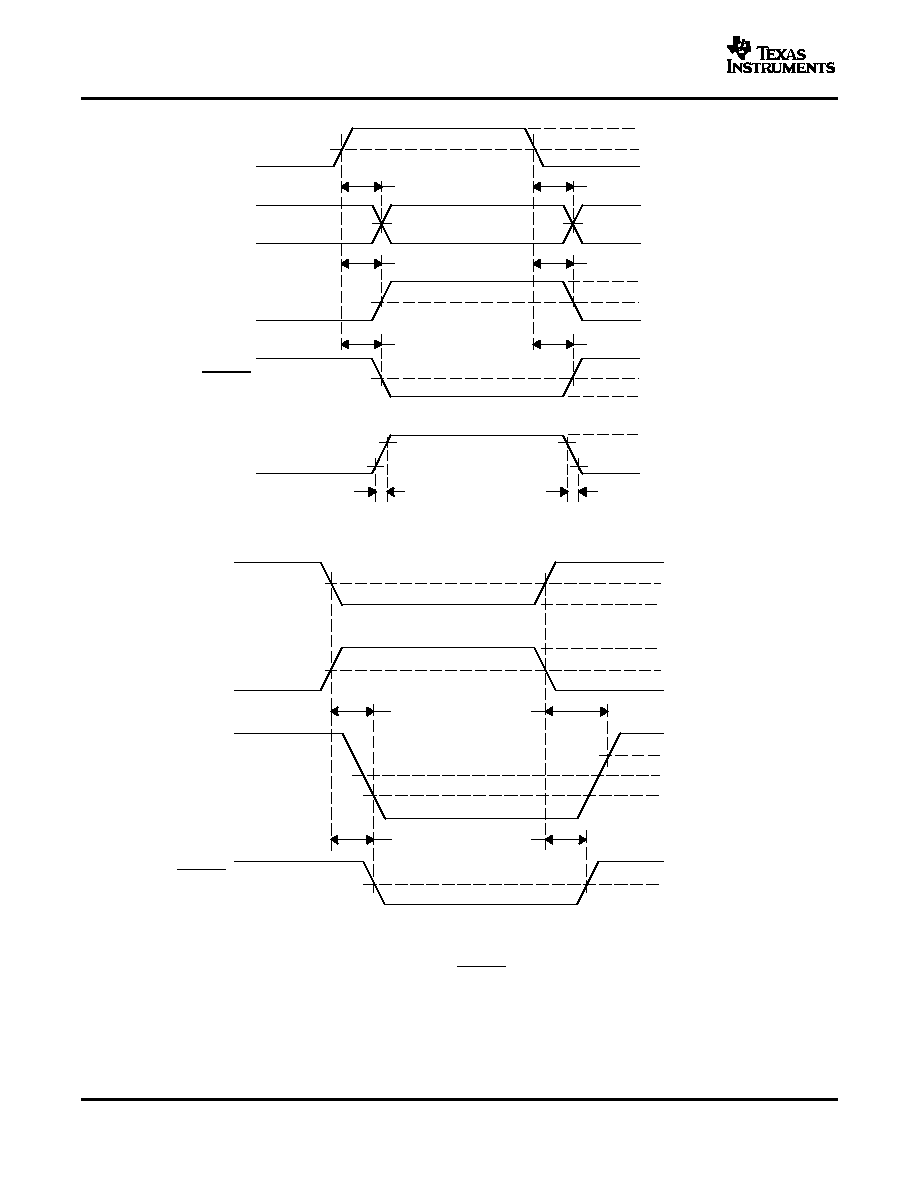
t
P1
t
PHH
t
PHL
t
P2
t
PLL
t
PLH
t
tLH
80%
20%
t
tHL
80%
20%
2.4 V
1.5 V
0.4 V
V
OH
V
OL
V
OH
(V
OH
+ V
OL
)/2
V
OL
V
OH
(V
OH
+ V
OL
)/2
V
OL
V
OH
V
OL
INPUT
OUTPUTS
OUTPUT
OUTPUT
OUTPUT
(1)
E2 = 1 while E1 changes state
(2)
E1 = 0 while E2 changes state
NOTE: In the third state, both outputs (OUTPUT and OUTPUT) are 0.1 V (max).
2.4 V
1.5 V
0.4 V
2.4 V
1.5 V
0.4 V
V
OH
V
OL
+ 0.2 V
V
OL
V
OL
- 0.1 V
V
OL
V
OL
- 0.1 V
t
PHZ
t
PZH
t
PLZ
t
PZL
E1
(1)
E2
(2)
OUTPUT
OUTPUT
TB5D1M, TB5D2H
SLLS579B ≠ SEPTEMBER 2003 ≠ REVISED MAY 2004
Figure 1. Propagation Delay Time Waveforms
Figure 2. Enable and Disable Delay Time Waveforms
6

www.ti.com
test conditions
C
L
200
200
100
C
L
OUTPUT
OUTPUT
C
L
75
75
100
C
L
OUTPUT
OUTPUT
Note: All input pulses are supplied by a generator having the following characteristics: t
r
or t
f
= 1 ns, pulse repetition rate
(PRR) = 0.25 Mbps, pulse width = 500
±
10 ns. C
P
includes the instrumentation and fixture capacitance within 0,06 m of the D.U.T.
The measurement of V
OC(PP)
is made on test equipment with a ≠3 dB bandwidth of at least 1 GHz.
C
L
200
200
50
C
L
C
P
= 2 pF
50
V
OC
V
OC(PP)
V
OH
V
OL
OUTPUT
V
OC
C
L
75
75
50
C
L
C
P
= 2 pF
50
V
OC
Note: V
OC(PP)
load circuit for 5-V nominal supplies.
Note: V
OC(PP)
load circuit for 3.3-V nominal supplies.
OUTPUT
OUTPUT
OUTPUT
OUTPUT
TB5D1M, TB5D2H
SLLS579B ≠ SEPTEMBER 2003 ≠ REVISED MAY 2004
Parametric values specified under the Electrical Characteristics and Switching Characteristics sections are
measured with the following output load circuit.
Figure 3. Driver Test Circuits, 5-V Nominal Supplies
Figure 4. Driver Test Circuits, 3.3-V Nominal Supplies
Figure 5. Test Circuits and Definitions for the Driver Common-Mode Output Voltage
7
www.ti.com
Note: Surges may be applied simultaneously, but never in opposite polarities.
Surge test pulses have t
r
= t
f
= 2
µ
s, pulse width = 7
µ
s (50% points), and
period = 250 ms.
110
110
Lightning Surge
Test Generators
_
+
_
+
V
CC
DUT
TB5D1M, TB5D2H
SLLS579B ≠ SEPTEMBER 2003 ≠ REVISED MAY 2004
Figure 6. Lightning-Surge Testing Configuration for TB5D1M
8
www.ti.com
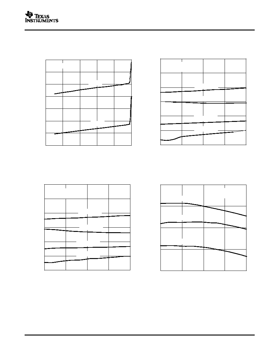
TYPICAL CHARACTERISTICS
-3
-2.5
-2
-1.5
-1
-0.5
0
-50
0
50
100
150
T
A
- Free-Air Temperature -
∞
C
V
OH
Max
V
OH
Min
V
OL
Max
V
OL
Min
V
CC
= 4.5 V to 5.5 V,
Figure 3 Load
- Output V
oltage Relative T
o
V
CC
V
O
- V
-3.5
-3
-2.5
-2
-1.5
-1
-0.5
0
-50
-40
-30
-20
-10
0
V
OH
V
OL
- Output V
oltage Relative T
o
V
CC
V
O
- V
I
O
- Output Current - mA
T
A
= 25
5
C
-3
-2.5
-2
-1.5
-1
-0.5
0
-50
0
50
100
150
T
A
- Free-Air Temperature -
∞
C
V
OH
Max
V
OH
Min
V
OL
Max
V
OL
Min
V
CC
= 3 V to 3.6 V,
Figure 4 Load
- Output V
oltage Relative T
o
V
CC
V
O
- V
0.8
1
1.2
1.4
1.6
-50
0
50
100
150
V
OD
- Differential Output V
oltage - V
T
A
- Free-Air Temperature -
∞
C
V
OD
Max
V
OD
Nom
V
OD
Min
V
CC
= 4.5 V to 5.5 V,
Figure 3 Load
TB5D1M, TB5D2H
SLLS579B ≠ SEPTEMBER 2003 ≠ REVISED MAY 2004
OUTPUT VOLTAGE RELATIVE TO V
CC
OUTPUT VOLTAGE RELATIVE TO V
CC
vs
vs
OUTPUT CURRENT
FREE-AIR TEMPERATURE
Figure 7.
Figure 8.
OUTPUT VOLTAGE RELATIVE TO V
CC
DIFFERENTIAL OUTPUT VOLTAGE
vs
vs
FREE-AIR TEMPERATURE
FREE-AIR TEMPERATURE
Figure 9.
Figure 10.
9
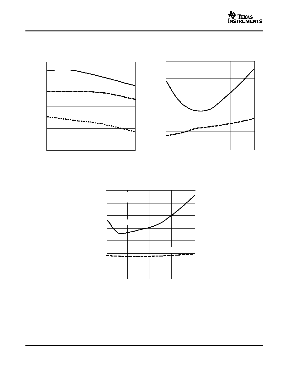
www.ti.com
0
0.8
1
1.2
1.4
1.6
-50
0
50
100
150
T
A
- Free-Air Temperature -
5
C
Max Delay
Min Delay
V
CC
= 4.5 V to 5.5 V,
Figure 3 Load
- Propagation Delay T
ime - ns
t
P
0.6
0.8
1
1.2
1.4
-50
0
50
100
150
V
OD
- Differential Output V
oltage - V
T
A
- Free-Air Temperature -
∞
C
V
OD
Max
V
OD
Nom
V
OD
Min
V
CC
= 3 V to 3.6 V,
Figure 4 Load
0
0.5
1
1.5
2
2.5
3
3.5
-50
0
50
100
150
- Propagation Delay T
ime - ns
t
P
T
A
- Free-Air Temperature -
5
C
Max Delay
V
CC
= 3 V to 3.6 V,
Figure 4 Load
Min Delay
TB5D1M, TB5D2H
SLLS579B ≠ SEPTEMBER 2003 ≠ REVISED MAY 2004
TYPICAL CHARACTERISTICS (continued)
DIFFERENTIAL OUTPUT VOLTAGE
PROPAGATION DELAY TIME t
P1
or t
P2
vs
vs
FREE-AIR TEMPERATURE
FREE-AIR TEMPERATURE
Figure 11.
Figure 12.
PROPAGATION DELAY TIME t
P1
or t
P2
vs
FREE-AIR TEMPERATURE
Figure 13.
10

www.ti.com
APPLICATION INFORMATION
Power dissipation
S
(V
Sn
I
Sn
)
(1)
S
(V
Ln
I
Ln
)
(2)
T
J
+
T
A
)
(P
D
q
JA
)
(3)
T
J
+
T
A
)
(P
D
q
JA(S)
)
(4)
q
JA(S)
+
(
q
JC
) q
CA
)
(
q
JB
) q
BA
)
(
q
JC
) q
CA
) q
JB
) q
BA
)
40
60
80
100
120
140
0
100
200
300
400
500
D, Low-K
DW, Low-K
D, High-K
DW, High-K
Thermal Impedance - C/W
Air Flow - LFM
TB5D1M, TB5D2H
SLLS579B ≠ SEPTEMBER 2003 ≠ REVISED MAY 2004
the
device
and
PCB.
JEDEC/EIA
has
defined
standardized test conditions for measuring
JA
. Two
commonly used conditions are the low-K and the
The power dissipation rating, often listed as the
high-K
boards,
covered
by
EIA/JESD51-3
and
package dissipation rating, is a function of the ambi-
EIA/JESD51-7 respectively. Figure 14 shows the
ent temperature, T
A
, and the airflow around the
low-K and high-K values of
JA
versus air flow for this
device. This rating correlates with the device's maxi-
device and its package options.
mum junction temperature, sometimes listed in the
The standardized
JA
values may not accurately
absolute maximum ratings tables. The maximum
represent the conditions under which the device is
junction temperature accounts for the processes and
used. This can be due to adjacent devices acting as
materials used to fabricate and package the device,
heat sources or heat sinks, to nonuniform airflow, or
in addition to the desired life expectancy.
to the system PCB having significantly different ther-
There are two common approaches to estimating the
mal characteristics than the standardized test PCBs.
internal die junction temperature, T
J
. In both of these
The second method of system thermal analysis is
methods, the device's internal power dissipation, P
D
,
more accurate. This calculation uses the power
needs to be calculated. This is done by totaling the
dissipation and ambient temperature, along with two
supply power(s) to arrive at the system power dissi-
device and two system-level parameters:
pation:
∑
JC
, the junction-to-case thermal resistance, in
degrees Celsius per watt
∑
JB
, the junction-to-board thermal resistance, in
and then subtracting the total power dissipation of the
degrees Celsius per watt
external load(s):
∑
CA
, the case-to-ambient thermal resistance, in
degrees Celsius per watt
∑
BA
, the board-to-ambient thermal resistance, in
The first T
J
calculation uses the power dissipation
degrees Celsius per watt.
and ambient temperature, along with one parameter:
JA
, the junction-to-ambient thermal resistance, in
In this analysis, there are two parallel paths, one
degrees Celsius per watt.
through the case (package) to the ambient, and
another through the device to the PCB to the ambi-
The product of P
D
and
JA
is the junction temperature
ent. The system-level junction-to-ambient thermal im-
rise above the ambient temperature. Therefore:
pedance,
JA(S)
, is the equivalent parallel impedance
of the two parallel paths:
where
The device parameters
JC
and
JB
account for the
internal structure of the device. The system-level
parameters
CA
and
BA
take into account details of
the PCB construction, adjacent electrical and mech-
anical components, and the environmental conditions
including airflow. Finite element (FE), finite difference
(FD), or computational fluid dynamics (CFD) pro-
grams can determine
CA
and
BA
. Details on using
these programs are beyond the scope of this data
sheet, but are available from the software manufac-
turers.
Figure 14. Thermal Impedance vs Air Flow
Note that
JA
is highly dependent on the PCB on
which the device is mounted, and on the airflow over
11
www.ti.com
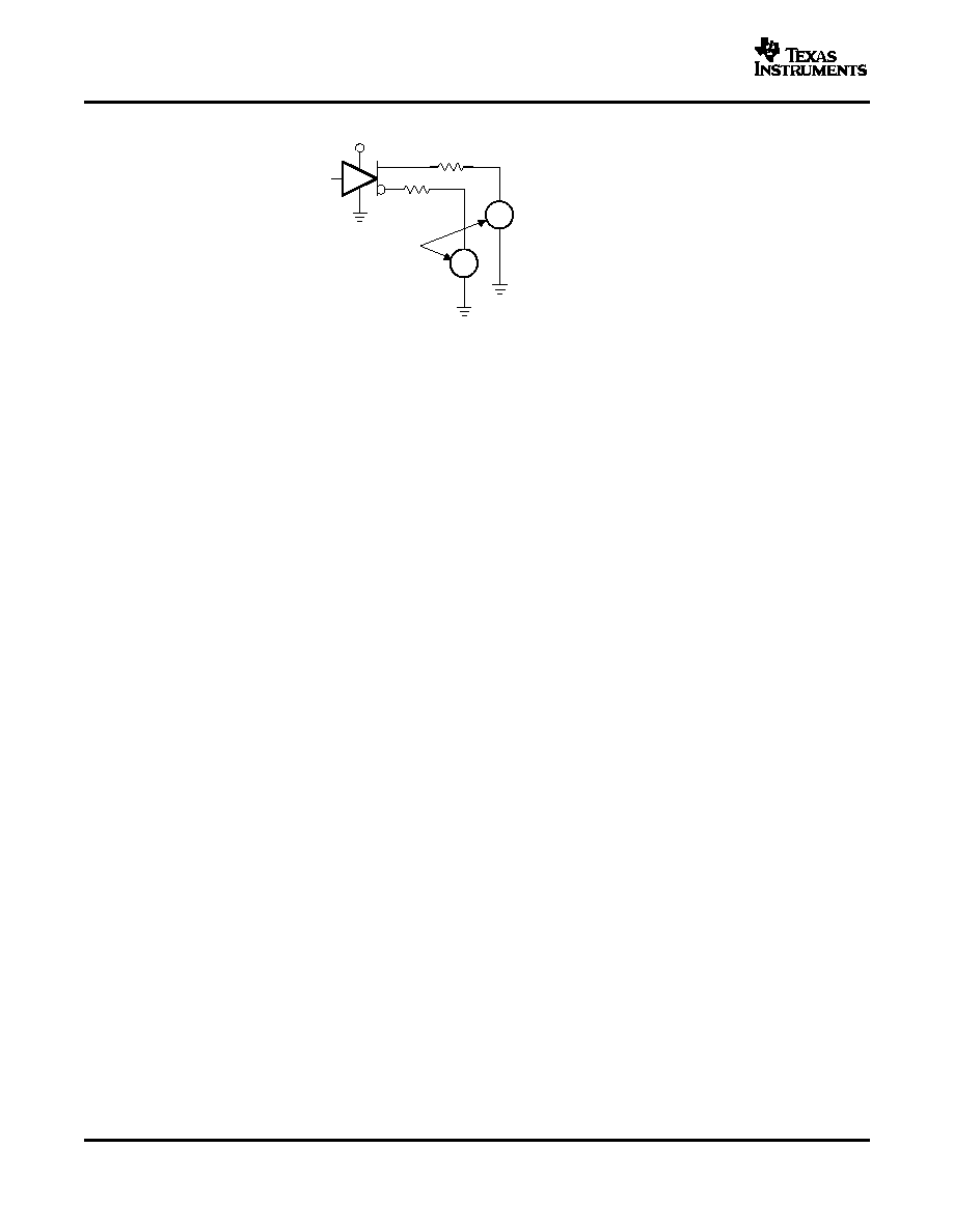
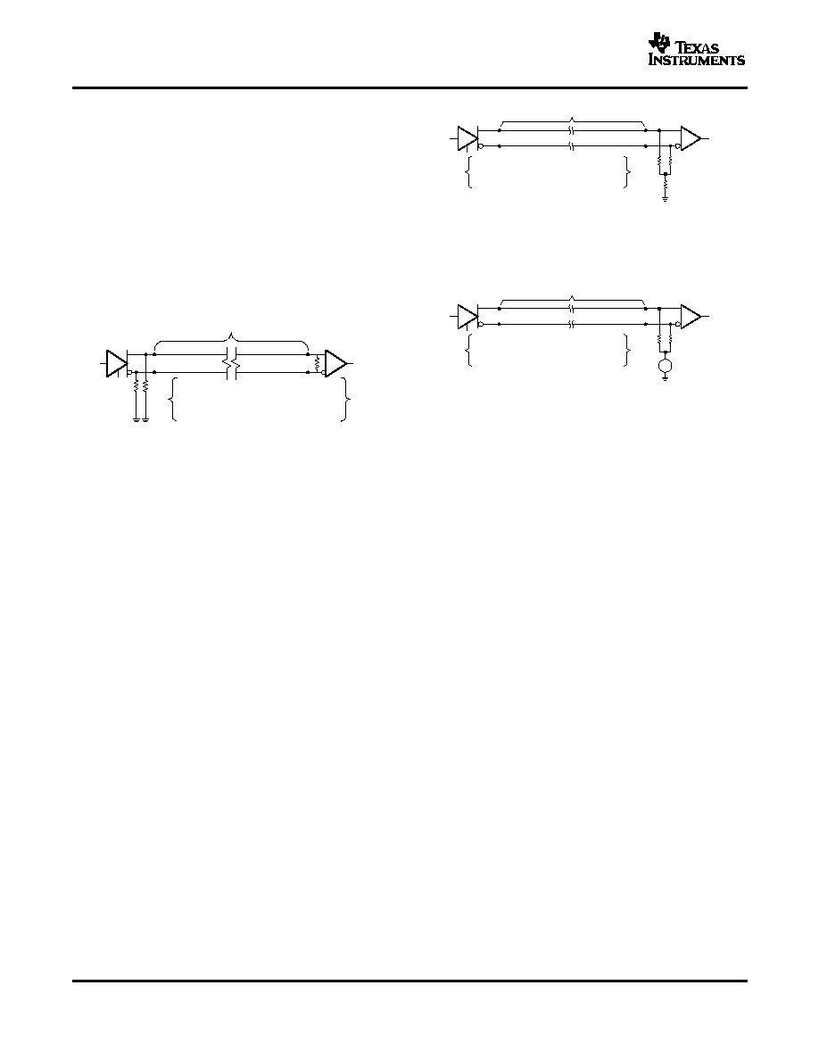
Load Circuits
Recommended Resistor Values:
For 5 V Nom Supplies, R
T
= 200
, R
S
= 90
For 3.3 V Nom Supplies, R
T
= 100
, R
S
= 30
R
T
/2
Transmission Line
OUTPUT
INPUT
R
S
R
T
/2
Recommended Resistor Values:
For 5 V and 3.3 V Nom Supplies, R
T
= 100
,
V
T
= V
CC
- 2.55 V
R
T
/2
Transmission Line
OUTPUT
INPUT
V
T
R
T
/2
_
+
INPUT
R
T
= 100
W
OUTPUT
R
S
R
S
Transmission Line
Recommended Resistor Values:
For 5-V Nominal Supplies, R
S
= 200
W
For 3.3-V Nominal Supplies, R
S
= 75
W
TB5D1M, TB5D2H
SLLS579B ≠ SEPTEMBER 2003 ≠ REVISED MAY 2004
The test load circuits shown in Figure 3 and Figure 4
are based on a recommended pi type of load circuit
shown in Figure 15. The 100-
differential load
resistor R
T
at the receiver provide proper termination
for the interconnecting transmission line, assuming it
has a 100-
characteristic impedance. The two
resistors R
S
to ground at the driver end of the
Figure 16. A Recommended Y Load Circuit
transmission line link provide dc current paths for the
emitter follower output transistors. The two resistors
An additional load circuit, similar to one commonly
to ground normally should not be placed at the
used with ECL and PECL, is shown in Figure 17.
receiver end, as they shunt the termination resistor,
potentially creating an impedance mismatch with
undesirable reflections.
Figure 17. A Recommended PECL-Style Load
Circuit
Figure 15. A Recommended pi Load Circuit
An important feature of all of these recommended
load circuits is that they ensure that both of the
Another common load circuit, a Y load, is shown in
emitter follower output transistors remain active
Figure 16. The receiver-end line termination of R
T
is
(conducting current) at all times. When deviating from
provided by the series combination of the two RT/2
these recommended values, it is important to make
resistors, while the dc current path to ground is
sure that the low-side output transistor does not turn
provided by the single resistor R
S
. Recommended
off. Failure to do so increases the t
skew2
and V
OC(PP)
values, as a function of the nominal supply voltage
values, increasing the potential for electromagnetic
range, are indicated in the figure.
radiation.
12

PACKAGING INFORMATION
Orderable Device
Status
(1)
Package
Type
Package
Drawing
Pins Package
Qty
Eco Plan
(2)
Lead/Ball Finish
MSL Peak Temp
(3)
TB5D1MD
ACTIVE
SOIC
D
16
40
Pb-Free
(RoHS)
CU NIPDAU
Level-2-250C-1YEAR/
Level-1-220C-UNLIM
TB5D1MDR
ACTIVE
SOIC
D
16
2500
Pb-Free
(RoHS)
CU NIPDAU
Level-2-250C-1YEAR/
Level-1-220C-UNLIM
TB5D1MDW
ACTIVE
SOIC
DW
16
40
Pb-Free
(RoHS)
CU NIPDAU
Level-2-250C-1YEAR/
Level-1-220C-UNLIM
TB5D1MDWR
ACTIVE
SOIC
DW
16
2000
Pb-Free
(RoHS)
CU NIPDAU
Level-2-250C-1YEAR/
Level-1-220C-UNLIM
TB5D2HD
ACTIVE
SOIC
D
16
40
Pb-Free
(RoHS)
CU NIPDAU
Level-2-250C-1YEAR/
Level-1-220C-UNLIM
TB5D2HDR
ACTIVE
SOIC
D
16
2500
Pb-Free
(RoHS)
CU NIPDAU
Level-2-250C-1YEAR/
Level-1-220C-UNLIM
TB5D2HDW
ACTIVE
SOIC
DW
16
40
Pb-Free
(RoHS)
CU NIPDAU
Level-2-250C-1YEAR/
Level-1-220C-UNLIM
TB5D2HDWR
ACTIVE
SOIC
DW
16
2000
Pb-Free
(RoHS)
CU NIPDAU
Level-2-250C-1YEAR/
Level-1-220C-UNLIM
(1)
The marketing status values are defined as follows:
ACTIVE: Product device recommended for new designs.
LIFEBUY: TI has announced that the device will be discontinued, and a lifetime-buy period is in effect.
NRND: Not recommended for new designs. Device is in production to support existing customers, but TI does not recommend using this part in
a new design.
PREVIEW: Device has been announced but is not in production. Samples may or may not be available.
OBSOLETE: TI has discontinued the production of the device.
(2)
Eco Plan - May not be currently available - please check
http://www.ti.com/productcontent
for the latest availability information and additional
product content details.
None: Not yet available Lead (Pb-Free).
Pb-Free (RoHS): TI's terms "Lead-Free" or "Pb-Free" mean semiconductor products that are compatible with the current RoHS requirements
for all 6 substances, including the requirement that lead not exceed 0.1% by weight in homogeneous materials. Where designed to be soldered
at high temperatures, TI Pb-Free products are suitable for use in specified lead-free processes.
Green (RoHS & no Sb/Br): TI defines "Green" to mean "Pb-Free" and in addition, uses package materials that do not contain halogens,
including bromine (Br) or antimony (Sb) above 0.1% of total product weight.
(3)
MSL, Peak Temp. -- The Moisture Sensitivity Level rating according to the JEDECindustry standard classifications, and peak solder
temperature.
Important Information and Disclaimer:The information provided on this page represents TI's knowledge and belief as of the date that it is
provided. TI bases its knowledge and belief on information provided by third parties, and makes no representation or warranty as to the
accuracy of such information. Efforts are underway to better integrate information from third parties. TI has taken and continues to take
reasonable steps to provide representative and accurate information but may not have conducted destructive testing or chemical analysis on
incoming materials and chemicals. TI and TI suppliers consider certain information to be proprietary, and thus CAS numbers and other limited
information may not be available for release.
In no event shall TI's liability arising out of such information exceed the total purchase price of the TI part(s) at issue in this document sold by TI
to Customer on an annual basis.
PACKAGE OPTION ADDENDUM
www.ti.com
4-Feb-2005
Addendum-Page 1


IMPORTANT NOTICE
Texas Instruments Incorporated and its subsidiaries (TI) reserve the right to make corrections, modifications,
enhancements, improvements, and other changes to its products and services at any time and to discontinue
any product or service without notice. Customers should obtain the latest relevant information before placing
orders and should verify that such information is current and complete. All products are sold subject to TI's terms
and conditions of sale supplied at the time of order acknowledgment.
TI warrants performance of its hardware products to the specifications applicable at the time of sale in
accordance with TI's standard warranty. Testing and other quality control techniques are used to the extent TI
deems necessary to support this warranty. Except where mandated by government requirements, testing of all
parameters of each product is not necessarily performed.
TI assumes no liability for applications assistance or customer product design. Customers are responsible for
their products and applications using TI components. To minimize the risks associated with customer products
and applications, customers should provide adequate design and operating safeguards.
TI does not warrant or represent that any license, either express or implied, is granted under any TI patent right,
copyright, mask work right, or other TI intellectual property right relating to any combination, machine, or process
in which TI products or services are used. Information published by TI regarding third-party products or services
does not constitute a license from TI to use such products or services or a warranty or endorsement thereof.
Use of such information may require a license from a third party under the patents or other intellectual property
of the third party, or a license from TI under the patents or other intellectual property of TI.
Reproduction of information in TI data books or data sheets is permissible only if reproduction is without
alteration and is accompanied by all associated warranties, conditions, limitations, and notices. Reproduction
of this information with alteration is an unfair and deceptive business practice. TI is not responsible or liable for
such altered documentation.
Resale of TI products or services with statements different from or beyond the parameters stated by TI for that
product or service voids all express and any implied warranties for the associated TI product or service and
is an unfair and deceptive business practice. TI is not responsible or liable for any such statements.
Following are URLs where you can obtain information on other Texas Instruments products and application
solutions:
Products
Applications
Amplifiers
amplifier.ti.com
Audio
www.ti.com/audio
Data Converters
dataconverter.ti.com
Automotive
www.ti.com/automotive
DSP
dsp.ti.com
Broadband
www.ti.com/broadband
Interface
interface.ti.com
Digital Control
www.ti.com/digitalcontrol
Logic
logic.ti.com
Military
www.ti.com/military
Power Mgmt
power.ti.com
Optical Networking
www.ti.com/opticalnetwork
Microcontrollers
microcontroller.ti.com
Security
www.ti.com/security
Telephony
www.ti.com/telephony
Video & Imaging
www.ti.com/video
Wireless
www.ti.com/wireless
Mailing Address:
Texas Instruments
Post Office Box 655303 Dallas, Texas 75265
Copyright
2005, Texas Instruments Incorporated