 | ÐлекÑÑоннÑй компоненÑ: TC217 | СкаÑаÑÑ:  PDF PDF  ZIP ZIP |
Äîêóìåíòàöèÿ è îïèñàíèÿ www.docs.chipfind.ru
TC217
1158-
×
488-PIXEL CCD IMAGE SENSOR
SOCS015C OCTOBER 1989 REVISED JUNE 1996
Copyright
©
1996, Texas Instruments Incorporated
1
POST OFFICE BOX 655303
·
DALLAS, TEXAS 75265
·
High-Resolution, Solid-State Monochrome
Image Sensor for Video or Still-Picture
Photography
·
Frame Transfer With Two Field Memories
Allows Multimode Operation
·
1134 (H) x 486 (V) Active Elements in
Image-Sensing Area
·
11-mm Image-Area Diagonal is Compatible
With 2/3" Vidicon Optics
·
Fast Clear Capability
·
Electron-Hole Recombination Antiblooming
·
Dynamic Range . . . More Than 60 dB
·
High Photoresponse Uniformity
·
On-Chip Cross-Coupled Resets for Easy
Off-Chip Implementation of CCSH Video
Signal Processing
·
Solid-State Reliability With No Image
Burn-in, Residual Imaging, Image
Distortion, Image Lag, or Microphonics
description
The TC217 is a frame-transfer charge-coupled-device (CCD) image sensor with two field memories. It is
suitable for use in NTSC video or still-picture photography applications. Its image-sensing area is configured
into 488 lines; 486 of these are active and the remaining two are used for dark reference. Each line is configured
into 1158 pixels with 1134 active and 24 for dark reference. The TC217 has a standard aspect ratio of 4:3 and
a standard 11-mm image-sensing-area diagonal. Its blooming protection, which is an integral part of each pixel,
is based on electron-hole recombination and is activated by clocking the antiblooming gate.
One important aspect of the TC217 high-resolution sensor is its ability to simultaneously capture both fields of
a TV frame. Its two independently addressable memories allow separate storage of each field and operation
in a variety of modes, including EIA-170 (formerly RS-170) with true interlace, EIA-170 with pseudointerlace,
and nonstandard pseudointerlace with a resolution of 972 lines.
A unique multiplexer section (see Figure 3) rearranges the horizontal pixels into vertical groups of three and
separates and loads the image into the two field memories. The independent addressing of each field memory
provides flexibility for different modes of operation. The interdigitated layout of the memories allows each
memory to share the same bank of three serial registers and associated charge detection amplifiers (see
Figure 4 and the functional block diagram). Each register and associated amplifier reads out every third column
of the image area (see Figure 5). The three amplifiers are optimized dual source-followers that allow the use
of off-chip double-correlated clamp-sample-and-hold amplifiers for removing KTC noise.
The TC217 is built using TI-proprietary virtual-phase technology, which provides devices with high blue
response, low dark signal, good uniformity, and single-phase clocking. The TC217 is characterized for operation
from 10
°
C to 40
°
C.
This MOS device contains limited built-in gate protection. During storage or handling, the device leads should be shorted together
or the device should be placed in conductive foam. In a circuit, unused inputs should always be connected to SUB. Under no
circumstances should pin voltages exceed absolute maximum ratings. Avoid shorting OUTn to ADB during operation to prevent
damage to the amplifier. The device can also be damaged if the output terminals are reverse-biased and an excessive current is
allowed to flow. Specific guidelines for handling devices of this type are contained in the publication
Guidelines for Handling
Electrostatic-Discharge-Sensitive (ESDS) Devices and Assemblies available from Texas Instruments.
SUB
CDB
AMP GND
OUT1
OUT2
OUT3
ADB
SAG1
IAG
ABG
SUB
SUB
TRG
SRG1
SRG2
SRG3
SAG2
TMG
IAG
ABG
TDB
SUB
22
21
20
19
18
17
16
15
14
13
12
11
10
9
8
7
6
5
4
3
2
1
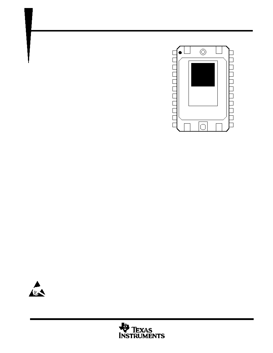
DUAL-IN-LINE PACKAGE
(TOP VIEW)
PRODUCTION DATA information is current as of publication date.
Products conform to specifications per the terms of Texas Instruments
standard warranty. Production processing does not necessarily include
testing of all parameters.
TC217
1158-
×
488-PIXEL CCD IMAGE SENSOR
SOCS015C OCTOBER 1989 REVISED JUNE 1996
2
POST OFFICE BOX 655303
·
DALLAS, TEXAS 75265
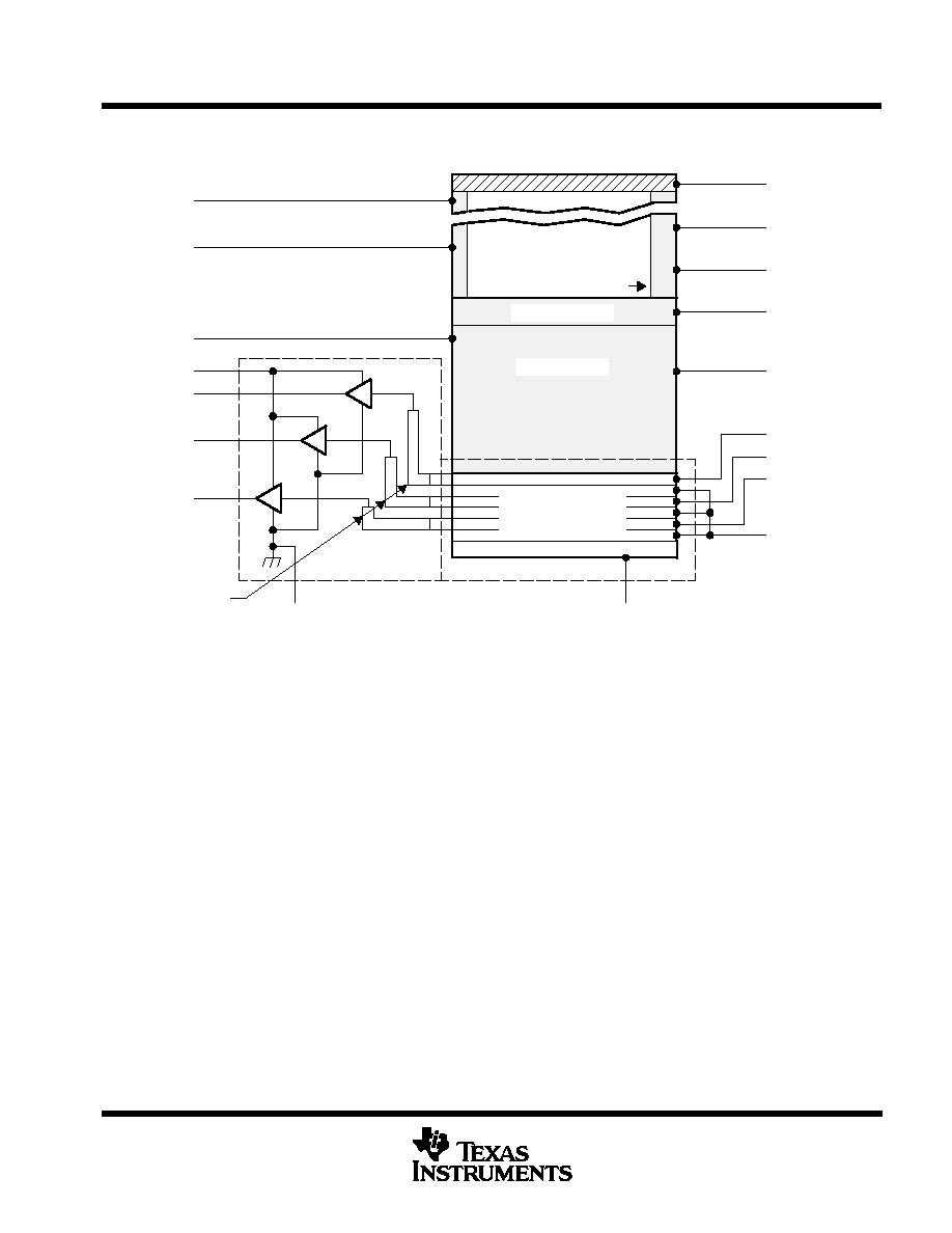
functional block diagram
Clearing Drain
Dark Reference Elements
Amplifiers
OUT2
OUT3
ADB
ABG
SAG1
IAG
3
4
2
5
6
7
8
OUT1
9
AMP GND
SRG3
SRG2
SRG1
TRG
CDB
10
13
14
15
16
SAG2
17
IAG
TBD
19
21
ÎÎÎÎÎÎÎÎÎÎÎ
ÎÎÎÎÎÎÎÎÎÎÎ
Storage Area
Blooming Protection
Image Area With
Top Drain
12 Dummy
Elements
ABG
20
TMG
18
3:2 Multiplexer
Transfer Gates
and
Serial Registers
TC217
1158-
×
488-PIXEL CCD IMAGE SENSOR
SOCS015C OCTOBER 1989 REVISED JUNE 1996
3
POST OFFICE BOX 655303
·
DALLAS, TEXAS 75265
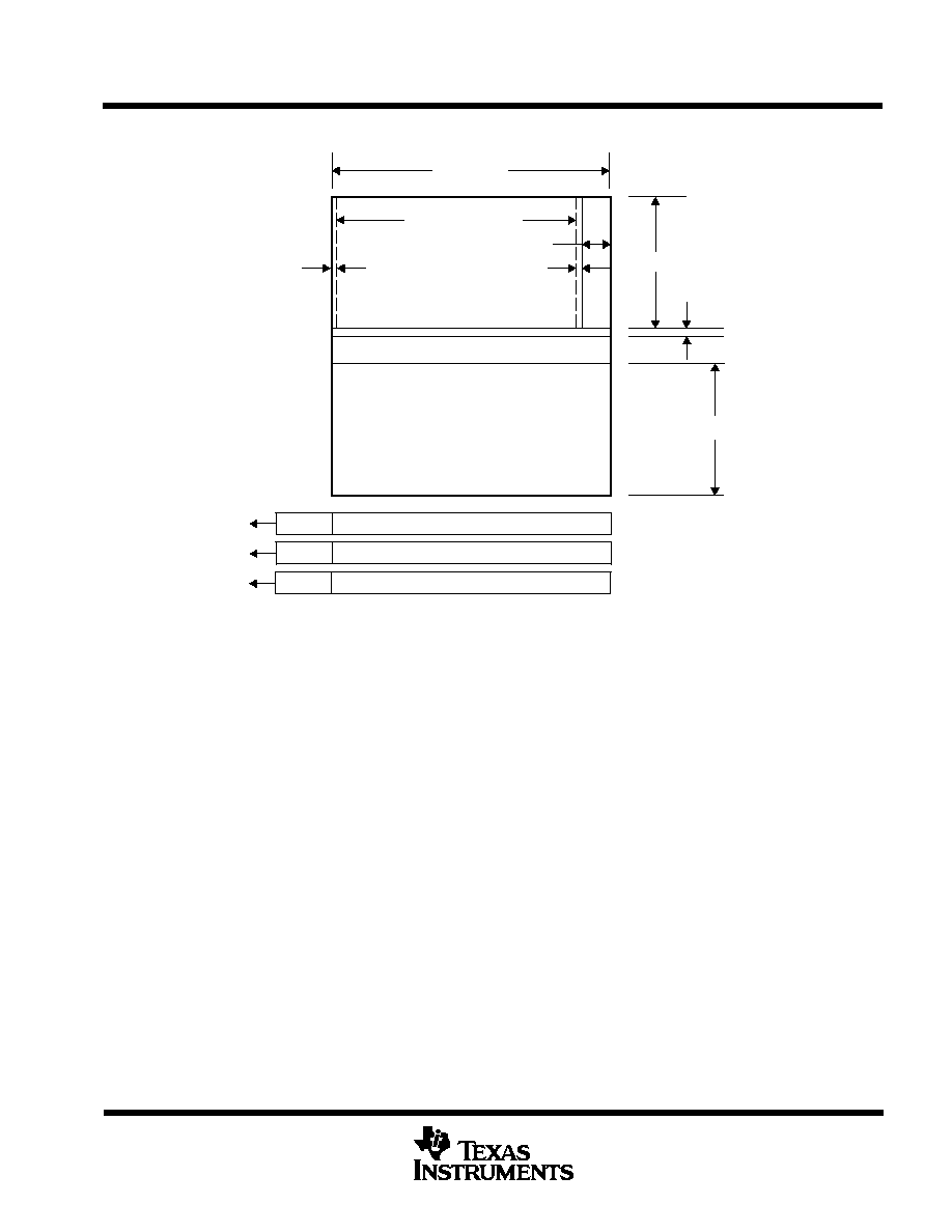
sensor topology diagram
ÉÉÉÉÉÉÉÉÉÉÉÉÉ
ÉÉÉÉÉÉÉÉÉÉÉÉÉ
ÉÉ
ÉÉ
ÉÉ
ÉÉ
ÉÉ
ÉÉ
ÉÉ
ÉÉ
ÉÉ
ÉÉ
ÉÉ
ÉÉ
1/2 Dark Pixel
2 Dark Lines
12
Dummy Pixels
486 Active Lines
386
12
386
732 Lines
12
386
1/2 Dark Pixel
23 Dark Pixels
Multiplexer
1158 Pixels
1134 Active Pixels
TC217
1158-
×
488-PIXEL CCD IMAGE SENSOR
SOCS015C OCTOBER 1989 REVISED JUNE 1996
4
POST OFFICE BOX 655303
·
DALLAS, TEXAS 75265
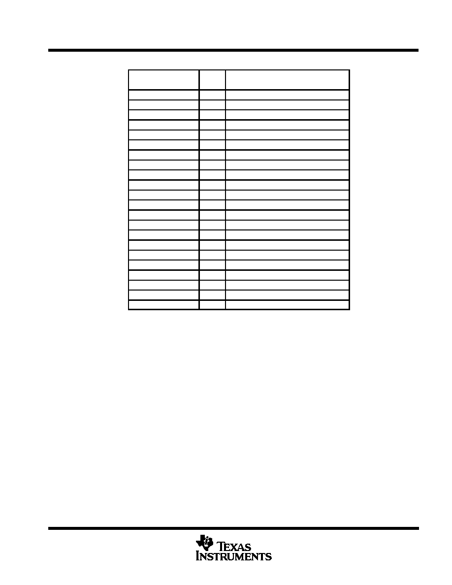
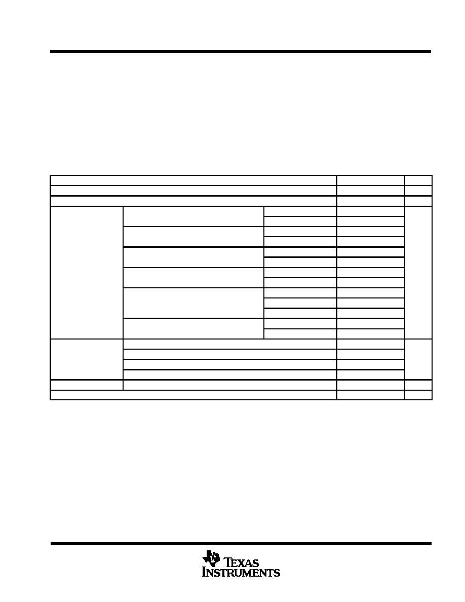
Terminal Functions
TERMINAL
I/O
DESCRIPTION
NAME
NO.
I/O
DESCRIPTION
ABG
2
I
Antiblooming gate
ABG
20
I
Antiblooming gate
ADB
5
I
Supply voltage for amplifier drain bias
AMP GND
9
Amplifier ground
CDB
10
I
Supply voltage for clearing drain bias
IAG
3
I
Image-area gate
IAG
19
I
Image-area gate
OUT1
8
O
Output signal 1
OUT2
7
O
Output signal 2
OUT3
6
O
Output signal 3
SAG1
4
I
Storage-area gate
SAG2
17
I
Storage-area gate
SRG1
14
I
Serial-register gate 1
SRG2
15
I
Serial-register gate 2
SRG3
16
I
Serial-register gate 3
SUB
1
Substrate and clock return
SUB
11
Substrate and clock return
SUB
12
Substrate and clock return
SUB
22
Substrate and clock return
TDB
21
I
Supply voltage for top drain bias
TMG
18
I
Transfer-multiplex gate
TRG
13
I
Transfer gate
All pins of the same name should be connected together externally (i.e., pin 2 to pin 20,
pin 3 to pin 19, etc.).
detailed description
The TC217 consists of five basic functional blocks: (1) the image-sensing area, (2) the multiplexer block, (3)
the image-storage area with dual field memories, (4) the serial register and transfer gates, and (5) the low-noise
signal-processing amplifier block with charge-detection nodes. The location of each of these blocks is identified
in the functional block diagram.
image-sensing area
Figure 1 and Figure 2 show cross sections with potential well diagrams and top views of image-sensing
elements. As light enters the silicon in the image-sensing area, free electrons are generated and collected in
the potential wells of the sensing elements. During this time, blooming protection is activated by applying a burst
of pulses to the antiblooming gate inputs every horizontal blanking interval. This prevents blooming caused by
the spilling of charge from overexposed elements into neighboring elements. There are 23 full columns and one
half-column of elements at the right edge of the image-sensing area that are shielded from incident light; these
elements provide the dark reference used in subsequent video processing circuits to restore the video black
level. There are also one half-column of light-shielded elements at the left edge of the image-sensing area and
two lines of light-shielded elements at the bottom of the image area immediately above the multiplexer (the latter
prevent charge leakage from the image area into the multiplexer).
TC217
1158-
×
488-PIXEL CCD IMAGE SENSOR
SOCS015C OCTOBER 1989 REVISED JUNE 1996
5
POST OFFICE BOX 655303
·
DALLAS, TEXAS 75265
multiplexer and storage area
After integration, the multiplexer rearranges two horizontal lines into vertical groups of three and separates and
loads the image into the storage area. Figure 3 shows the layout of the multiplexer gate and its interface to the
two field memories. Figure 4 shows the interface region between the storage area and the three serial registers.
A drain is also provided to clear the image-sensing and image-storage areas of unwanted charge. Such charge
can accumulate in the imager during the startup of operation or under special circumstances when nonstandard
TV operation is desired. The sensor's independently addressable memories allow several different modes of
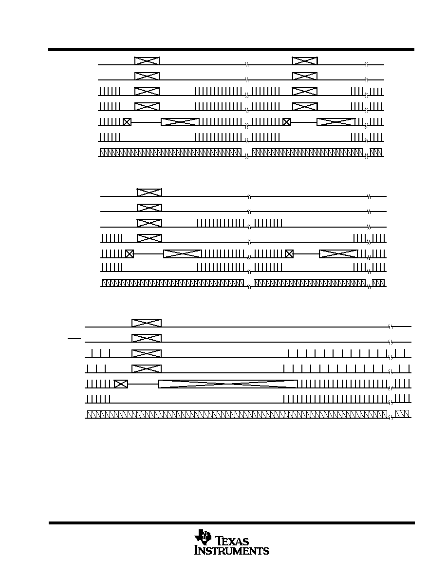
sensor operation including (1) a normal-light mode, (2) a low-light mode, and (3) a still mode. The timing for these
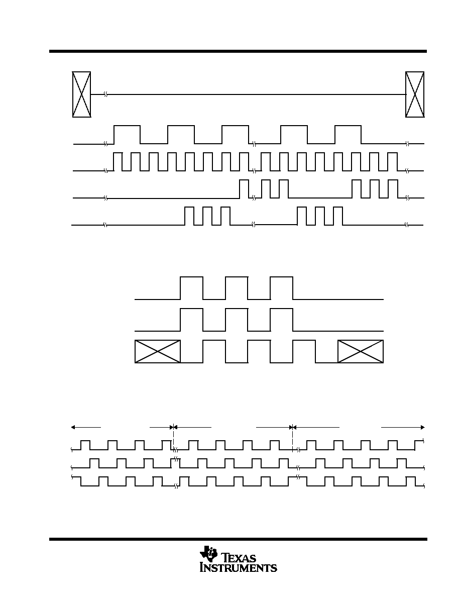
three modes is given in Figures 6, 7, and 8. The parallel-transfer timing is shown in Figure 9.
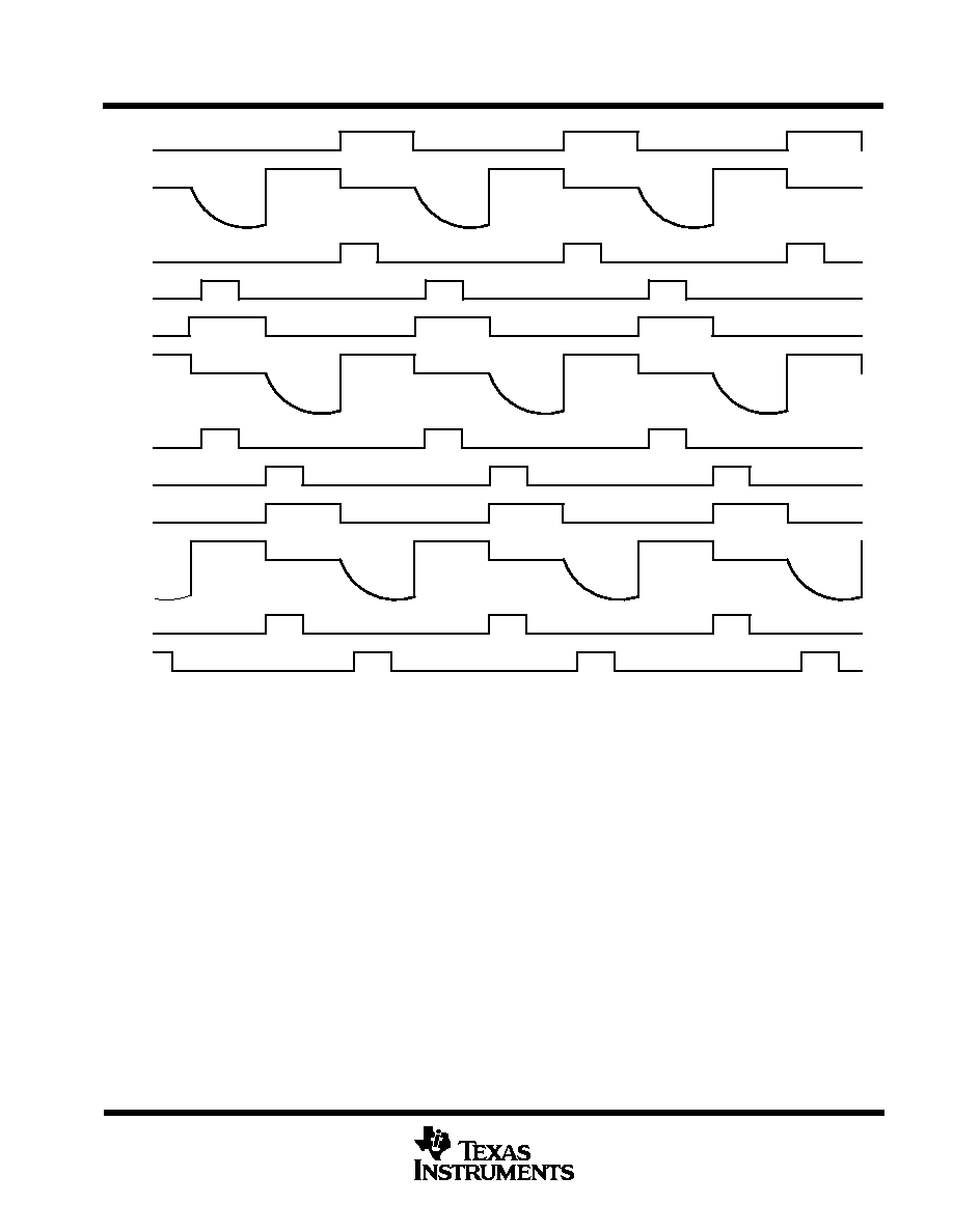
serial registers and amplifiers
After transfer to the serial registers (see Figure 10, which shows the horizontal timing that gives the necessary
sequence of pulses for transfer from the storage area to the serial registers), the charge is converted to a signal
voltage at the sense node and buffered with a dual-stage source follower. The three serial registers are typically
clocked 120 degrees out of phase with each serial-gate pulse supplying a detection node reset signal for one
of the other two serial gates. The readout timing, which includes the three serial pulses and the pixel clamp
pulses used in an off-chip double-correlated sampling circuit, is shown in Figure 12. The detection nodes and
amplifiers are located some distance away from the edge of the storage area. Therefore, 12 dummy elements
are incorporated at the end of each serial register to span the distance. The location of the dummy elements,
which are considered to be part of the amplifiers, is shown in the functional block diagram. A schematic of the
detection node and amplifier is given in Figure 5.
-ABG
-IAG
7.8
µ
m(H)
Clocked Barrier
Virtual Barrier
Antiblooming Gate
Virtual Well
Clocked Well
Light
Antiblooming
Clocking Levels
Accumulated Charge
13.6
µ
m(V)
Figure 1. Charge-Accumulation Process
-PS
Channel Stops
Virtual Phase
Clocked Phase
Figure 2. Charge-Transfer Process
TC217
1158-
×
488-PIXEL CCD IMAGE SENSOR
SOCS015C OCTOBER 1989 REVISED JUNE 1996
6
POST OFFICE BOX 655303
·
DALLAS, TEXAS 75265
Clocked Gate
Antiblooming Gate
5.8
µ
m
Channel Stops
Multiplexer
Clocked Gate
Clocked Wells
Virtual Wells
Clocked
Gate
Memory A
Clocked Gate
Memory B
Metal Bus Lines
for Memory A and B
4.5
µ
m
9
µ
m
Memory
Area
732 Lines
Multiplexer
13.6
µ
m
Image
Area
488 Lines
7.8
µ
m
11.7
µ
m
Figure 3. Layout of Multiplexing Gate
TC217
1158-
×
488-PIXEL CCD IMAGE SENSOR
SOCS015C OCTOBER 1989 REVISED JUNE 1996
7
POST OFFICE BOX 655303
·
DALLAS, TEXAS 75265
Contact Holes
to Metal Bus Lines
Clocked Gates
Memory A, B
Channel Stop
Channel Stop
Common
Virtual Well
Clocked Gate
Serial Register 1
Transfer Gate
Clocked Gate
Serial Register 2
Horizontal
Register 2
Horizontal
Register 1
Memory
Area
732 Lines
Figure 4. Layout of the Interface Region Between the Memories and the Serial Registers
TC217
1158-
×
488-PIXEL CCD IMAGE SENSOR
SOCS015C OCTOBER 1989 REVISED JUNE 1996
8
POST OFFICE BOX 655303
·
DALLAS, TEXAS 75265
VO3
VO2
VO1
VREF
ADB
Q9
Q8
Q7
Q6
Q5
Q4
Q3
Q2
Q1
SRG3
SRG2
SRG1
q
q
q
Figure 5. Circuit Diagram - Charge-Detection Amplifiers
IAG
SAG1
ABG
SAG2
TRG
SRG1, SRG2,
TMG
SRG3
Figure 6. Vertical Timing, Normal-Light Mode
TC217
1158-
×
488-PIXEL CCD IMAGE SENSOR
SOCS015C OCTOBER 1989 REVISED JUNE 1996
9
POST OFFICE BOX 655303
·
DALLAS, TEXAS 75265
IAG
SAG1
ABG
SAG2
TRG
SRG1, SRG2,
TMG
SRG3
Figure 7. Vertical Timing, Low-Light Mode
IAG
SAG1
ABG
SAG2
TRG
SRG1, SRG2,
TMG
SRG3
Figure 8. Vertical Timing, Still Mode
IAG
SAG1
ABG
SAG2
TRG
SRG1, SRG2,
TMG
SRG3
Figure 9. Vertical Timing, Progressive-Scan Mode
TC217
1158-
×
488-PIXEL CCD IMAGE SENSOR
SOCS015C OCTOBER 1989 REVISED JUNE 1996
10
POST OFFICE BOX 655303
·
DALLAS, TEXAS 75265
ABG
IAG
TMG
SAG1
SAG2
Figure 10. Parallel-Transfer Timing
SRG1, SRG2, SRG3
SAG1, SAG2
TRG
These clocks are mode-dependent.
Figure 11. Horizontal Timing
SRG1
SRG2
SRG3
Dummy Pixels
9
10
11
12
375
376
377
378
5
6
7
8
Image Pixels
Dark Pixels
Figure 12. Start of Serial-Transfer Timing
TC217
1158-
×
488-PIXEL CCD IMAGE SENSOR
SOCS015C OCTOBER 1989 REVISED JUNE 1996
11
POST OFFICE BOX 655303
·
DALLAS, TEXAS 75265
SRG1
OUT1
CL1
SH1
SRG2
OUT2
CL2
SH2
SRG3
CL3
SH3
NOTES: A. The video-processing (off-chip) pulses are defined as follows:
CL1 = Clamp pulse for video from OUT1
SH1 = Sample pulse for the sample-and-hold amplifier for video 1
CL2 = Clamp pulse for video from OUT2
SH2 = Sample pulse for the sample-and-hold amplifier for video 2
CL3 = Clamp pulse for video from OUT3
SH3 = Sample pulse for the sample-and-hold amplifier for video 3
B. The signals for channel (n +1) are phase shifted 120
°
from the signals for channel (n). For example, SRG2 is phase shifted
120
°
relative to SRG1, SRG3 is phase-shifted 120
°
relative to SRG2, OUT2 is phase shifted 120
°
relative to OUT1, OUT3 is
phase shifted 120
°
relative to OUT2, and so forth.
OUT3
Figure 13. Video-Process Timing
COLUMN AMPLITUDE, x (mV)
TC217
1158-
×
488-PIXEL CCD IMAGE SENSOR
SOCS015C OCTOBER 1989 REVISED JUNE 1996
12
POST OFFICE BOX 655303
·
DALLAS, TEXAS 75265
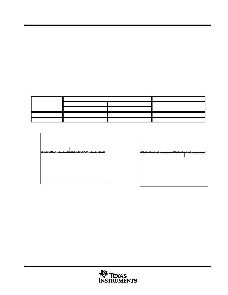
spurious nonuniformity specification
The spurious nonuniformity specification of the TC217 CCD grades 30 and 40 is based on several sensor
characteristics:
·
Amplitude of the nonuniform line or pixel
·
Polarity of the nonuniform pixel
Black
White
·
Column amplitude
The CCD sensors are characterized in both an illuminated condition and a dark condition. In the dark condition,
the nonuniformity is specified in terms of absolute amplitude as shown in Figure 14. In the illuminated condition,
the nonuniformity is specified as a percentage of the total illumination as shown in Figure 15.
The nonuniformity specification for the TC217 is as follows (CCD video-output signal is 50 mV
±
10 mV):
PIXEL NONUNIFORMITY
COLUMN NONUNIFORMITY
PART NUMBER
DARK CONDITION
ILLUMINATED CONDITION
PIXEL AMPLITUDE, x (mV)
% OF TOTAL ILLUMINATION
TC217-30
x
12 mV
x
10
x < 0.5 mV
TC217-40
x
15 mV
x
15
x
1 mV
mV
Amplitude
t
Illumination
% of Total
t
Figure 14. Pixel Nonuniformity,
Figure 15. Pixel Nonuniformity,
Dark Condition
Illuminated Condition
TC217
1158-
×
488-PIXEL CCD IMAGE SENSOR
SOCS015C OCTOBER 1989 REVISED JUNE 1996
13
POST OFFICE BOX 655303
·
DALLAS, TEXAS 75265
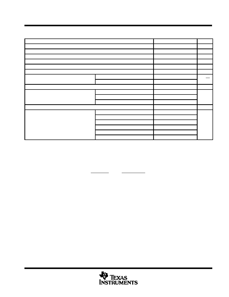
absolute maximum ratings over operating free-air temperature range (unless otherwise noted)
Supply voltage range for ADB, CDB, TDB (see Note 1)
0 V to 15 V
. . . . . . . . . . . . . . . . . . . . . . . . . . . . . . . . . . .
Input voltage range for ABG, IAG, SAG1, SAG2, SRG1, SRG2, SRG3, TRG
15 V to 15 V
. . . . . . . . . . . . .
Operating free-air temperature range
30
°
C to 85
°
C
. . . . . . . . . . . . . . . . . . . . . . . . . . . . . . . . . . . . . . . . . . . . . . . .
Storage temperature range, T
A
30
°
C to 85
°
C
. . . . . . . . . . . . . . . . . . . . . . . . . . . . . . . . . . . . . . . . . . . . . . . . . . . . .
Lead temperature 1,6 mm (1/16 inch) from case for 10 seconds
260
°
C
. . . . . . . . . . . . . . . . . . . . . . . . . . . . . . .
Stresses beyond those listed under "absolute maximum ratings" may cause permanent damage to the device. These are stress ratings only, and
functional operation of the device at these or any other conditions beyond those indicated under "recommended operating conditions" is not
implied. Exposure to absolute-maximum-rated conditions for extended periods may affect device reliability.
NOTE 1: All voltage values are with respect to the substrate terminal.
recommended operating conditions
MIN
NOM
MAX
UNIT
Supply voltage for ADB, CDB, TDB
11
12
13
V
Substrate bias voltage
0
V
IAG
High level
2
2.5
3
IAG
Low level
11
9
SAG1 SAG2
High level
2
2.5
3
SAG1, SAG2
Low level
11
9
SRG1 SRG2 SRG3
High level
2
2.5
3
SRG1, SRG2, SRG3
Low level
11
9
Input voltage, VI
TMG
High level
2
2.5
3
V
TMG
Low level
11
9
High level
4
4.5
5
ABG
Intermediate level§
2.85
2
1.55
Low level
7.5
7
6.5
TRG
High level
2
2.5
3
TRG
Low level
11
9
ABG
1
Clock frequency f l k
IAG
1.2
MHz
Clock frequency, fclock
SRG1, SRG2, SRG3, TRG
7.2
MHz
TMG, SAG1, SAG2
3.6
Capacitive load
OUT1, OUT2, OUT3
8
pF
Operating free-air temperature, TA
10
40
°
C
The algebraic convention, in which the least-positive (most negative) value is designated minimum, is used in this data sheet for clock voltage
levels.
§ Adjustment is required for optimal performance.
TC217
1158-
×
488-PIXEL CCD IMAGE SENSOR
SOCS015C OCTOBER 1989 REVISED JUNE 1996
14
POST OFFICE BOX 655303
·
DALLAS, TEXAS 75265
electrical characteristics over recommended operating ranges of supply voltage and free-air
temperature
PARAMETER
MIN
TYP
MAX
UNIT
Dynamic range (see Note 2)
60
73
dB
Charge conversion factor
6
µ
V/e
Charge transfer efficiency (see Note 3)
0.9999
0.99995
Signal response delay time,
(see Note 4 and Figure 18)
18
20
22
ns
Gamma (see Note 5)
0.89
0.94
0.99
Output resistance
600
1000
Noise voltage
1/f noise (5 kHz)
0.1
µ
V/
Hz
Noise voltage
Random noise (f = 100 kHz)
0.08
µ
V/
Hz
Noise equivalent signal
15
electrons
ADB (see Note 6)
20
Rejection ratio at 4.77 MHz
SRGn (see Note 7)
40
dB
ABG (see Note 8)
30
Supply current
6
9
mA
IAG
13000
SAG1, SAG2
11000
Input capacitance Ci
ABG
4100
pF
Input capacitance, Ci
TMG
150
pF
TRG
200
SRG1, SRG2, SRG3
180
All typical values are at TA = 25
°
C
NOTES:
2. Dynamic range is 20 times the logarithm of the mean noise signal divided by the saturation output signal. It is measured using a
correlated clamp-sample-and-hold circuit and with the image sensor's antiblooming disabled.
3. Charge transfer efficiency is one minus the charge loss per transfer in the output register. The test is performed in the dark using
an electrical input signal.
4. Signal-response delay time is the time between the falling edge of the SRG clock pulse and the output signal valid state.
5. Gamma (
) is the value of the exponent in the equation below for two points on the linear portion of the transfer function curve:
Exposure (2)
Exposure (1)
g
+
Output signal (2)
Output signal (1)
6. ADB rejection ratio is 20 times the logarithm of the ac amplitude on OUTn divided by the ac amplitude on ADB.
7. SRGn rejection ratio is 20 times the logarithm of the ac amplitude on OUTn divided by the ac amplitude on SRGn.
8. ABG rejection ratio is 20 times the logarithm of the ac amplitude on OUTn divided by the ac amplitude on ABG.
TC217
1158-
×
488-PIXEL CCD IMAGE SENSOR
SOCS015C OCTOBER 1989 REVISED JUNE 1996
15
POST OFFICE BOX 655303
·
DALLAS, TEXAS 75265
optical characteristics, T
A
= 25
°
C
, exposure time = 33 ms (unless otherwise noted
)
PARAMETER
MIN
TYP
MAX
UNIT
Sensitivity (see Notes 9 and 10)
No IR filter
400
mV/lx
Sensitivity (see Notes 9 and 10)
With IR filter
50
mV/lx
Saturation signal, Vsat (see Note 11)
320
410
mV
Image-area well capacity
60 x 103
electrons
Blooming overload ratio (see Note 12)
Exposure time = 1/60 second
150
200
Smear (see Notes 13 and 14)
0.0012
Output signal uniformity
VO = 1/2 VU (see Note 10)
1
mV
Dark signal (see Note 15)
TA = 40
°
C
5
6
mV
Dark signal uniformity
TA = 40
°
C
0.3
mV
Dark current
TA = 21
°
C
0.027
nA/cm2
NOTES:
9. Sensitivity is measured at any illumination level that gives an output voltage level less than VU. A CM-500 filter is used.
10. VU is the output voltage that represents the threshold of operation of antiblooming. VU
1/2 saturation signal.
11. Saturation is the condition in which further increase in exposure does not lead to further increase in output signal.
12. Blooming is the condition in which charge is induced in an element by light incident on another element. Blooming overload ratio
is the ratio of blooming exposure to saturation exposure.
13. Smear is the measure of error induced by transferring charge through an illuminated pixel in shutterless operation. It is equivalent
to the ratio of the single-pixel transfer time during a fast dump to the exposure time using an illuminated section that is 1/10 of the
image area vertical height with recommended clock frequencies.
14. The fast-dump clocking rate during vertical timing is 1.2 MHz, and the illuminated section is 1/10 of the height of the image section.
15. Dark-signal level is measured from the dark dummy pixels.
TC217
1158-
×
488-PIXEL CCD IMAGE SENSOR
SOCS015C OCTOBER 1989 REVISED JUNE 1996
16
POST OFFICE BOX 655303
·
DALLAS, TEXAS 75265
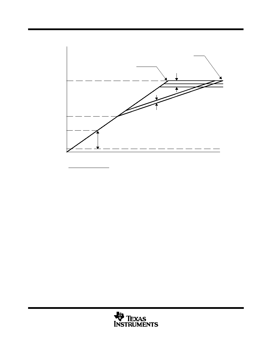
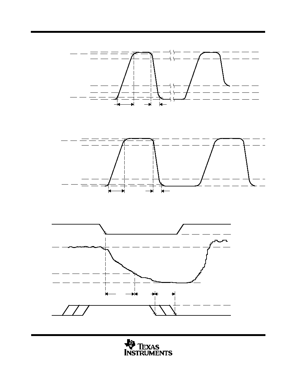
PARAMETER MEASUREMENT INFORMATION
DR (dynamic range)
+
camera white clip voltage
Vn
Vn = noise floor voltage
Vsat (min) = minimum saturation voltage
Vuse (max) = maximum usable voltage
Vuse (typ) = typical user voltage (camera white clip)
NOTES: A. Vuse (typ) is defined as the voltage determined to equal the camera white clip. This voltage must be less than Vuse (max).
B. A system trade-off is necessary to determine the system light sensitivity versus the signal/noise ratio. By lowering the Vuse (typ),
the light sensitivity of the camera is increased; however, this sacrifices the signal/noise ratio of the camera.
(light input)
Lux
Enabled
With Antiblooming
Blooming Point
Well Capacity
Dependent on
Disabled
With Antiblooming
Blooming Point
Gate High Level
Upon Antiblooming
Level Dependent
DR
Vn
Vsat (min)
Vuse (typ)
Vuse (max)
VO
Figure 16. Typical V
sat
, V
use
Relationship
TC217
1158-
×
488-PIXEL CCD IMAGE SENSOR
SOCS015C OCTOBER 1989 REVISED JUNE 1996
17
POST OFFICE BOX 655303
·
DALLAS, TEXAS 75265
PARAMETER MEASUREMENT INFORMATION
tf
tr
0%
VIL max
10%
Intermediate Level
VIH min
90%
100%
Slew rate between 10% and 90% = 70 to 120 V/
µ
s, tr = 150 ns, tf = 90 ns
Figure 17. Typical Clock Waveform for ABG, IAG, SAG1, SAG2, AND TMG
tf
tr
0%
VIL max
10%
VIH min
90%
100%
Slew rate between 10% and 90% = 300 V/
µ
s, tr = tf = 15 ns
Figure 18. Typical Clock Waveform for SRG1, SRG2, SRG3, and TRG
Sample
and
Hold
100%
90%
OUT
SRG
9 V
0%
9 V to 11 V
1.5 V to 2.5 V
CCD Delay
15 ns
10 ns
Figure 19. SRG and OUT Waveforms
TC217
1158-
×
488-PIXEL CCD IMAGE SENSOR
SOCS015C OCTOBER 1989 REVISED JUNE 1996
18
POST OFFICE BOX 655303
·
DALLAS, TEXAS 75265
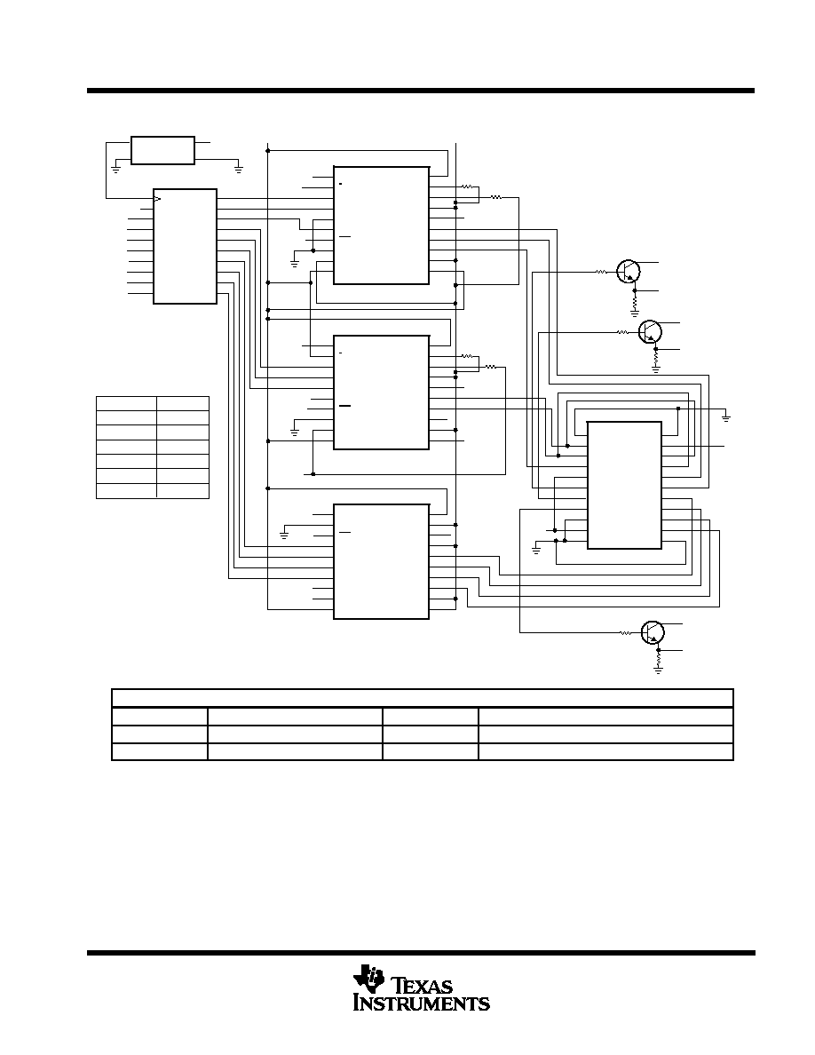
APPLICATION INFORMATION
16
15
13
12 V
SUB
TRG
SRG1
SRG2
SRG3
SAG2
TMG
IAG
ABG
TDB
SUB
SUB
CDB
AMP GND
OUT1
OUT2
OUT3
ADB
SAG1
IAG
ABG
SUB
12 V
OUT 3
1 k
100
OUT 2
12 V
12 V
13
14
15
16
17
18
19
20
21
22
12
11
10
9
8
7
6
5
4
3
2
1
Master Oscillator
GND
VCC
GND
OUT
VCC
VSS
User-Defined Timer
TRG
SRG1
SRG2
SRG3
GT
ABG
IAG
MEMA
TMG
MEMB
SH1
SH2
SH3
CSYNC
PC1
PC2
CBLNK
CLK
SH2
SH3
PC1
PC2
CBLNK
VSS
VSS
VCC
SEL1
VCC
TRGOUT
SRG1OUT
SRG2OUT
SRG3OUT
VCC
NC
SEL0
VSS
VSS
SEL1OUT
NC
TRGIN
SRG1IN
SRG2IN
SRG3IN
PD
GND
SEL0OUT
1
2
3
4
5
6
7
8
9
19
18
17
14
13
12
11
10
20
IALVL
I/N
IAIN
ABIN
MIDSEL
SAIN
PD
GND
IASR
ABSR
VCC
ABLVL
IAOUT
ABOUT
SAOUT
VCC
VABG
1
2
3
4
5
6
7
8
9
19
18
17
16
15
14
12
11
10
20
VABG
VCC
VCC
V
20
10
11
12
13
14
15
16
17
18
19
9
8
7
6
5
4
3
2
1
VABG
VCC
SAOUT
ABOUT
IAOUT
ABLVL
VCC
ABSR
IASR
GND
PD
SAIN
MIDSEL
ABIN
IAIN
I/N
IALVL
V
100
Parallel Driver
1 k
OUT 1
12 V
100
1 k
VABG +
47 k
20 k
47 k
20 k
ABLVL
PC3
PC3
CSYNC
SH1
2N3904
2N3904
2N3904
TC217
VSS
VSS
IALVL
VABG+
VABG+
TMS3473B
Parallel Driver
TMS3473B
SN28846
Serial Driver
Image Sensor
VCC
VSS
V
ABLVL
VABG +
VABG
IALVL
5 V
10 V
2 V
1.5 V
4 V
6 V
5 V
DC VOLTAGES
SUPPORT CIRCUITS
DEVICE
PACKAGE
APPLICATION
FUNCTION
SN28846DW
20 pin small outline
Serial driver
Driver for SRG1, SRG2, SRG3, and TRG
TMS3473BDW
20 pin small outline
Parallel driver
Driver for IAG, SAG1, SAG2, ABG, and TMG
Figure 20. Typical Application Circuit Diagram
TC217
1158-
×
488-PIXEL CCD IMAGE SENSOR
SOCS015C OCTOBER 1989 REVISED JUNE 1996
19
POST OFFICE BOX 655303
·
DALLAS, TEXAS 75265
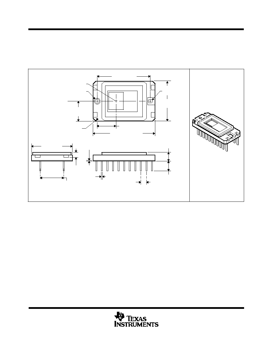
MECHANICAL DATA
The package for the TC217 consists of a ceramic base, a glass window, and a 22-lead frame. The package leads
are configured in a dual in-line organization and fit into mounting holes with 2.54 mm (0.10 inch) center-to-center
spacings. The glass window is sealed to the package by an epoxy adhesive. It can be cleaned by any standard
procedure for cleaning optical assemblies or by wiping the surface with a cotton swab moistened with alcohol.
(0.217
±
0.030)
5,50
±
0,76
3,86 (0.152) MAX
Optical Center
27,81 (1.095) MAX
8,00 (0.315)
23,39 (0.921)
0,25 (0.010)
10,16 (0.400) TYP
2,21 (0.087)
MAX
(0.730)
18,54
2,01 (0.079)
Index Dot
9,35 (0.368)
REF
0,46 (0.018)
2,54 (0.100)
18,24
(0.718)
2,01 x 2,39
(0.079 x 0.094)
ALL LINEAR DIMENSIONS ARE IN MILLIMETERS AND PARENTHETICALLY IN INCHES
C
L
Optical
(see Note B)
7/94
NOTES: A. Single dimensions are nominal.
B. The center of the package and the center of the image area are not coincident.
C. The distance from the top of the glass to the image sensor surface is typically 1,46 mm (0.057 inch). The glass is 0,95
±
0,08 mm
and has an index of refraction of 1.53.
D. Each pin centerline is located within 0,25 mm (0.010 inch) of its true longitudinal position.

488-PIXEL CCD IMAGE SENSOR
SOCS015C OCTOBER 1989 REVISED JUNE 1996
20
POST OFFICE BOX 655303
·
DALLAS, TEXAS 75265

IMPORTANT NOTICE
Texas Instruments and its subsidiaries (TI) reserve the right to make changes to their products or to discontinue
any product or service without notice, and advise customers to obtain the latest version of relevant information
to verify, before placing orders, that information being relied on is current and complete. All products are sold
subject to the terms and conditions of sale supplied at the time of order acknowledgement, including those
pertaining to warranty, patent infringement, and limitation of liability.
TI warrants performance of its semiconductor products to the specifications applicable at the time of sale in
accordance with TI's standard warranty. Testing and other quality control techniques are utilized to the extent
TI deems necessary to support this warranty. Specific testing of all parameters of each device is not necessarily
performed, except those mandated by government requirements.
CERTAIN APPLICATIONS USING SEMICONDUCTOR PRODUCTS MAY INVOLVE POTENTIAL RISKS OF
DEATH, PERSONAL INJURY, OR SEVERE PROPERTY OR ENVIRONMENTAL DAMAGE ("CRITICAL
APPLICATIONS"). TI SEMICONDUCTOR PRODUCTS ARE NOT DESIGNED, AUTHORIZED, OR
WARRANTED TO BE SUITABLE FOR USE IN LIFE-SUPPORT DEVICES OR SYSTEMS OR OTHER
CRITICAL APPLICATIONS. INCLUSION OF TI PRODUCTS IN SUCH APPLICATIONS IS UNDERSTOOD TO
BE FULLY AT THE CUSTOMER'S RISK.
In order to minimize risks associated with the customer's applications, adequate design and operating
safeguards must be provided by the customer to minimize inherent or procedural hazards.
TI assumes no liability for applications assistance or customer product design. TI does not warrant or represent
that any license, either express or implied, is granted under any patent right, copyright, mask work right, or other
intellectual property right of TI covering or relating to any combination, machine, or process in which such
semiconductor products or services might be or are used. TI's publication of information regarding any third
party's products or services does not constitute TI's approval, warranty or endorsement thereof.
Copyright
©
1998, Texas Instruments Incorporated