 | –≠–ª–µ–∫—Ç—Ä–æ–Ω–Ω—ã–π –∫–æ–º–ø–æ–Ω–µ–Ω—Ç: TC225-30 | –°–∫–∞—á–∞—Ç—å:  PDF PDF  ZIP ZIP |

TC221, TC225, TC227
SMALL-FORMAT CCD IMAGE SENSORS
SOCS037C ≠ DECEMBER 1991 ≠ REVISED AUGUST 1997
Copyright
©
1997, Texas Instruments Incorporated
1
POST OFFICE BOX 655303
∑
DALLAS, TEXAS 75265
∑
Full-Frame Operation
≠ 190 (H)
◊
190 (V) Active Elements for TC221
≠ 285 (H)
◊
285 (V) Active Elements for TC225
≠ 102 (H)
◊
102 (V) Active Elements for TC227
∑
Dark-Reference Pixels
∑
9-
µ
m Square Pixels
∑
Single-Phase Clocking
∑
Low Dark Current
∑
Dynamic Range . . . More Than 60 dB
∑
High Photoresponse Uniformity
∑
High Sensitivity
∑
Low-Noise Operation
∑
Solid State Reliability With No Residual
Imaging, Image Burn-In, Microphonics, or
Image Distortion
description
The TC221, TC225 and TC227 are full-frame
charge-coupled device (CCD) image sensors
designed specifically for medical and industrial
applications where ruggedness and small size are
required. The image-area diagonal measures
1.3 mm for the TC227, 2.4 mm for the TC221, and
3.63 mm for the TC225. The image sensors
contain, in addition to dark reference pixels, 190,
285, and 102 active lines with 190, 285, and 102
active pixels per line, respectively. The
antiblooming feature is activated by supplying
clock pulses to the antiblooming gate, an integral
part of each image-sensing element. The charge
is converted to signal voltage at 9.5
µ
V per
electron by a high-performance structure with
built-in automatic reset and a voltage-reference
generator. The signal is further buffered by a
low-noise two-stage source-follower amplifier to
provide high output-drive capability.
The TC221 and TC227 are supplied in 6-pin molded plastic packages; the TC225 is supplied in a 10-pin molded
plastic package. The glass window can be cleaned using any standard method for cleaning optical assemblies
or by wiping the surface with a cotton swab soaked in alcohol.
This MOS device contains limited built-in gate protection. During storage or handling, the device leads should be shorted together
or the device should be placed in conductive foam. In a circuit, unused inputs should always be connected to SUB. Under no
circumstances should pin voltages exceed absolute maximum ratings. Avoid shorting OUTn to ADB during operation to prevent
damage to the amplifier. The device can also be damaged if the output terminals are reverse-biased and an excessive current is
allowed to flow. Specific guidelines for handling devices of this type are contained in the publication
Guidelines for Handling
Electrostatic-Discharge-Sensitive (ESDS) Devices and Assemblies available from Texas Instruments.
TC225
TC221
TC227
10
9
8
7
6
1
2
3
4
5
1
2
3
6
5
4
SUB
OUT
ADB
SRG
ABG
IAG
TRG
SRG1
SRG2
ABG
IAG
SUB
OUT1
OUT2
ADB
NC
SRG
ABG
IAG
SUB
OUT
ADB
1
2
3
6
5
4
NC ≠ No internal connection
PRODUCTION DATA information is current as of publication date.
Products conform to specifications per the terms of Texas Instruments
standard warranty. Production processing does not necessarily include
testing of all parameters.

……
……
……
……
……
……
Dump Drain
217 Pixels
9
1
190
0.5
Optical
Black 1
ADB
OUT
SUB
190
Pixels
190
Lines
ABG
IAG
SRG
Top Drain
TC221
Dump Drain
ADB
OUT2
SUB
285
Pixels
285
Lines
ABG
IAG
SRG2
Top Drain
TC225
SRG1
OUT1
TRG
17
11
142.5
1.5
17
11.5
142.5
1
Dummy
Elements
Dummy
Elements
15.5
Optical
Black
TC221, TC225, TC227
SMALL-FORMAT CCD IMAGE SENSORS
SOCS037C ≠ DECEMBER 1991 ≠ REVISED AUGUST 1997
2
POST OFFICE BOX 655303
∑
DALLAS, TEXAS 75265
functional block diagrams

TC221, TC225, TC227
SMALL-FORMAT CCD IMAGE SENSORS
SOCS037C ≠ DECEMBER 1991 ≠ REVISED AUGUST 1997
3
POST OFFICE BOX 655303
∑
DALLAS, TEXAS 75265
functional block diagram
……
……
……
……
……
Dump Drain
129 Pixels
8
1
16.5
102
0.5
1
VCC
VO
SUB
ABG
IAG
SRG
Top Drain
TC227
Dummy
Elements
102
Lines
102
Pixels
TC221, TC225, TC227
SMALL-FORMAT CCD IMAGE SENSORS
SOCS037C ≠ DECEMBER 1991 ≠ REVISED AUGUST 1997
4
POST OFFICE BOX 655303
∑
DALLAS, TEXAS 75265
detailed description
The TC221, TC225, and TC227 consist of four basic functional blocks: (1) the image-sensing area, (2) the serial
registers, (3) the sensor node, and (4) the low-noise source-follower amplifier. The location of each of these
blocks is identified in the functional block diagrams.
image-sensing area
As light enters the silicon in the image-sensing area, free electrons are generated and collected in the potential
wells of the sensing elements. During this time, blooming protection is activated by applying a burst of pulses
to the antiblooming gate. This prevents blooming by the spilling of charge from overexposed elements into
neighboring elements. After integration and under dark conditions, the charge is transferred line by line into the
serial register(s). The required timing is shown in Figure 1 through Figure 3. During transfer, the antiblooming
gate is held at a low level. Each imager contains a specified number of dark pixels on the left side of the
image-sensing area. These elements provide the dark reference used in subsequent video-processing circuits
to restore the video black-level.
serial register(s)
Once an image line is transferred into the serial register, the serial-register gate can be clocked until all of the
charge packets are moved out onto the sense node. A drain is also included to provide the capability to clear
the image-sensing area of unwanted charge. Such charge can accumulate in the imager during the start-up of
operation or under special conditions when nonstandard TV operation is desired.
sense node(s) and source-follower amplifier(s)
After the charge packet is placed on the sense node, the potential of this node changes in proportion to the
amount of signal received. It is then buffered by a dual-stage source-follower amplifier. The sense node and
amplifier are located some distance from the serial register; a specified number of dummy elements is used to
span the distance. The location and number of the dummy elements are shown in the functional block diagrams.
Terminal Functions
TERMINAL
NAME
NUMBER
I/O
DESCRIPTION
NAME
TC221
TC225
TC227
ABG
2
4
5
I
Antiblooming gate
ADB
4
7
3
Amplifier-drain bias
IAG
3
5
4
I
Image-area gate
NC
N/A
6
N/A
No internal connection
OUT1
5
9
2
O
Output signal 1
OUT2
N/A
8
N/A
O
Output signal 2
SRG1
1
2
6
I
Serial-register gate 1
SRG2
N/A
3
N/A
I
Serial-register gate 2
SUB
6
10
1
Substrate
TRG
N/A
1
N/A
I
Transfer gate
N/A ≠ not applicable
TC221, TC225, TC227
SMALL-FORMAT CCD IMAGE SENSORS
SOCS037C ≠ DECEMBER 1991 ≠ REVISED AUGUST 1997
5
POST OFFICE BOX 655303
∑
DALLAS, TEXAS 75265
tw1
tw4
600 ns
tw3
600 ns
50 ns
t2
250 ns
tw1
125 ns
SRG
IAG
ABG
217 Cycles
SRG
IAG
Readout
Integration
190 Cycles
tw3
tw2
tw4
Figure 1. TC221 Timing Diagram
TC221, TC225, TC227
SMALL-FORMAT CCD IMAGE SENSORS
SOCS037C ≠ DECEMBER 1991 ≠ REVISED AUGUST 1997
6
POST OFFICE BOX 655303
∑
DALLAS, TEXAS 75265
tw2
tw1
tw3
TRG
SRG2
SRG1
ABG
IAG
Readout
Integration
285 Cycles
172 Cycles
172 Cycles
IAG
TRG
tw1
600 ns
tw2
600 ns
tw3
600 ns
tw4
125 ns
tw4
SRG1
SRG2
Figure 2. TC225 Timing Diagram

TC221, TC225, TC227
SMALL-FORMAT CCD IMAGE SENSORS
SOCS037C ≠ DECEMBER 1991 ≠ REVISED AUGUST 1997
7
POST OFFICE BOX 655303
∑
DALLAS, TEXAS 75265
tw1
tw4
600 ns
tw3
600 ns
50 ns
t2
250 ns
tw1
125 ns
SRG
IAG
ABG
129 Cycles
SRG
IAG
Readout
Integration
102 Cycles
tw3
tw2
tw4
Figure 3. TC227 Timing Diagram
SRG
CCD
QR
Q2
Q1
Q4
Q3
C0
Q5
Q7
VO
VRF
VDD
SUB
Q6
Figure 4. Charge-Detection Schematic

TC221, TC225, TC227
SMALL-FORMAT CCD IMAGE SENSORS
SOCS037C ≠ DECEMBER 1991 ≠ REVISED AUGUST 1997
8
POST OFFICE BOX 655303
∑
DALLAS, TEXAS 75265
spurious-nonuniformity specification
The spurious-nonuniformity specification of the TC221, TC225 and TC227 grades ≠ 30 and ≠ 40 is based on
several sensor characteristics:
∑
Amplitude of the nonuniform pixel
∑
Polarity of the nonuniform pixel
-- Black
-- White
∑
Location of the nonuniformity (see Figure 5)
∑
Nonuniform pixel count
The CCD sensors are characterized in both an illuminated condition and a dark condition. In the dark condition,
the nonuniformity is specified in terms of absolute amplitude as shown in Figure 6. In the illuminated condition,
the nonuniformity is specified as a percentage of the total illumination as shown in Figure 7.
TC221 nonuniformity table
DARK CONDITION
ILLUMINATED CONDITION
PART NUMBER
PIXEL
PIXEL COUNT
% OF TOTAL
PIXEL COUNT
AMPLITUDE
AREA A
AREA B
ILLUMINATION
AREA A
AREA B
TC221-30
8 12 mV
4
6
30 40
4
6
TC221-40
8 ≠12 mV
8
12
30 ≠ 40
8
12
TC221-30
12 16 mV
2
4
40 50
2
4
TC221-40
12 ≠16 mV
4
8
40 ≠ 50
4
8
TC221-30
> 16 mV
0
0
> 50
0
0
TC221-40
> 16 mV
0
0
> 50
0
0
TC225 nonuniformity table
DARK CONDITION
ILLUMINATED CONDITION
PART NUMBER
PIXEL
PIXEL COUNT
% OF TOTAL
PIXEL COUNT
AMPLITUDE
AREA A
AREA B
ILLUMINATION
AREA A
AREA B
TC225-30
8 12 mV
6
9
30 40
6
9
TC225-40
8 ≠12 mV
12
15
30 ≠ 40
12
15
TC225-30
12 16mV
3
6
40 50
3
6
TC225-40
12 ≠16mV
6
10
40 ≠ 50
6
10
TC225-30
> 16 mV
0
0
> 50
0
0
TC225-40
> 16 mV
0
0
> 50
0
0
TC227 nonuniformity table
DARK CONDITION
ILLUMINATED CONDITION
PART NUMBER
PIXEL
PIXEL COUNT
% OF TOTAL
PIXEL COUNT
AMPLITUDE
AREA A
AREA B
ILLUMINATION
AREA A
AREA B
TC227-30
8 12 mV
4
6
30 40
4
6
TC227-40
8 ≠12 mV
8
12
30 ≠ 40
12
12
TC227-30
12 16 mV
2
4
40 50
2
4
TC227-40
12 ≠16 mV
4
8
40 ≠ 50
4
8
TC227-30
> 16 mV
0
0
> 50
0
0
TC227-40
> 16 mV
0
0
> 50
0
0

TC221, TC225, TC227
SMALL-FORMAT CCD IMAGE SENSORS
SOCS037C ≠ DECEMBER 1991 ≠ REVISED AUGUST 1997
9
POST OFFICE BOX 655303
∑
DALLAS, TEXAS 75265
H
V
1/2 V
1/2 H
Area A
Area B
Figure 5. Area Location Map
t
t
mV
Amplitude
% of T
otal
Illumination
Figure 6. Pixel Nonuniformity,
Figure 7. Pixel Nonuniformity,
Dark Condition
Illuminated Condition
TC221, TC225, TC227
SMALL-FORMAT CCD IMAGE SENSORS
SOCS037C ≠ DECEMBER 1991 ≠ REVISED AUGUST 1997
10
POST OFFICE BOX 655303
∑
DALLAS, TEXAS 75265
absolute maximum ratings over operating free-air temperature range (unless otherwise noted)
Supply voltage range V
CC
for ADB (see Note 1)
0 V to 15 V
. . . . . . . . . . . . . . . . . . . . . . . . . . . . . . . . . . . . . . . . .
Input voltage range V
I
for ABG, IAG, SRG, TRG
≠ 15 V to 15 V
. . . . . . . . . . . . . . . . . . . . . . . . . . . . . . . . . . . . . .
Operating free-air temperature range, T
A
≠ 10
∞
C to 60
∞
C
. . . . . . . . . . . . . . . . . . . . . . . . . . . . . . . . . . . . . . . . . . . .
Storage temperature range
≠ 30
∞
C to 85
∞
C
. . . . . . . . . . . . . . . . . . . . . . . . . . . . . . . . . . . . . . . . . . . . . . . . . . . . . . . . .
Stresses beyond those listed under "absolute maximum ratings" may cause permanent damage to the device. These are stress ratings only, and
functional operation of the device at these or any other conditions beyond those indicated under "recommended operating conditions" is not
implied. Exposure to absolute-maximum-rated conditions for extended periods may affect device reliability.
NOTE 1: All voltage values are with respect to the substrate.
recommended operating conditions
MIN
NOM
MAX
UNIT
Supply voltage, VCC
ADB
11
12
13
V
Substrate bias voltage
0
V
IAG
High level
1.5
2
2.5
IAG
Low level
≠ 11
≠ 10
≠ 9
SRG
High level
1.5
2
2.5
SRG
Low level
≠ 11
≠ 10
≠ 9
Input voltage, VI
High level
11
V
ABG
Intermediate levelß
≠ 3
Low level
≠ 6
TRG
High level
1.5
2
2.5
TRG
Low level
≠ 11
≠ 10
≠ 9
Pulse duration
IAG
0.7
1.0
1.3
µ
s
Clock frequency f l k
SRG, TRG
10
MHz
Clock frequency, fclock
ABG
4
MHz
Load capacitance
6
pF
Operating free-air temperature, TA
≠ 10
45
∞
C
The algebraic convention, in which the least positive (most negative) value is designated minimum, is used in this data sheet for clock voltage
levels.
ß The antiblooming gate clocks from high level to intermediate level during exposure time and is held at low level during readout time.
TC221, TC225, TC227
SMALL-FORMAT CCD IMAGE SENSORS
SOCS037C ≠ DECEMBER 1991 ≠ REVISED AUGUST 1997
11
POST OFFICE BOX 655303
∑
DALLAS, TEXAS 75265
electrical characteristics over recommended operating ranges of supply voltage and operating
free-air temperature (unless otherwise noted)
PARAMETER
MIN
TYP
MAX
UNIT
Dynamic range (see Note 2)
60
dB
Charge-conversion factor
9.5
µ
V/e
Charge-transfer efficiency (see Note 3)
0.99990
1.00000
Signal-response delay (see Note 4)
30
ns
Gamma (see Note 5)
0.90
1.0
Noise-equivalent signal (KTC noise without CDS circuit)
36
e
Output resistance
600
ADB (see Note 6)
≠ 20
Rejection ratio
SRG (see Note 7)
≠ 40
dB
ABG (see Note 8)
≠ 50
Supply current
5
mA
IAG
600
Input capacitance, Ci (TC221)
SRG
20
pF
ABG
240
IAG
1320
Input capacitance Ci (TC225)
SRG1, SRG2
40
pF
Input capacitance, Ci (TC225)
TRG
60
pF
ABG
520
IAG
200
Input capacitance, Ci (TC227)
SRG
10
pF
ABG
100
All typical values are at TA = 25
∞
C.
NOTES:
2. Dynamic range is ≠ 20 times the logarithm of the mean-noise signal divided by the saturation-output signal.
3. Charge-transfer efficiency is 1 minus the charge loss per transfer in the output register. The test is performed in the dark using an
electrical-input signal.
4. Signal-response delay time is the time between the falling edge of the SRG clock pulse and the output-signal valid state.
5. Gamma (
) is the value of the exponent in the equation below for two points on the linear portion of the transfer-function curve (this
value represents points near saturation):
Exposure (2)
Exposure (1)
g
+
Output signal (2)
Output signal (1)
6. ADB rejection ratio is ≠ 20 times the logarithm of the ac amplitude at the output divided by the ac amplitude at ADB.
7. SRG rejection ratio is ≠ 20 times the logarithm of the ac amplitude at the output divided by the ac amplitude at SRG.
8. ABG rejection ratio is ≠ 20 times the logarithm of the ac amplitude at the output divided by the ac amplitude at ABG.
optical characteristics, T
A
= 25
∞
C, integration time = 16.67 ms (unless otherwise noted)
PARAMETER
MIN
TYP
MAX
UNIT
Sensitivity (see Note 9)
No IR Filter
210
mV/lx
Sensitivity (see Note 9)
With IR Filter
30
mV/lx
Saturation signal (see Note 10)
350
380
400
mV
Maximum usable signal
170
190
200
mV
Blooming overload ratio (see Note 11)
5
Image-area well capacity
40
ke
Dark current
TA = 21
∞
C
0.27
nA/cm2
Dark signal uniformity
TA = 45
∞
C
10
mV
Shading
Output signal = 100 mV
20%
NOTES:
9. Sensitivity is measured at a source temperature of 2856 K. A 1-mm CM-500 filter is used.
10. Saturation is the condition in which further increase in exposure does not lead to further increase in output signal.
11. Blooming-overload ratio is the ratio of blooming exposure to saturation exposure.
TC221, TC225, TC227
SMALL-FORMAT CCD IMAGE SENSORS
SOCS037C ≠ DECEMBER 1991 ≠ REVISED AUGUST 1997
12
POST OFFICE BOX 655303
∑
DALLAS, TEXAS 75265
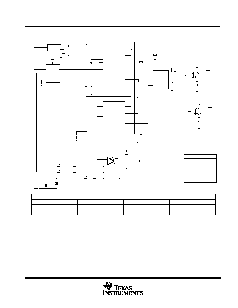
APPLICATION INFORMATION
OUT2
2N3904
Q2
12 V
TC225
12 V
100
R11
OUT1
2N3904
Q1
12 V
NC
ADB
OUT2
OUT1
SUB
IAG
ABG
SRG2
SRG1
TRG
SN28846
VCC
+
V
+
+
VSS
1N4148
5 k
R5
+
68
µ
F
C10
≠12 V
1 k
R9
D1
D2
1N4148
300
R8
1 k
R10
EL2020
4
2
3
7
15 V
≠15 V
5
6
8
1
≠
+
TMS3473B
+
IALVL
I/N
IAIN
ABIN
MIDSEL
SAIN
PD
GND
Vabg+
IASR
ABSR
V
ABLVL
IAOUT
ABOUT
SAOUT
VCC
Vabg≠
1
2
3
4
5
6
7
8
9
19
18
17
16
15
14
13
12
11
11
12
13
14
15
16
17
18
19
9
8
7
6
5
4
3
2
1
SEL1
VCC
TRGOUT
SRG1OUT
SRG2OUT
SRG3OUT
VCC
NC
SEL0
SEL2OUT
NC
TRGIN
SRG1IN
SRG2IN
SRG3IN
PD
GND
SEL1OUT
Master Oscillator
GND
+5 V
OUT
IAG
TG
SG1
SG2
VCC
GND
ABL
ABM
ABH
CLK
VCC
VCC
VCC
VSS
VCC
+
VCC
C1
0.1
µ
F
User-Defined Timer
ADB
VCC
VSS
V
ABLVL
VABG +
VABG ≠
12 V
5 V
≠ 10 V
2 V
≠ 2.5 V
4 V
≠ 6 V
DC VOLTAGES
C2
0.1
µ
F
C3
68
µ
F
C4
68
µ
F
C11
0.1
µ
F
1 k
R12
C10
0.1
µ
F
C12
0.1
µ
F
100
R13
1 k
R14
C5
68
µ
F
22 k
R1
22 k
R2
C6
68
µ
F
C8
0.1
µ
F
C9
0.1
µ
F
200
R7
500
R3
70
R4
1.5
R6
C7
68
µ
F
10
VSS
20
VSS
VSS
10
20
VSS
VABG≠
ABLVL
VABG+
SUPPORT CIRCUITS
DEVICE
PACKAGE
APPLICATION
FUNCTION
SN28846DW
20 pin small outline
Serial driver
Driver for SRG
TMS3473BDW
20 pin small outline
Parallel driver
Driver for IAG
Figure 8. Typical Application Circuit Diagram

TC221, TC225, TC227
SMALL-FORMAT CCD IMAGE SENSORS
SOCS037C ≠ DECEMBER 1991 ≠ REVISED AUGUST 1997
13
POST OFFICE BOX 655303
∑
DALLAS, TEXAS 75265
MECHANICAL DATA
…
…
……
……
……
……
……
……
……
……
……
……
……
……
……………
…
…
…
…
…
………………
………………
…
…
…
…
…
…
…
…
…
…
…
…
…
…
…
…
…
…
TC221
3,30 (0.130)
3,10 (0.122)
2,70 (0.106)
2,40 (0.094)
2,50 (0.098)
2,30 (0.091)
1,20 (0.047)
NOM
4,20 (0.165)
NOM
3,60 (0.142)
NOM
3,50 (0.138)
NOM
ALL LINEAR DIMENSIONS ARE IN MILLIMETERS AND PARENTHETICALLY IN INCHES
TC227
TC225
2,70 (0.106)
2,45 (0.096)
1,70 (0.067)
1,45 (0.057)
1
2
3
6
5
4
1
2
3
6
5
4
1
2
3
4
5
10
9
8
7
6
2,00 (0.079)
NOM
7/94

IMPORTANT NOTICE
Texas Instruments and its subsidiaries (TI) reserve the right to make changes to their products or to discontinue
any product or service without notice, and advise customers to obtain the latest version of relevant information
to verify, before placing orders, that information being relied on is current and complete. All products are sold
subject to the terms and conditions of sale supplied at the time of order acknowledgement, including those
pertaining to warranty, patent infringement, and limitation of liability.
TI warrants performance of its semiconductor products to the specifications applicable at the time of sale in
accordance with TI's standard warranty. Testing and other quality control techniques are utilized to the extent
TI deems necessary to support this warranty. Specific testing of all parameters of each device is not necessarily
performed, except those mandated by government requirements.
CERTAIN APPLICATIONS USING SEMICONDUCTOR PRODUCTS MAY INVOLVE POTENTIAL RISKS OF
DEATH, PERSONAL INJURY, OR SEVERE PROPERTY OR ENVIRONMENTAL DAMAGE ("CRITICAL
APPLICATIONS"). TI SEMICONDUCTOR PRODUCTS ARE NOT DESIGNED, AUTHORIZED, OR
WARRANTED TO BE SUITABLE FOR USE IN LIFE-SUPPORT DEVICES OR SYSTEMS OR OTHER
CRITICAL APPLICATIONS. INCLUSION OF TI PRODUCTS IN SUCH APPLICATIONS IS UNDERSTOOD TO
BE FULLY AT THE CUSTOMER'S RISK.
In order to minimize risks associated with the customer's applications, adequate design and operating
safeguards must be provided by the customer to minimize inherent or procedural hazards.
TI assumes no liability for applications assistance or customer product design. TI does not warrant or represent
that any license, either express or implied, is granted under any patent right, copyright, mask work right, or other
intellectual property right of TI covering or relating to any combination, machine, or process in which such
semiconductor products or services might be or are used. TI's publication of information regarding any third
party's products or services does not constitute TI's approval, warranty or endorsement thereof.
Copyright
©
1999, Texas Instruments Incorporated