TC271
1080
◊
580-PIXEL CCD IMAGE SENSOR
SOCS039A ≠ JANUARY 1994 ≠ REVISED JUNE 1996
Copyright
©
1996, Texas Instruments Incorporated
1
POST OFFICE BOX 655303
∑
DALLAS, TEXAS 75265
∑
High-Resolution, Solid-State Monochrome
Image Sensor for Video or Still-Picture
Photography
∑
Frame Transfer With Two Field Memories
Allows Multimode Operation
∑
1044 (H) x 576 (V) Active Elements in
Image-Sensing Area
∑
11-mm Image-Area Diagonal Is Compatible
With 2/3" Vidicon Optics
∑
Fast-Clear Capability
∑
Electron-Hole Recombination Antiblooming
∑
Dynamic Range . . . More Than 60 dB
∑
High Photoresponse Uniformity
∑
On-Chip Cross-Coupled Resets for Easy
Off-Chip Implementation of CCSH Video-
Signal Processing
∑
Solid-State Reliability With No Image
Burn-in, Residual Imaging, Image
Distortion, Image Lag, or Microphonics
∑
Low Dark Current
description
The TC271 is a frame-transfer charge-coupled-device (CCD) image sensor with two field memories. It is
suitable for use in PAL-video or still-picture photography applications. Its image-sensing area is configured into
580 lines; 576 of these are active and the remaining four are used for dark reference. Each line is configured
into 1080 pixels with 1044 active and 36 for dark reference. The TC271 has a standard aspect ratio of 4:3 and
a standard 11-mm image-sensing-area diagonal. Its blooming protection, which is an integral part of each pixel,
is based on electron-hole recombination and is activated by clocking the antiblooming gate.
One important aspect of the TC271 high-resolution sensor is its ability to simultaneously capture both fields of
a TV frame. Its two independently addressable memories allow separate storage of each field and operation
in a variety of modes, including CCIR with true interlace, CCIR with pseudointerlace, progressive scan, and
nonstandard pseudointerlace with a resolution of 1152 lines.
A unique multiplexer section (see Figure 1) rearranges the horizontal pixels into vertical groups of three and
separates and loads the image into the two field memories. The independent addressing of each field memory
provides flexibility for different modes of operation. The interdigitated layout of the memories allows each
memory to share the same bank of three serial registers and associated charge-detection amplifiers (see
Figure 2 and the functional block diagram). Each register and associated amplifier reads out every third column
of the image area (see Figure 3). The three amplifiers are optimized dual-source followers that allow the use
of off-chip double correlated-clamp sample-and-hold amplifiers for removing KTC noise.
The TC271 is built using TI-proprietary virtual-phase technology, which provides devices with high blue
response, low dark current, high photoresponse uniformity, and single-phase clocking. The TC271 is
characterized for operation from ≠10
∞
C to 40
∞
C.
This MOS device contains limited built-in gate protection. During storage or handling, the device leads should be shorted together
or the device should be placed in conductive foam. In a circuit, unused inputs should always be connected to SUB. Under no
circumstances should pin voltages exceed absolute maximum ratings. Avoid shorting OUTn to ADB during operation to prevent
damage to the amplifier. The device can also be damaged if the output terminals are reverse-biased and an excessive current is
allowed to flow. Specific guidelines for handling devices of this type are contained in the publication
Guidelines for Handling
Electrostatic-Discharge-Sensitive (ESDS) Devices and Assemblies available from Texas Instruments.
SUB
CDB
AMP GND
OUT1
OUT2
OUT3
ADB
SAG1
IAG
ABG
SUB
SUB
TRG
SRG1
SRG2
SRG3
SAG2
TMG
IAG
ABG
TDB
SUB
22
21
20
19
18
17
16
15
14
13
12
11
10
9
8
7
6
5
4
3
2
1
DUAL-IN-LINE PACKAGE
(TOP VIEW)
ADVANCE INFORMATION concerns new products in the sampling or
preproduction phase of development. Characteristic data and other
specifications are subject to change without notice.

TC271
1080
◊
580-PIXEL CCD IMAGE SENSOR
SOCS039A ≠ JANUARY 1994 ≠ REVISED JUNE 1996
4
POST OFFICE BOX 655303
∑
DALLAS, TEXAS 75265
Terminal Functions
TERMINAL
I/O
DESCRIPTION
NAME
NO.
I/O
DESCRIPTION
ABG
2
I
Antiblooming gate
ABG
20
I
Antiblooming gate
ADB
5
I
Supply voltage for amplifier-drain bias
AMP GND
9
Amplifier ground
CDB
10
I
Supply voltage for clearing-drain bias
IAG
3
I
Image-area gate
IAG
19
I
Image-area gate
OUT1
8
O
Output signal 1
OUT2
7
O
Output signal 2
OUT3
6
O
Output signal 3
SAG1
4
I
Storage-area gate
SAG2
17
I
Storage-area gate
SRG1
14
I
Serial-register gate 1
SRG2
15
I
Serial-register gate 2
SRG3
16
I
Serial-register gate 3
SUB
1
Substrate and clock return
SUB
11
Substrate and clock return
SUB
12
Substrate and clock return
SUB
22
Substrate and clock return
TDB
21
I
Supply voltage for top-drain bias
TMG
18
I
Transfer-multiplex gate
TRG
13
I
Transfer gate
All pins of the same name should be connected together externally (i.e., pin 2 to pin 20,
pin 3 to pin 19, etc.).
detailed description
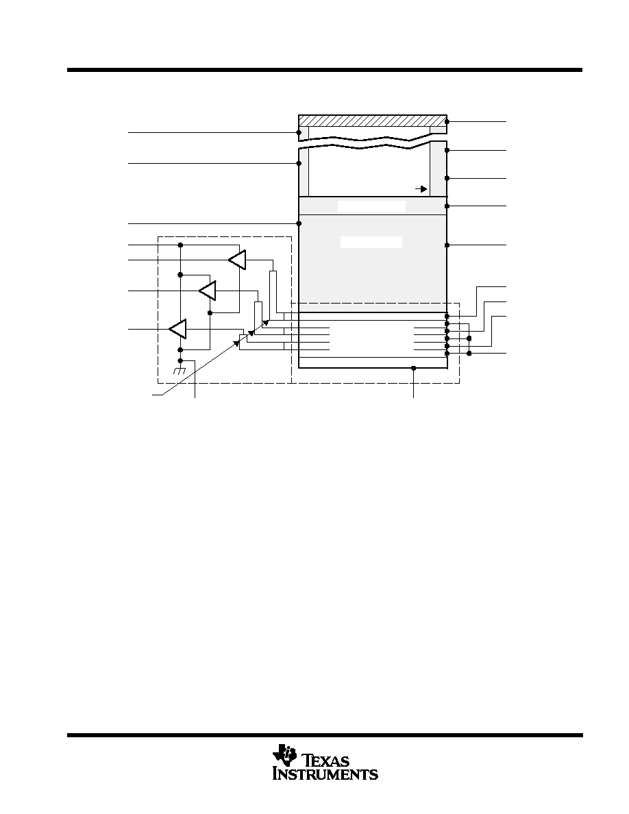
The TC271 consists of five basic functional blocks: (1) the image-sensing area, (2) the multiplexer block, (3)
the image-storage area with dual-field memories, (4) the serial-register and transfer gates, and (5) the low-noise
signal-processing amplifier block with charge-detection nodes. The location of each of these blocks is identified
in the functional block diagram.
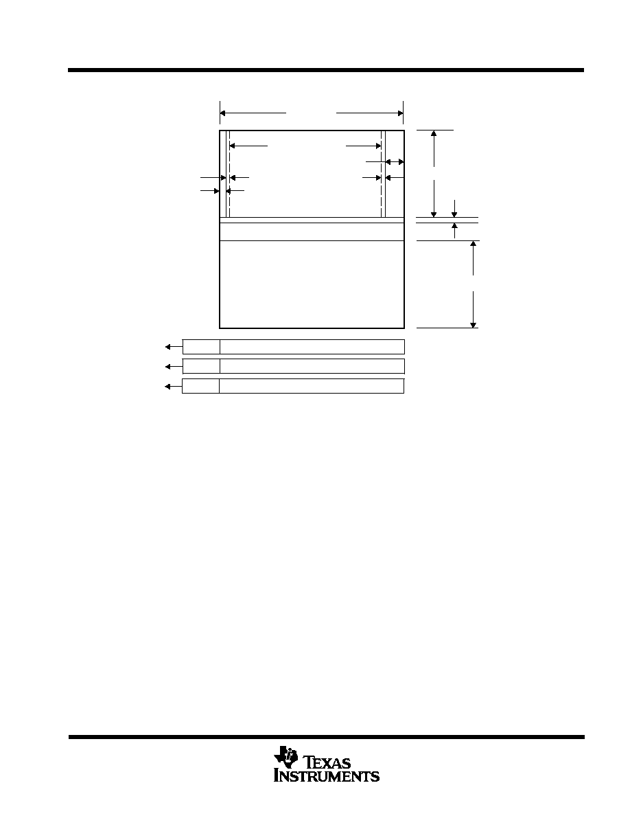
image-sensing area
Figure 4 and Figure 5 show cross sections with potential-well diagrams and top views of image-sensing
elements. As light enters the silicon in the image-sensing area, free electrons are generated and collected in
the potential wells of the sensing elements. During this time, blooming protection is activated by applying a burst
of pulses to the antiblooming-gate inputs every horizontal-blanking interval. This prevents blooming caused by
the spilling of charge from overexposed elements into neighboring elements. Thirty-four full columns and one
half-column of elements at the right edge of the image-sensing area are shielded from incident light; these
elements provide the dark reference used in subsequent video-processing circuits to restore the video-black
level. There are also one full column and one half-column of light-shielded elements at the left edge of the
image-sensing area and four lines of light-shielded elements at the bottom of the image area immediately above
the multiplexer. The latter prevent charge leakage from the image area into the multiplexer.

TC271
1080
◊
580-PIXEL CCD IMAGE SENSOR
SOCS039A ≠ JANUARY 1994 ≠ REVISED JUNE 1996
5
POST OFFICE BOX 655303
∑
DALLAS, TEXAS 75265
multiplexer and image-storage area
After integration, the multiplexer rearranges two horizontal lines into vertical groups of three and separates and
loads the image into the storage area. Figure 1 shows the layout of the multiplexer gate and its interface to the
two field memories. Figure 2 shows the interface region between the storage area and the three serial registers.
A drain is also provided to clear the image-sensing and image-storage areas of unwanted charge. Such charge
can accumulate in the imager during the startup of operation or under special circumstances when nonstandard
TV operation is desired. The sensor's independently addressable memories allow several different modes of
sensor operation including (1) a normal-light mode, (2) a low-light mode, (3) a still mode, and (4) a
progressive-scan mode. The timing for these four modes is given in Figure 6 through Figure 9. The
parallel-transfer timing is shown in Figure 10.
serial registers and amplifiers
After transfer to the serial registers (see Figure 11, which shows the horizontal timing that gives the necessary
sequence of pulses for transfer from the storage area to the serial registers), the charge is converted to a signal
voltage at the sense node and buffered with a dual-stage source follower. The three serial registers are typically
clocked 120 degrees out of phase with each serial-gate pulse supplying a detection-node reset signal for one
of the other two serial gates (see Figure 12). The readout timing, which includes the three serial pulses and the
pixel-clamp pulses used in an off-chip double-correlated sampling circuit, is shown in Figure 13. The detection
nodes and amplifiers are located some distance from the edge of the storage area. Twelve dummy elements
are incorporated at the end of each serial register to span the distance. The location of the dummy elements,
which are considered to be part of the amplifiers, is shown in the functional block diagram. A schematic of the
detection node and amplifier is given in Figure 3.