 | –≠–ª–µ–∫—Ç—Ä–æ–Ω–Ω—ã–π –∫–æ–º–ø–æ–Ω–µ–Ω—Ç: TCM1520AD | –°–∫–∞—á–∞—Ç—å:  PDF PDF  ZIP ZIP |
TCM1520A
RING DETECTOR
SCTS005B ≠ OCTOBER 1984 ≠ REVISED DECEMBER 1990
Copyright
©
1990, Texas Instruments Incorporated
1
POST OFFICE BOX 655303
∑
DALLAS, TEXAS 75265
POST OFFICE BOX 1443
∑
HOUSTON, TEXAS 77251≠1443
∑
On-Chip 150-V Bridge Diode Configuration
∑
Reliable BIDFET
Technology
∑
High Standby Impedance . . . 1 M
Typ
∑
Efficient High-Voltage Operation
∑
Output Compatible With TTL, NMOS, and
CMOS
∑
Built-In 5-V Series Regulator
∑
Built-In Lightning and Transient Protection
description
The TCM1520A is a monolithic ring-detection
integrated circuit designed for use in isolated or
nonisolated telephone applications. The device
uses a modified form of the Texas Instruments
BIDFET
technology to combine low-voltage
CMOS and high-voltage bipolar input/output
circuitry. It features efficient high-voltage (40 V to
150 V) operation with a typical current drain of
1 mA.
During standby, the input impedance is
approximately 1 M
or greater, which prevents
any interference with parallel off-hook telephones
transmitting DTMF or voice frequencies. The
device achieves this high input impedance with an
on-chip series zener diode that does not conduct
until the voltage across AC INPUT (pins 1 and 8)
exceeds 8 V. When the voltage across pins 1 and
8 exceeds 18 V, the internal switch is closed, which bypasses the 6.8-V zener diode series resistor. This allows
more efficient power transfer to the load when the device is in the operating mode. In the operating mode, the
impedance of the device varies from 30 k
to 7 k
over the ring signal of 40 V at 16 Hz to 150 V at 68 Hz and
is reasonably independent of the output load.
In typical telephone applications, the TCM1520A is activated through the telephone line by a ring voltage of 40 V
at 16 Hz to 150 V at 68 Hz. The TCM1520A generates a signal suitable to drive an optocoupler or TTL, NMOS,
or CMOS logic. The 5-V OUTPUT can be used as a supply source for optocouplers or low-power logic. This
output is noninverting and is at a high level during ringing.
The TCM1520A incorporates lightning and transient protection that is designed to withstand lightning strikes
of 1.5-kV amplitude and 200-
µ
s duration and also features built-in circuitry to avoid tapping or false triggering
due to transients.
Caution. These devices have limited built-in ESD protection. The leads should be shorted together or the device placed in conductive
foam during storage or handling to prevent electrostatic damage to the MOS gates.
BIDFET ≠ Bipolar, double-diffused, N-channel and P-channel MOS transistors on same chip. This is a patented process.
1
2
3
4
8
7
6
5
AC INPUT
INVERTING OUTPUT
COMMON
5-V OUTPUT
AC INPUT
COMMON
C FILTER
BELL TAPPING SENSE
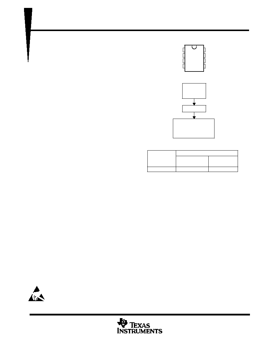
D OR P PACKAGE
(TOP VIEW)
TCM1520A APPLICATION
Phone Line
AC Ring
Signal
TCM1520A
Electronic Telephone
or Accessory
TTL /NMOS/CMOS
Microprocessor
AVAILABLE OPTIONS
PACKAGE
SMALL OUTLINE
(D)
PLASTIC DIP
(P)
TCM1520AD
TCM1520AP
≠ 40
∞
C to 85
∞
C
TA
The D package is available taped and reeled with suffix R
added to the device type (i.e., TCM1520ADR).
PRODUCTION DATA information is current as of publication date.
Products conform to specifications per the terms of Texas Instruments
standard warranty. Production processing does not necessarily include
testing of all parameters.
TCM1520A
DUAL DIFFERENTIAL COMPARATORS
SCTS005B ≠ OCTOBER 1984 ≠ REVISED DECEMBER 1990
2
POST OFFICE BOX 655303
∑
DALLAS, TEXAS 75265
POST OFFICE BOX 1443
∑
HOUSTON, TEXAS 77251≠1443
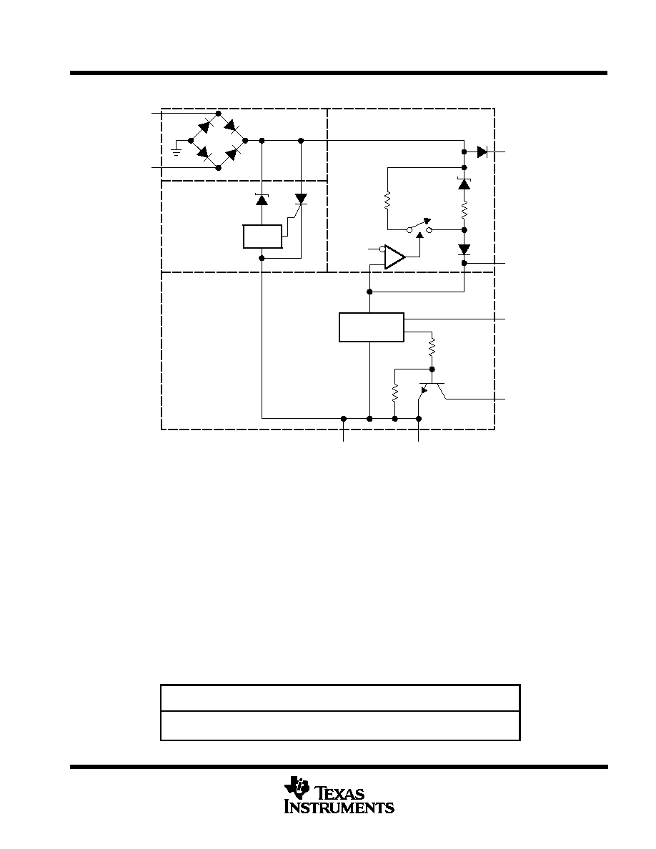
functional block diagram
Current
Sensor
Ring-Signal
Voltage Input
Section
Vref
200
6.8 V
8 k
5-V Series
Regulator
18 k
Transient
Protection
Section
45 V
1A
5
6
4
2
1
8
3
7
COMMON
COMMON
BELL TAPPING
SENSE
C FILTER
5-V OUTPUT
INVERTING
OUTPUT
AC INPUT
AC INPUT
Regulated
Voltage
Output Section
High-Input Impedance/
Antitapping Section
absolute maximum ratings over operating free-air temperature range (unless otherwise noted)
Continuous supply voltage at C FILTER (see Note 1)
40 V
. . . . . . . . . . . . . . . . . . . . . . . . . . . . . . . . . . . . . . . . . .
Continuous differential input voltage, V
ID
(AC INPUT)
40 V
. . . . . . . . . . . . . . . . . . . . . . . . . . . . . . . . . . . . . . . . .
Continuous output current at 5-V OUTPUT, I
O
12 mA
. . . . . . . . . . . . . . . . . . . . . . . . . . . . . . . . . . . . . . . . . . . . . . .
Continuous SCR on-state input current
200 mA
. . . . . . . . . . . . . . . . . . . . . . . . . . . . . . . . . . . . . . . . . . . . . . . . . . . .
SCR on-state input current, I
I(on)
(duration
200
µ
s)
900 mA
. . . . . . . . . . . . . . . . . . . . . . . . . . . . . . . . . . . . . . . . .
Continuous total dissipation
See Dissipation Rating Table
. . . . . . . . . . . . . . . . . . . . . . . . . . . . . . . . . . . . . . . . . . .
Operating free-air temperature range, T
A
≠ 40
∞
C to 105
∞
C
. . . . . . . . . . . . . . . . . . . . . . . . . . . . . . . . . . . . . . . . . .
Storage temperature range
≠ 40
∞
C to 125
∞
C
. . . . . . . . . . . . . . . . . . . . . . . . . . . . . . . . . . . . . . . . . . . . . . . . . . . . . . .
Lead temperature 1,6 mm (1/16 inch) from case for 10 seconds
260
∞
C
. . . . . . . . . . . . . . . . . . . . . . . . . . . . . . .
Stresses beyond those listed under "absolute maximum ratings" may cause permanent damage to the device. These are stress ratings only, and
functional operation of the device at these or any other conditions beyond those indicated under "recommended operating conditions" is not
implied. Exposure to absolute-maximum-rated conditions for extended periods may affect device reliability.
NOTE 1: All voltage values, unless otherwise noted, are with respect to COMMON (pin 7).
DISSIPATION RATING TABLE
PACKAGE
TA = 25
∞
C
POWER RATING
OPERATING FACTOR
ABOVE TA = 25
∞
C
TA = 85
∞
C
POWER RATING
D
950 mW
7.6 mW/
∞
C
494 mW
P
1000 mW
8.0 mW/
∞
C
520 mW
TCM1520A
RING DETECTOR
SCTS005B ≠ OCTOBER 1984 ≠ REVISED DECEMBER 1990
3
POST OFFICE BOX 655303
∑
DALLAS, TEXAS 75265
POST OFFICE BOX 1443
∑
HOUSTON, TEXAS 77251≠1443
recommended operating conditions
MIN
MAX
UNIT
Input voltage, VIrms (f = 15.3 Hz to 68 Hz) (see Note 2)
40
150
V
Operating free-air temperature, TA
≠ 40
85
∞
C
NOTE 2: Input voltage is applied to AC INPUT (pins 1 and 8) through a series 2.2-k
±
10% resistor and a 0.47-
µ
F
±
10% capacitor. (see
Figures 1, 4, and 5.)
electrical characteristics over recommended operating free-air temperature range, R
L
= open,
C
(fltr)
= 10
µ
F (unless otherwise noted)
detector section
PARAMETER
TEST CONDITIONS
MIN
TYP
MAX
UNIT
V(BR) CEX
Collector-emitter output breakdown voltage,
INVERTING OUTPUT
VID
5 Vrms,
IO = 5
µ
A
45
V
VOL
Low-level output voltage, INVERTING OUTPUT
VID = 25 Vrms,
IO = 1.6 mA
1
V
VIT +
Positive-going input threshold voltage
18
25
V
VIT ≠
Negative-going input threshold voltage
6
7
V
Vhys
Hysteresis (VIT + ≠ VIT ≠)
11
V
Shunt voltage, C FILTER
IID = 10 mA
38
50
V
VI(on)
On-state input current, SCR
See Note 3
50
100
V
VO
Output voltage, 5-V OUTPUT
VID = 40 V,
RL = 10 k
4.25
5.75
V
ZI(off)
Standby input impedance
VIrms = 3 V,
f
20 kHz
1
M
Impedance when ringing
VIrms = 40 V,
f = 16 Hz
30
k
Impedance when ringing
VIrms = 130 V,
f = 20 Hz
20
k
II(on)
On-state input current, SCR (see Note 4)
See Note 3
55
110
mA
II(hold)
Input holding current, SCR
See Note 3
100
µ
A
Operating current
VID = 40 V,
Output open
1
1.6
mA
All characteristics are measured with a 2.2-k
resistor and a 0.47-
µ
F capacitor connected at AC INPUT (pin 1) in series with the input signal,
unless otherwise noted.
All typical values are at TA = 25
∞
C.
NOTES:
3. These parameters are measured using pulse techniques (tw
200
µ
s, duty cycle
5%) with C FILTER grounded.
4. This is the input current required to turn on the SCR.
switching characteristics at 25
∞
C operating free-air temperature, f = 20 Hz (unless otherwise noted)
PARAMETER
TEST CONDITIONS
MIN
TYP
MAX
UNIT
ton
Turn-on time
VIrms = 40 V
100
ms
t( ff)
Turn off time
VIrms = 40 V
175
ms
t(off)
Turn-off time
VIrms = 60 V to 150 V
300
ms
TCM1520A
RING DETECTOR
SCTS005B ≠ OCTOBER 1984 ≠ REVISED DECEMBER 1990
4
POST OFFICE BOX 655303
∑
DALLAS, TEXAS 75265
POST OFFICE BOX 1443
∑
HOUSTON, TEXAS 77251≠1443
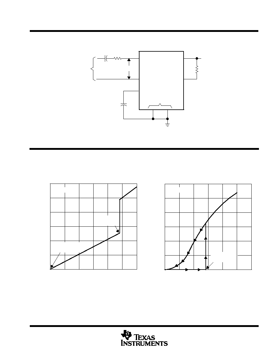
PARAMETER MEASUREMENT INFORMATION
AC
INPUT
AC
INPUT
5-V OUTPUT
INVERTING
OUTPUT
C FILTER
COMMON
1
8
6
3
7
4
2
TCM1520A
Output
10
µ
F,
50 V
2.2 k
VIrms = 40 V to 150 V
10 k
VID
0.47
µ
F,
350 V
Figure 1. Switching Test Circuit
TYPICAL CHARACTERISTICS
9
6
3
0
8
10
12
Capacitor
V
oltage ≠ V
12
15
CAPACITOR VOLTAGE (C FILTER)
vs
DIFFERENTIAL INPUT VOLTAGE
(AC INPUT, PINS 1 AND 8)
18
14
16
18
20
VID ≠ Differential Input Voltage ≠ V
6.8-V Zener Diode
Starts to Conduct
Comparator
Switch Fires
3
2
1
0
4
5
6
≠ Output V
oltage ≠ V
4
5
Capacitor Voltage ≠ V
OUTPUT VOLTAGE (5-V OUTPUT)
vs
CAPACITOR VOLTAGE (C FILTER)
6
7
8
9
10
V
O
TA = 25
∞
C
Comparator
Switch Fires
TA = 25
∞
C
Figure 2
Figure 3
TCM1520A
RING DETECTOR
SCTS005B ≠ OCTOBER 1984 ≠ REVISED DECEMBER 1990
5
POST OFFICE BOX 655303
∑
DALLAS, TEXAS 75265
POST OFFICE BOX 1443
∑
HOUSTON, TEXAS 77251≠1443
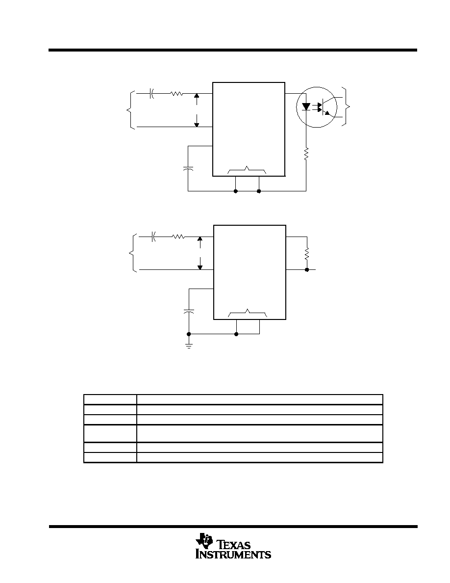
APPLICATION INFORMATION
AC
INPUT
AC
INPUT
5-V OUTPUT
C FILTER
COMMON
1
8
6
3
7
4
TCM1520A
C2 = 10
µ
F,
50 V
R1 = 2.2 k
VIrms = 40 V to 150 V,
15.3 Hz to 68 Hz
R2 = 2.2 k
VID
C1 = 0.47
µ
F,
350 V
TIL181
To Isolated
Output
Figure 4. Isolated Configuration
AC
INPUT
AC
INPUT
5-V OUTPUT
C FILTER
COMMON
1
8
6
3
7
4
TCM1520A
C2 = 10
µ
F,
50 V
R1 = 2.2 k
VIrms = 40 V to 150 V,
15.3 Hz to 68 Hz
10 k
VID
C1 = 0.47
µ
F,
350 V
INVERTING
OUTPUT
Output
2
Figure 5. Nonisolated Configuration
NOTE: See Table 1 for component functions.
TABLE 1. COMPONENT FUNCTIONS
COMPONENT
FUNCTION
R1
Limits current into SCR during high-voltage transients and aids in dial-pulse rejection.
R2
Limits current into light-emitting diode.
C1
Blocks dc-battery voltage in standby and aids in filtering dial pulses. Smaller values of C1
improve tapping immunity.
C2
Stores energy from the ring signal to power the 5-V regulator.
Optocoupler
Provides ground and transient isolation between the host system and the telephone line.