
TCM8002
DATA PROCESSOR FOR CELLULAR TELEPHONE
SLWS008C ≠ SEPTEMBER 1994 ≠ REVISED JUNE 1996
1
POST OFFICE BOX 655303
∑
DALLAS, TEXAS 75265
D
Single Chip for AMPS/TACS Data and SAT
Processing
D
3.3-V or 5-V Operation
D
Simple Serial Interface
D
User-Configurable Interrupt Structure
D
TX and RX Data Buffers
D
Programmable Timer
D
Independent Watchdog Timer
D
RX/TX Automatic Mute Functions
D
Arbitration Processing
D
20 Programmable Expansion I/O Ports
D
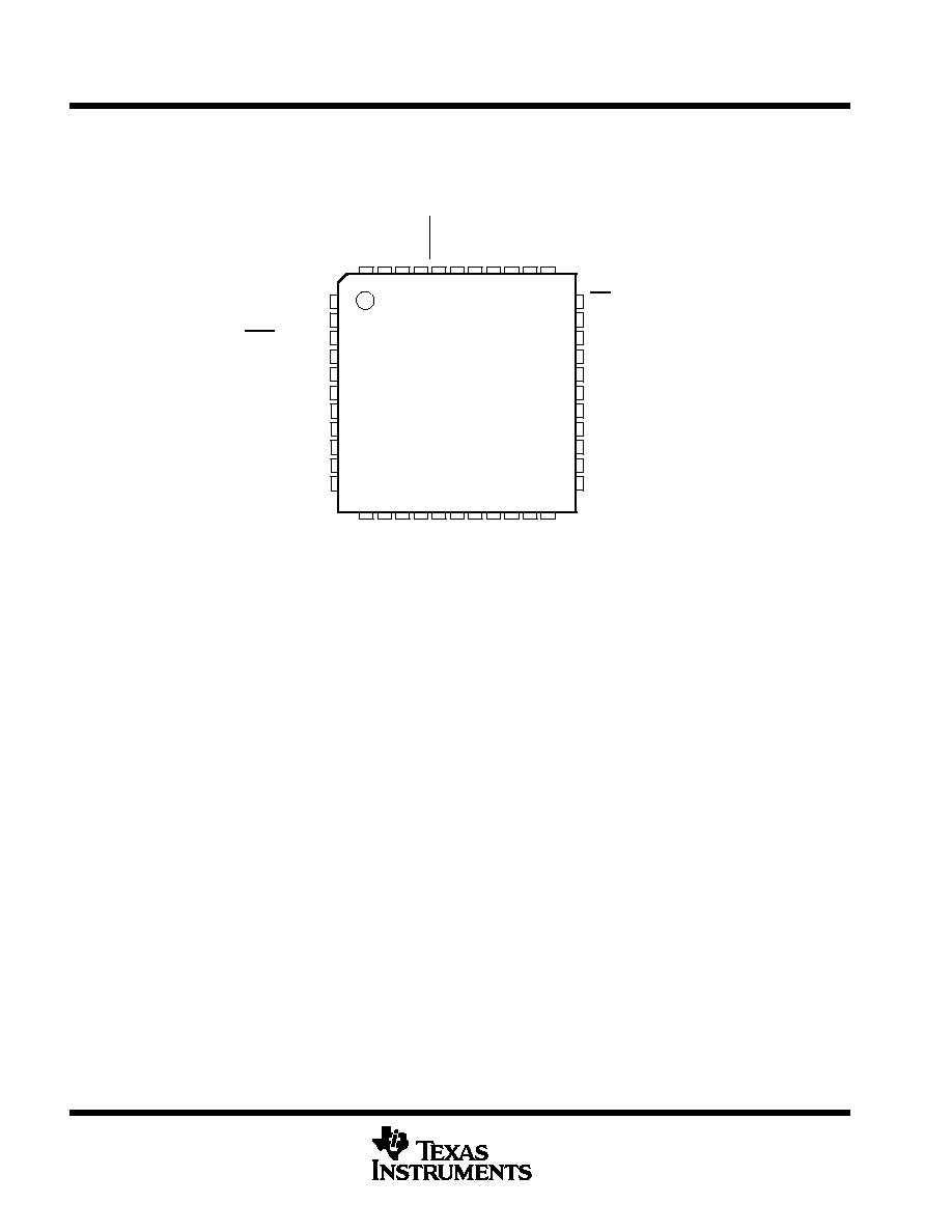
44-Pin Mini-QFP FR Package
description
The TCM8002 provides the data transceiving, data processing, and SAT (supervisory audio tone) functions for
the AMPS (advanced mobile phone service) and TACS (total access communications system) cellular
telephone standards. A highly integrated device, the TCM8002 includes a number of additional functions that
are helpful in the implementation of the typical cellular telephone. These extra functions include a watchdog
timer, which is normally external to the telephone microcontroller, and two 8-bit- and one 4-bit-wide
user-programmable general-purpose input/output ports. These can be used to provide port expansion for the
microcontroller. An 8-bit counter/timer for user-defined purposes is also included.
To facilitate the application of the TCM8002 and to minimize the number of connections, a single serial interface
to the microcontroller is used for controlling, receiving, and transmitting data. There is also a dedicated interface,
including a compatible clock signal, to the companion TCM8010 audio processor that performs most of the
audio processing required in a cellular telephone. Additional outputs are also provided for interfacing to other
audio processors.
The TCM8002 is built using a low-power CMOS process and operates with a 5-V or 3.3-V power supply. When
used in conjunction with the TCM8010, a unique and very compact low-power solution for AMPS/TACS
baseband processing in 5-V and 3-V systems is realized.
Please be aware that an important notice concerning availability, standard warranty, and use in critical applications of
Texas Instruments semiconductor products and disclaimers thereto appears at the end of this data sheet.
PRODUCTION DATA information is current as of publication date.
Products conform to specifications per the terms of Texas Instruments
standard warranty. Production processing does not necessarily include
testing of all parameters.
Copyright
©
1996, Texas Instruments Incorporated
TCM8002
DATA PROCESSOR FOR CELLULAR TELEPHONE
SLWS008C ≠ SEPTEMBER 1994 ≠ REVISED JUNE 1996
2
POST OFFICE BOX 655303
∑
DALLAS, TEXAS 75265
CS
RCCBUSY/PO4(4)
WDOUT
RFEN
PIO3(3)
PIO3(2)
PIO3(1)
PIO3(0)
PIO2(7)
PIO2(6)
PIO2(5)
33
32
31
30
29
28
27
26
25
24
23
12 13
1
2
3
4
5
6
7
8
9
10
11
HDATA/PO4(0)
CLKOUT/PO4(1)
HCS/PO4(2)
HCLK/PO4(3)
SATOUT
TXOUT
SATIN
RXIN
PIO1(0)
PIO1(1)
PIO1(2)
14 15 16 17
FR PACKAGE
(TOP VIEW)
INTRPT
DCLK
DA
T
AIN
DA
T
AOUT
43 42 41 40 39
44
38
T
AEN/PO4(7)
RAEN/PO4(6)
XT
AL2
XT
AL1
RESET
TMZERO/PO4(5)
PIO2(1)
PIO2(2)
PIO2(3)
PIO1(3)
PIO1(4)
PIO1(5)
PIO1(6)
PIO1(7)
PIO2(0)
36 35 34
37
18 19 20 21 22
PIO2(4)
V
DD
V
SS
TCM8002
DATA PROCESSOR FOR CELLULAR TELEPHONE
SLWS008C ≠ SEPTEMBER 1994 ≠ REVISED JUNE 1996
3
POST OFFICE BOX 655303
∑
DALLAS, TEXAS 75265
functional block diagram
HDATA/PO4(0)
RCCBUSY/
PO4(4)
Clock
Divider
Watchdog
Timer
From Microprocessor
Interface
TCM8010
Interface
SAT
Detector/
Regenerator
Data
Recovery
RX
Control
Majority
Voting
BCH
Decoder
RX
Buffer
Microprocessor
Interface
Interrupt
Circuit
Arbitration
Logic
TX
Encoder
TX
Buffer
Programmable I/O Extension
Counter/
Timer
XTAL1
XTAL2
RESET
9 ≠ 16
PIO1(0 ≠ 7)
18 ≠ 25
PIO2(0 ≠ 7)
26 ≠ 29
PIO3(0 ≠ 3)
HCS/PO4(2)
HCLK/PO4(3)
SATOUT
SATIN
RXIN
RAEN/PO4(6)
RFEN
TAEN/PO4(7)
TXOUT
WDOUT
DATAOUT
DATAIN
CS
DCLK
INTRPT
TMZERO/
PO4(5)
8
8
4
41
42
40
31
3
4
1
5
7
8
43
30
44
6
32
35
34
36
33
37
38
CLKOUT/PO4(1)
2
( ) = bit count
TCM8002
DATA PROCESSOR FOR CELLULAR TELEPHONE
SLWS008C ≠ SEPTEMBER 1994 ≠ REVISED JUNE 1996
4
POST OFFICE BOX 655303
∑
DALLAS, TEXAS 75265
Terminal Functions
TERMINAL
I/O
DESCRIPTION
NAME
NO.
I/O
DESCRIPTION
CLKOUT/PO4(1)
2
O
Clock output / programmable output #4, bit 1. A 2.56-MHz clock signal is output on this terminal or the
device can be set so that it is bit 1 of PO4.
CS
33
I
Chip select (active low). This is the chip select input from the microcontroller.
DATAIN
35
I
Data input. Serial data from the microcontroller is input on this terminal.
DATAOUT
34
O
Data output. This is the serial data output to the microcontroller (3-state).
DCLK
36
I
Data clock. This is the serial microcontroller interface clock input.
HCLK/PO4(3)
4
O
TCM8010 interface clock / programmable output #4, bit 3. A clock signal to the TCM8010 or bit 3 of
programmable output 4 is output on this terminal.
HDATA/PO4(0)
1
I/O
TCM8010 interface data line/programmable output #4, bit 0. This terminal is used for data to and from
the TCM8010, or is bit 3 of programmable output 4.
HCS/PO4(2)
3
O
TCM8010 interface chip select output (active-low) / programmable output #4, bit 2. This terminal
selects the TCM8010, or is bit 2 of programmable output 4.
INTRPT
37
O
Interrupt output. This is the interrupt line to the microprocessor.
PIO1(0 ≠ 7)
9 ≠ 16
I/O
Programmable I/O port #1, bits 0 ≠ 7. This 8-bit port can be configured as either inputs or outputs
(microcontroller port expansion).
PIO2(0 ≠ 7)
18 ≠ 25
I/O
Programmable I/O port #2, bits 0 ≠ 7. This 8-bit port can be configured as either inputs or outputs
(microcontroller port expansion).
PIO3(0 ≠ 3)
26 ≠ 29
I/O
Programmable I/O port #3, bits 0 ≠ 3. This 4-bit port can be configured as either inputs or outputs
(microcontroller port expansion).
RAEN/PO4(6)
43
O
Receive audio enable output/programmable output #4, bit 6. This terminal is used to enable the
receive audio section of the phone, or is bit 6 of programmable output 4 (open drain).
RCCBUSY/PO4(4)
32
O
RECC busy status/programmable output #4, bit 4. This terminal outputs the status result of the
majority vote of the three most recent busy/idle bits, or is bit 4 of programmable output 4.
RESET
40
I
Reset input, active low. A low applied to this terminal resets the TCM8002 and loads the default values
listed in the write map.
RFEN
30
O
RF enable. This terminal is used to enable the transmitter section of the phone (open drain).
RXIN
8
I
Baseband Manchester data input. Manchester-encoded data from control or voice channel is input
on this terminal.
SATIN
7
I
SAT input. Square-wave SAT data from the TCM8010 audio processor is input on this terminal.
SATOUT
5
O
Regenerated SAT output. Regenerated SAT data is output to the TCM8010 audio processor on this
terminal.
TAEN/PO4(7)
44
O
Transmit audio enable/programmable output #4, bit 7. The logic level on this terminal changes state
during RVC message or ST transmission, or is bit 7 of programmable output 4 (open drain).
TMZERO/PO4(5)
38
O
Timer zero/programmable output #4, bit 5. The logic level on this terminal changes state when the
counter/timer passes or reaches zero, or is bit 5 of programmable output 4.
TXOUT
6
O
Transmit data output. Encoded transmit data is output to the TMC8010 audio processor on this
terminal.
VDD
39
Positive supply voltage. Input is 3.3-V or 5-V.
VSS
17
Ground supply voltage.
WDOUT
31
O
Watchdog timer output. A logic-low pulse is output on this terminal when the watchdog timer times
out.
XTAL1
41
I
Crystal terminal 1/external clock source input. An external crystal is connected to this terminal for the
internal clock oscillator. An external clock signal can also be input on this terminal.
XTAL2
42
O
Crystal terminal 2. An external crystal is connected to this terminal for the internal clock oscillator.
All inputs feature Schmitt triggers. All of the PIO terminals also feature optional 10-
µ
A pullups.
( ) = bit count when in the terminal column

TCM8002
DATA PROCESSOR FOR CELLULAR TELEPHONE
SLWS008C ≠ SEPTEMBER 1994 ≠ REVISED JUNE 1996
5
POST OFFICE BOX 655303
∑
DALLAS, TEXAS 75265
detailed description
Data communication between the mobile station and the land station in AMPS and TACS systems is achieved
over forward and reverse control channels when a call is not in progress, or in short bursts over the forward and
reverse voice channels when a call is in progress. The TCM8002 device has a receive path that recovers data
from the FOCC (forward control-channel) and FVC (forward voice-channel) formats. The transmit path encodes
and formats data for the RECC (reverse control channel) and RVC (reverse voice channel).
For voice-channel communications, the received SAT is detected and regenerated for transmission.
Communication with the microcontroller/microprocessor in the telephone is through a serial interface. The
TCM8002 also provides interrupts to alert the processor to the occurrence of specific events. The receiver is
made up of the Data Recovery, Majority Voting, BCH (Bose-Chaudhuri-Hocquenghem) Decoder, RX Buffer,
Arbitration Logic, and RX Control blocks. The SAT Detector/Regenerator is used during FVC reception and RVC
transmission.
The transmit path consists of the TX Buffer and TX Encoder blocks. A serial microprocessor interface and the
interrupt logic are also provided. Four ancillary functions are included:
∑
TCM8010 interface
∑
Watchdog Timer
∑
Counter/Timer
∑
twenty programmable digital bidirectional I/O lines (eight of the output terminals can be reconfigured as
processor output ports)
clock divider
The clock signal for the TCM8002 is supplied in two ways:
∑
A crystal can be connected to XTAL1 and XTAL2.
∑
A clock signal from another source can be connected to XTAL1.
When a crystal is used, a resistor (typical value 1 M
) should be connected between XTAL1 and XTAL2 to
provide a bias for the oscillator. The crystal frequency must be 2.56 MHz, 5.12 MHz, 7.68 MHz, or 10.24 MHz.
If an external clock signal is connected, it must be at one of these crystal frequencies or one of two additional
frequencies: 15.36 MHz or 20.48 MHz.
The clock frequency defaults to 2.56 MHz when the TCM8002 is reset. The clock-divider circuit provides a
2.56-MHz clock for internal use and must be configured according to the selected crystal or external clock
frequency. Control word 2, bits 5 and 6, and control word 4, bit 1, are used to configure the clock divider. The
output from the clock-divider circuit is provided at CLKOUT and is always 2.56 MHz. This can be used to clock
the TCM8010 advanced audio processor.
The bit rate of the transmitted Manchester-encoded data, the signaling-tone frequency, and the accuracy of the
SAT measurement are all determined by the crystal or external clock. The AMPS and TACS system
requirements both specify a maximum transmitted bit frequency error of
±
100 ppm; therefore, over the
operating temperature range of the phone, the crystal or clock frequency error must be no more than
±
100 ppm.