TIBPAL16L8-10C, TIBPAL16R4-10C, TIBPAL16R6-10C, TIBPAL16R8-10C
TIBPAL16L8-12M, TIBPAL16R4-12M, TIBPAL16R6-12M, TIBPAL16R8-12M
HIGH-PERFORMANCE IMPACT-X
TM
PAL
Æ
CIRCUITS
SRPS017 ≠ D3023, MAY 1987 ≠ REVISED MARCH 1992
POST OFFICE BOX 655303
∑
DALLAS, TEXAS 75265
Copyright
©
1992, Texas Instruments Incorporated
1
PRODUCTION DATA information is current as of publication date.
Products conform to specifications per the terms of Texas Instruments
standard warranty. Production processing does not necessarily include
testing of all parameters.
∑
High-Performance Operation:
f
max
(w/o feedback)
TIBPAL16R '-10C Series . . . 62.5 MHz Min
TIBPAL16R' -12M Series . . . 56 MHz Min
f
max
(with feedback)
TIBPAL16R' -10C Series . . . 55.5 MHz Min
TIBPAL16R' -12M Series . . . 48 MHz Min
Propagation Delay
TIBPAL16L'-10C Series . . . 10 ns Max
TIBPAL16L'-12M Series . . . 12 ns Max
∑
Functionally Equivalent, but Faster than,
Existing 20-Pin PLDs
∑
Preload Capability on Output Registers
Simplifies Testing
∑
Power-Up Clear on Registered Devices (All
Register Outputs are Set Low, but Voltage
Levels at the Output Pins Go High)
∑
Package Options Include Both Plastic and
Ceramic Chip Carriers in Addition to Plastic
and Ceramic DIPs
∑
Security Fuse Prevents Duplication
∑
Dependable Texas Instruments Quality and
Reliability
DEVICE
I
INPUTS
3-STATE
O OUTPUTS
REGISTERED
Q OUTPUTS
I/O
PORT
S
PAL16L8
10
2
0
6
PAL16R4
8
0
4 (3-state buffers)
4
PAL16R6
8
0
6 (3-state buffers)
2
PAL16R8
8
0
8 (3-state buffers)
0
description
These programmable array logic devices feature high speed and functional equivalency when compared with
currently available devices. These IMPACT-X
TM
circuits combine the latest Advanced Low-Power Schottky
technology with proven titanium-tungsten fuses to provide reliable, high-performance substitutes for
conventional TTL logic. Their easy programmability allows for quick design of custom functions and typically
results in a more compact circuit board. In addition, chip carriers are available for futher reduction in board
space.
All of the register outputs are set to a low level during power up. Extra circuitry has been provided to allow loading
of each register asynchronously to either a high or low state. This feature simplifies testing because the registers
can be set to an initial state prior to executing the test sequence.
The TIBPAL16' C series is characterized from 0
∞
C to 75
∞
C. The TIBPAL16' M series is characterized for
operation over the full military temperature range of ≠55
∞
C to 125
∞
C.
These devices are covered by U.S. Patent 4,410,987.
IMPACT-X is a trademark of Texas Instruments Incorporated.
PAL is a registered trademark of Advanced Micro Devices Inc.
Pin assignments in operating mode
1
2
3
4
5
6
7
8
9
10
20
19
18
17
16
15
14
13
12
11
I
I
I
I
I
I
I
I
I
GND
VCC
O
I/O
I/O
I/O
I/O
I/O
I/O
O
I
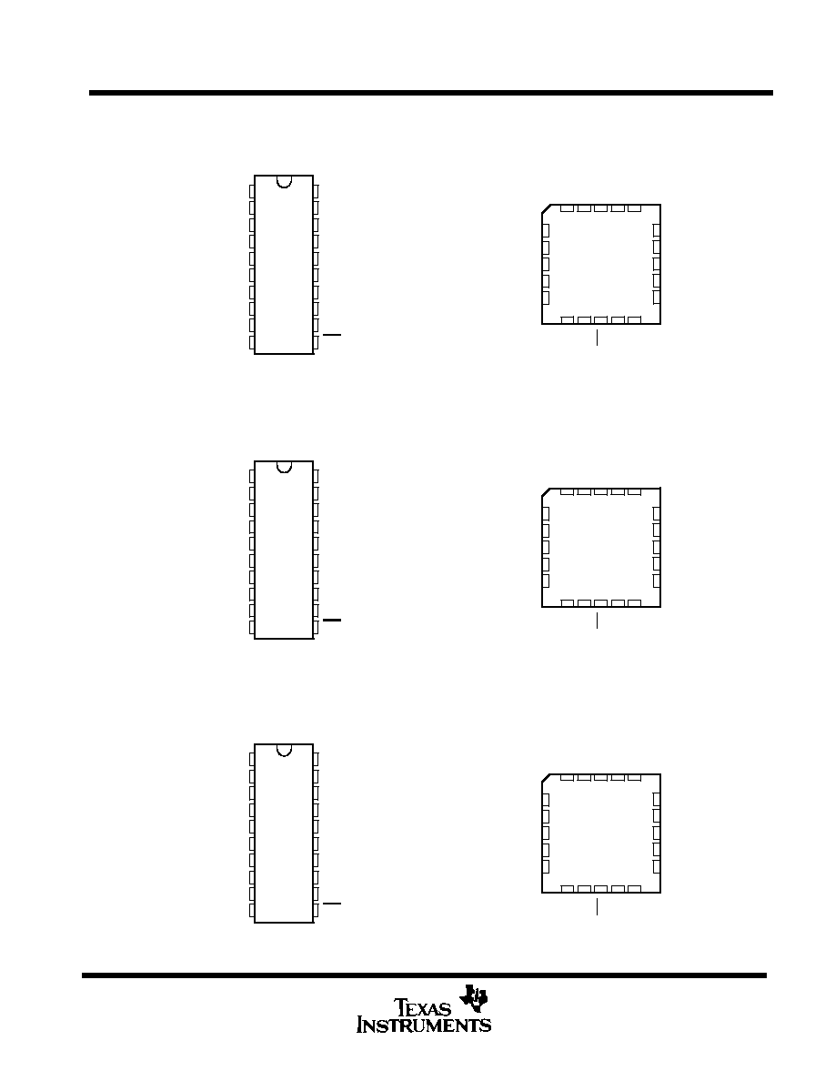
TIBPAL16L8'
C SUFFIX . . . J OR N PACKAGE
M SUFFIX . . . J PACKAGE
(TOP VIEW)
3
2
1 20 19
9 10 11 12 13
4
5
6
7
8
18
17
16
15
14
I/O
I/O
I/O
I/O
I/O
I
I
I
I
I
TIBPAL16L8'
C SUFFIX . . . FN PACKAGE
M SUFFIX . . . FK PACKAGE
(TOP VIEW)
I
I
I
O
I/O
O
I
GND
I
V
CC
TIBPAL16R4-10C, TIBPAL16R6-10C, TIBPAL16R8-10C
TIBPAL16R4-12M, TIBPAL16R6-12M, TIBPAL16R8-12M
HIGH-PERFORMANCE IMPACT-X
TM
PAL
Æ
CIRCUITS
SRPS017 ≠ D3023, MAY 1987 ≠ REVISED MARCH 1992
POST OFFICE BOX 655303
∑
DALLAS, TEXAS 75265
2
Pin assignments in operating mode
1
2
3
4
5
6
7
8
9
10
20
19
18
17
16
15
14
13
12
11
CLK
I
I
I
I
I
I
I
I
GND
VCC
I/O
I/O
Q
Q
Q
Q
I/O
I/O
OE
(TOP VIEW)
TIBPAL16R4'
C SUFFIX . . . J OR N PACKAGE
M SUFFIX . . . J PACKAGE
1
2
3
4
5
6
7
8
9
10
20
19
18
17
16
15
14
13
12
11
CLK
I
I
I
I
I
I
I
I
GND
VCC
I/O
Q
Q
Q
Q
Q
Q
I/O
OE
(TOP VIEW)
TIBPAL16R6'
C SUFFIX . . . J OR N PACKAGE
M SUFFIX . . . J PACKAGE
1
2
3
4
5
6
7
8
9
10
20
19
18
17
16
15
14
13
12
11
CLK
I
I
I
I
I
I
I
I
GND
VCC
Q
Q
Q
Q
Q
Q
Q
Q
OE
(TOP VIEW)
TIBPAL16R8'
C SUFFIX . . . J OR N PACKAGE
M SUFFIX . . . J PACKAGE
I
I
CLK
I/O
I/O
I/O
I
GND
V
CC
OE
3
2
1 20 19
9 10 11 12 13
4
5
6
7
8
18
17
16
15
14
I/O
Q
Q
Q
Q
I
I
I
I
I
(TOP VIEW)
TIBPAL16R4'
C SUFFIX . . . FN PACKAGE
M SUFFIX . . . FK PACKAGE
I
I
CLK
I/O
Q
I/O
I
GND
V
CC
3
2
1 20 19
9 10 11 12 13
4
5
6
7
8
18
17
16
15
14
Q
Q
Q
Q
Q
I
I
I
I
I
(TOP VIEW)
OE
TIBPAL16R6'
C SUFFIX . . . FN PACKAGE
M SUFFIX . . . FK PACKAGE
I
I
CLK
Q
Q
Q
I
GND
V
CC
OE
3
2
1 20 19
9 10 11 12 13
4
5
6
7
8
18
17
16
15
14
Q
Q
Q
Q
Q
I
I
I
I
I
(TOP VIEW)
TIBPAL16R8'
C SUFFIX . . . FN PACKAGE
M SUFFIX . . . FK PACKAGE
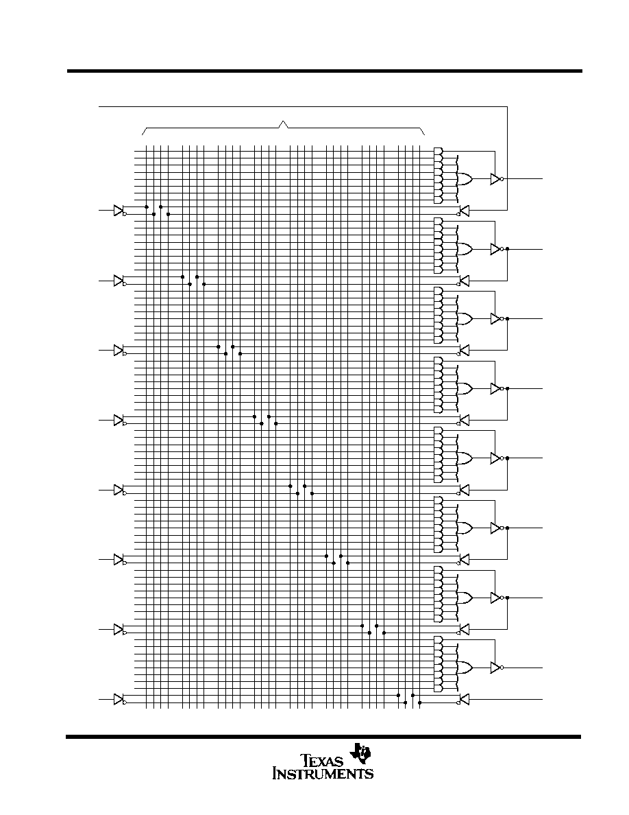
0
4
8
12
16
20
24
28
31
I
2
I
3
I
4
I
5
I
6
I
7
I
8
I
9
O
19
I/O
18
I/O
17
I/O
16
I/O
15
I/O
14
I/O
13
O
12
I
11
Increment
I
1
Fuse number = First fuse number + Increment
0
32
64
96
128
160
192
224
256
288
320
352
384
416
448
480
512
544
576
608
640
672
704
736
768
800
832
864
896
928
960
992
1024
1056
1088
1120
1152
1184
1216
1248
1280
1312
1344
1376
1408
1440
1472
1504
1536
1568
1600
1632
1664
1696
1728
1760
1792
1824
1856
1888
1920
1952
1984
2016
First
Fuse
Numbers
TIBPAL16L8-10C
TIBPAL16L8-12M
HIGH-PERFORMANCE IMPACT-X
TM
PAL
Æ
CIRCUITS
SRPS017 ≠ D3023, MAY 1987 ≠ REVISED MARCH 1992
POST OFFICE BOX 655303
∑
DALLAS, TEXAS 75265
5
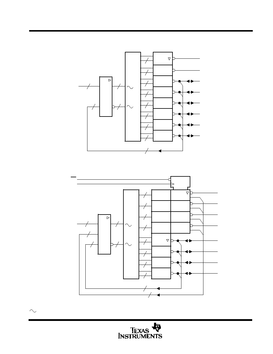
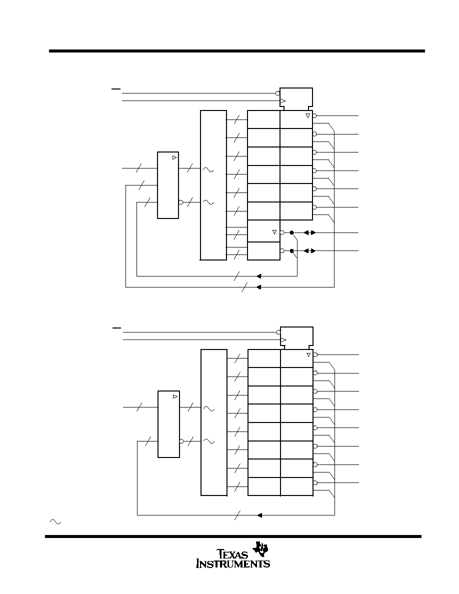
logic diagram (positive logic)