TL071, TL071A, TL071B, TL072
TL072A, TL072B, TL074, TL074A, TL074B
LOW NOISE JFET INPUT OPERATIONAL AMPLIFIERS
SLOS080J - SEPTEMBER 1978 - REVISED MARCH 2005
1
POST OFFICE BOX 655303
∑
DALLAS, TEXAS 75265
D
Low Power Consumption
D
Wide Common-Mode and Differential
Voltage Ranges
D
Low Input Bias and Offset Currents
D
Output Short-Circuit Protection
D
Low Total Harmonic Distortion
. . . 0.003% Typ
D
Low Noise
V
n
= 18 nV/
Hz Typ at f = 1 kHz
D
High Input Impedance . . . JFET Input Stage
D
Internal Frequency Compensation
D
Latch-Up-Free Operation
D
High Slew Rate . . . 13 V/
µ
s Typ
D
Common-Mode Input Voltage Range
Includes V
CC+
description/ordering information
The JFET-input operational amplifiers in the TL07x series are similar to the TL08x series, with low input bias
and offset currents and fast slew rate. The low harmonic distortion and low noise make the TL07x series ideally
suited for high-fidelity and audio preamplifier applications. Each amplifier features JFET inputs (for high input
impedance) coupled with bipolar output stages integrated on a single monolithic chip.
The C-suffix devices are characterized for operation from 0
∞
C to 70
∞
C. The I-suffix devices are characterized
for operation from -40
∞
C to 85
∞
C. The M-suffix devices are characterized for operation over the full military
temperature range of -55
∞
C to 125
∞
C.
Please be aware that an important notice concerning availability, standard warranty, and use in critical applications of
Texas Instruments semiconductor products and disclaimers thereto appears at the end of this data sheet.
Copyright
2005, Texas Instruments Incorporated
PRODUCTION DATA information is current as of publication date.
Products conform to specifications per the terms of Texas Instruments
standard warranty. Production processing does not necessarily include
testing of all parameters.
On products compliant to MIL PRF 38535, all parameters are tested
unless otherwise noted. On all other products, production
processing does not necessarily include testing of all parameters.

TL071, TL071A, TL071B, TL072
TL072A, TL072B, TL074, TL074A, TL074B
LOW NOISE JFET INPUT OPERATIONAL AMPLIFIERS
SLOS080J - SEPTEMBER 1978 - REVISED MARCH 2005
2
POST OFFICE BOX 655303
∑
DALLAS, TEXAS 75265
description/ordering information (continued)
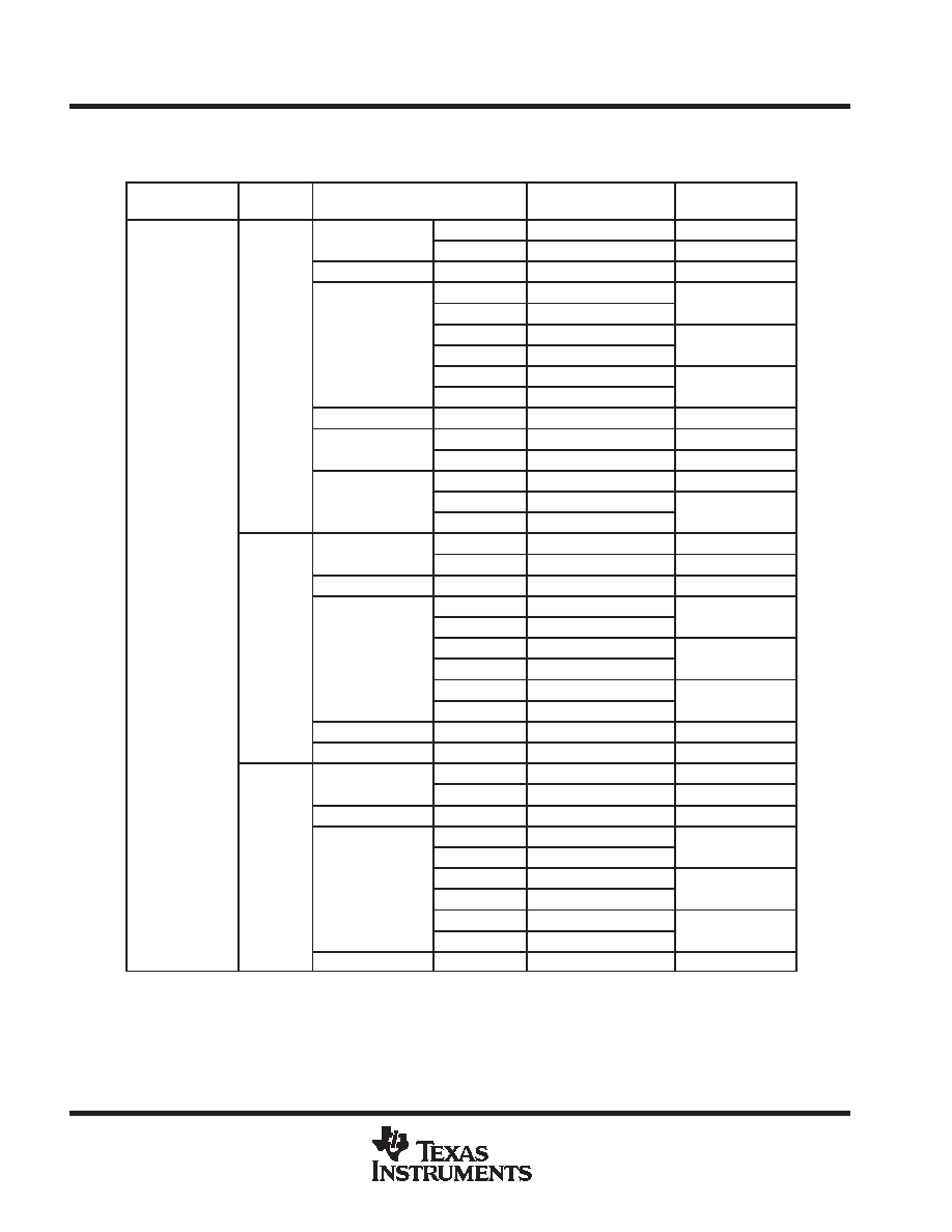
ORDERING INFORMATION
TA
VIOmax
AT 25
∞
C
PACKAGE
ORDERABLE
PART NUMBER
TOP-SIDE
MARKING
PDIP (P)
Tube of 50
TL071CP
TL071CP
PDIP (P)
Tube of 50
TL072CP
TL072CP
PDIP (N)
Tube of 25
TL074CN
TL074CN
Tube of 75
TL071CD
TL071C
Reel of 2500
TL071CDR
TL071C
SOIC (D)
Tube of 75
TL072CD
TL072C
SOIC (D)
Reel of 2500
TL072CDR
TL072C
10 mV
Tube of 50
TL074CD
TL074C
10 mV
Reel of 2500
TL074CDR
TL074C
SOP (NS)
Reel of 2000
TL074CNSR
TL074
SOP (PS)
Reel of 2000
TL071CPSR
TL071
SOP (PS)
Reel of 2000
TL072CPSR
T072
Reel of 2000
TL072CPWR
T072
TSSOP (PW)
Tube of 90
TL074CPW
T074
TSSOP (PW)
Reel of 2000
TL074CPWR
T074
PDIP (P)
Tube of 50
TL071ACP
TL071ACP
PDIP (P)
Tube of 50
TL072ACP
TL072ACP
0
∞
C to 70
∞
C
PDIP (N)
Tube of 25
TL074ACN
TL074ACN
0
∞
C to 70
∞
C
Tube of 75
TL071ACD
071AC
Reel of 2500
TL071ACDR
071AC
6 mV
SOIC (D)
Tube of 75
TL072ACD
072AC
6 mV
SOIC (D)
Reel of 2500
TL072ACDR
072AC
Tube of 50
TL074ACD
TL074AC
Reel of 2500
TL074ACDR
TL074AC
SOP (PS)
Reel of 2000
TL072ACPSR
T072A
SOP (NS)
Reel of 2000
TL074ACNSR
TL074A
PDIP (P)
Tube of 50
TL071BCP
TL071BCP
PDIP (P)
Tube of 50
TL072BCP
TL072BCP
PDIP (N)
Tube of 25
TL074BCN
TL074BCN
Tube of 75
TL071BCD
071BC
3 mV
Reel of 2500
TL071BCDR
071BC
3 mV
SOIC (D)
Tube of 75
TL072BCD
072BC
SOIC (D)
Reel of 2500
TL072BCDR
072BC
Tube of 50
TL074BCD
TL074BC
Reel of 2500
TL074BCDR
TL074BC
SOP (NS)
Reel of 2000
TL074BCNSR
TL074B
Package drawings, standard packing quantities, thermal data, symbolization, and PCB design guidelines are available at
www.ti.com/sc/package.

TL071, TL071A, TL071B, TL072
TL072A, TL072B, TL074, TL074A, TL074B
LOW NOISE JFET INPUT OPERATIONAL AMPLIFIERS
SLOS080J - SEPTEMBER 1978 - REVISED MARCH 2005
3
POST OFFICE BOX 655303
∑
DALLAS, TEXAS 75265
description/ordering information (continued)
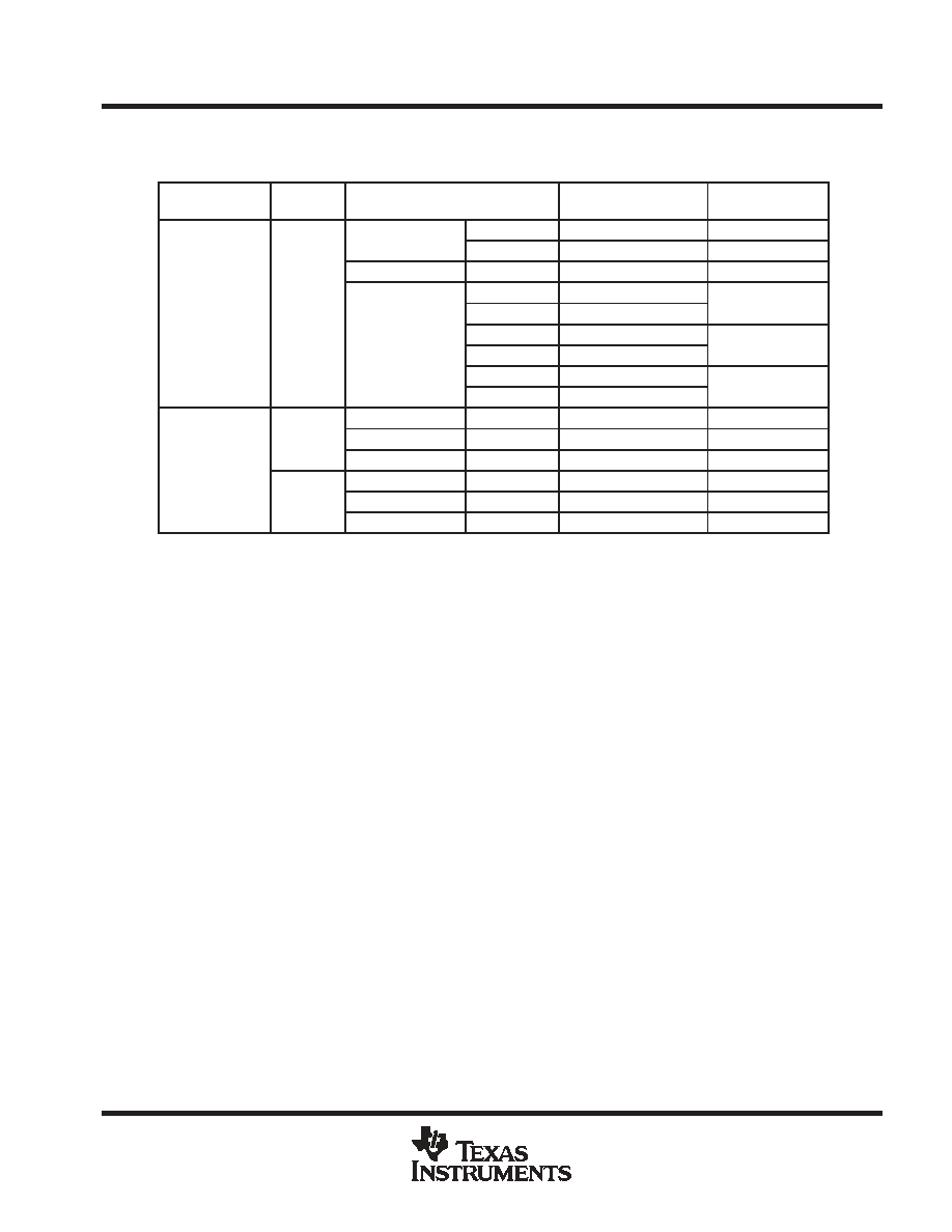
ORDERING INFORMATION
TA
VIOmax
AT 25
∞
C
PACKAGE
ORDERABLE
PART NUMBER
TOP-SIDE
MARKING
PDIP (P)
Tube of 50
TL071IP
TL071IP
PDIP (P)
Tube of 50
TL072IP
TL072IP
PDIP (N)
Tube of 25
TL074IN
TL074IN
Tube of 75
TL071ID
TL071I
-40
∞
C to 85
∞
C
6 mV
Reel of 2500
TL071IDR
TL071I
-40 C to 85 C
6 mV
SOIC (D)
Tube of 75
TL072ID
TL072I
SOIC (D)
Reel of 2500
TL072IDR
TL072I
Tube of 50
TL074ID
TL074I
Reel of 2500
TL074IDR
TL074I
CDIP (JG)
Tube of 50
TL072MJGB
TL072MJGB
6 mV
CFP (U)
Tube of 150
TL072MUB
TL072MUB
-55
∞
C to 125
∞
C
6 mV
LCCC (FK)
Tube of 55
TL072MFKB
TL072MFKB
-55
∞
C to 125
∞
C
CDIP (J)
Tube of 25
TL074MJB
TL074MJB
9 mV
CFP (W)
Tube of 25
TL074MWB
TL074MWB
9 mV
LCCC (FK)
Tube of 55
TL074MFKB
TL074MFKB
Package drawings, standard packing quantities, thermal data, symbolization, and PCB design guidelines are available at
www.ti.com/sc/package.

TL071, TL071A, TL071B, TL072
TL072A, TL072B, TL074, TL074A, TL074B
LOW NOISE JFET INPUT OPERATIONAL AMPLIFIERS
SLOS080J - SEPTEMBER 1978 - REVISED MARCH 2005
4
POST OFFICE BOX 655303
∑
DALLAS, TEXAS 75265
NC
2OUT
NC
2IN-
NC
1IN+
NC
V
CC+
NC
2IN+
NC
V
CC+
NC
OUT
NC
3
2
1 20 19
9 10 11 12 13
4
5
6
7
8
18
17
16
15
14
NC
1IN-
NC
1IN+
NC
(TOP VIEW)
NC
1OUT
NC
NC
NC
NC
NC
2IN+
CC-
V
CC+
V
1
2
3
4
5
6
7
14
13
12
11
10
9
8
1OUT
1IN-
1IN+
V
CC+
2IN+
2IN-
2OUT
4OUT
4IN-
4IN+
V
CC-
3IN+
3IN-
3OUT
TL074A, TL074B
D, J, N, NS, OR PW PACKAGE
TL074 . . . D, J, N, NS, PW,
OR W PACKAGE
(TOP VIEW)
NC - No internal connection
3
2
1 20 19
9 10 11 12 13
4
5
6
7
8
18
17
16
15
14
NC
IN-
NC
IN+
NC
TL071
FK PACKAGE
(TOP VIEW)
NC
OFFSET
N1
NC
NC
NC
NC
NC
OFFSET
N2
NC
CC-
V
TL072
FK PACKAGE
3
2
1 20 19
9 10 11 12 13
4
5
6
7
8
18
17
16
15
14
4IN+
NC
V
CC-
NC
3IN+
TL074
FK PACKAGE
(TOP VIEW)
1IN-
1OUT
NC
3IN-
4IN-
2IN-
NC
3OUT
4OUT
2OUT
1
2
3
4
8
7
6
5
OFFSET N1
IN-
IN+
V
CC-
NC
V
CC+
OUT
OFFSET N2
TL071, TL071A, TL071B
D, P, OR PS PACKAGE
(TOP VIEW)
1
2
3
4
8
7
6
5
1OUT
1IN-
1IN+
V
CC-
V
CC+
2OUT
2IN-
2IN+
TL072, TL072A, TL072B
D, JG, P, PS, OR PW PACKAGE
(TOP VIEW)
TL072
U PACKAGE
(TOP VIEW)
1
2
3
4
5
10
9
8
7
6
NC
1OUT
1IN-
1IN+
V
CC-
NC
V
CC+
2OUT
2IN-
2IN+
symbols
+
-
+
-
IN+
IN-
OUT
IN+
IN-
OUT
TL072 (each amplifier)
TL074 (each amplifier)
TL071
OFFSET N1
OFFSET N2

TL071, TL071A, TL071B, TL072
TL072A, TL072B, TL074, TL074A, TL074B
LOW NOISE JFET INPUT OPERATIONAL AMPLIFIERS
SLOS080J - SEPTEMBER 1978 - REVISED MARCH 2005
5
POST OFFICE BOX 655303
∑
DALLAS, TEXAS 75265
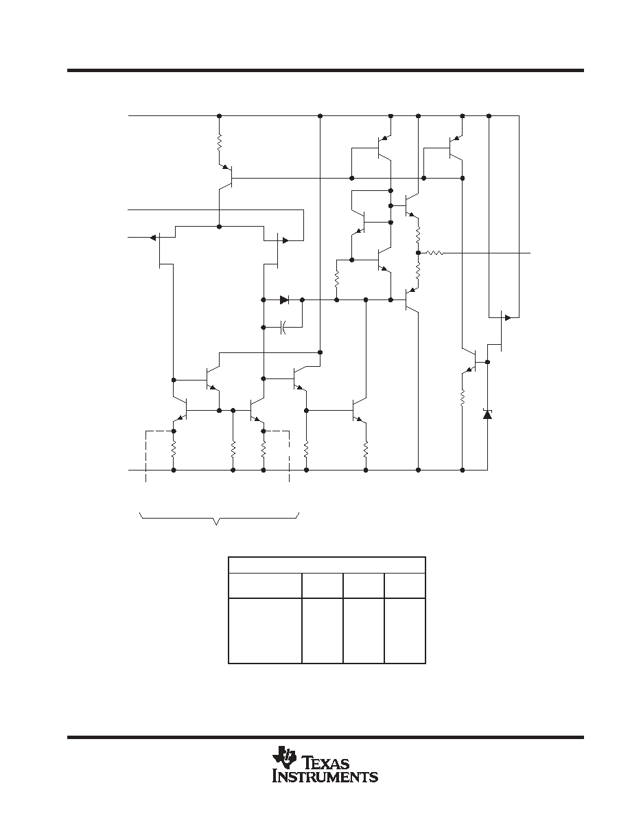
schematic (each amplifier)
C1
VCC+
IN+
VCC-
1080
ŒŒŒ
1080
IN-
TL071 Only
64
128
64
All component values shown are nominal.
¡¡¡¡¡
¡¡¡¡¡
OFFSET
N1
¡¡¡
¡¡¡
OFFSET
N2
OUT
18 pF
COMPONENT COUNT
COMPONENT
TYPE
TL071
TL072
TL074
Resistors
11
22
44
Resistors
Transistors
11
14
22
28
44
56
Transistors
JFET
14
2
28
4
56
6
JFET
Diodes
2
1
4
2
6
4
Diodes
Capacitors
epi-FET
1
1
1
2
2
2
4
4
4
Capacitors
epi-FET
1
1
2
2
4
4
Includes bias and trim circuitry
