 | –≠–ª–µ–∫—Ç—Ä–æ–Ω–Ω—ã–π –∫–æ–º–ø–æ–Ω–µ–Ω—Ç: TL598MJB | –°–∫–∞—á–∞—Ç—å:  PDF PDF  ZIP ZIP |

TL598
PULSE WIDTH MODULATION CONTROL CIRCUITS
SLVS053D - FEBRUARY 1988 - REVISED NOVEMBER 2003
1
POST OFFICE BOX 655303
∑
DALLAS, TEXAS 75265
D
Complete PWM Power-Control Function
D
Totem-Pole Outputs for 200-mA Sink or
Source Current
D
Output Control Selects Parallel or
Push-Pull Operation
D
Internal Circuitry Prohibits Double Pulse at
Either Output
D
Variable Dead-Time Provides Control Over
Total Range
D
Internal Regulator Provides a Stable 5-V
Reference Supply, Trimmed to 1%
Tolerance
D
On-Board Output Current-Limiting
Protection
D
Undervoltage Lockout for Low-V
CC
Conditions
D
Separate Power and Signal Grounds
description/ordering information
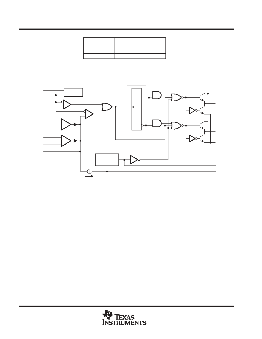
The TL598 incorporates all the functions required in the construction of pulse-width-modulated (PWM)
controlled systems on a single chip. Designed primarily for power-supply control, the TL598 provides the
systems engineer with the flexibility to tailor the power-supply control circuits to a specific application.
The TL598 contains two error amplifiers, an internal oscillator (externally adjustable), a dead-time control (DTC)
comparator, a pulse-steering flip-flop, a 5-V precision reference, undervoltage lockout control, and output
control circuits. Two totem-pole outputs provide exceptional rise- and fall-time performance for power FET
control. The outputs share a common source supply and common power ground terminals, which allow system
designers to eliminate errors caused by high current-induced voltage drops and common-mode noise.
The error amplifier has a common-mode voltage range of 0 V to V
CC
- 2 V. The DTC comparator has a fixed
offset that prevents overlap of the outputs during push-pull operation. A synchronous multiple supply operation
can be achieved by connecting RT to the reference output and providing a sawtooth input to CT.
The TL598 device provides an output control function to select either push-pull or parallel operation. Circuit
architecture prevents either output from being pulsed twice during push-pull operation. The output frequency
for push-pull applications is one-half the oscillator frequency f
O
+
1
2 RT CT
. For single-ended applications:
f
O
+
1
RT CT
.
ORDERING INFORMATION
TA
PACKAGE
ORDERABLE
PART NUMBER
TOP-SIDE
MARKING
PDIP (N)
Tube of 25
TL598CN
TL598CN
0
∞
C to 70
∞
C
SOIC (D)
Tube of 40
TL598CD
TL598C
0 C to 70 C
SOIC (D)
Reel of 2500
TL598CDR
TL598C
Package drawings, standard packing quantities, thermal data, symbolization, and PCB design guidelines are
available at www.ti.com/sc/package.
Copyright
2003, Texas Instruments Incorporated
PRODUCTION DATA information is current as of publication date.
Products conform to specifications per the terms of Texas Instruments
standard warranty. Production processing does not necessarily include
testing of all parameters.
Please be aware that an important notice concerning availability, standard warranty, and use in critical applications of
Texas Instruments semiconductor products and disclaimers thereto appears at the end of this data sheet.
1
2
3
4
5
6
7
8
16
15
14
13
12
11
10
9
1IN+
1IN-
FEEDBACK
DTC
CT
RT
SIGNAL GND
OUT1
2IN+
2IN-
REF
OUTPUT CTRL
VCC
VC
POWER GND
OUT2
D OR N PACKAGE
(TOP VIEW)
ERROR
AMP 1
ERROR
AMP 2
TL598
PULSE WIDTH MODULATION CONTROL CIRCUITS
SLVS053D - FEBRUARY 1988 - REVISED NOVEMBER 2003
2
POST OFFICE BOX 655303
∑
DALLAS, TEXAS 75265
FUNCTION TABLE
INPUT/OUTPUT
CTRL
OUTPUT FUNCTION
VI = GND
Single-ended or parallel output
VI = REF
Normal push-pull operation
functional block diagram
GND
SIGNAL
REF
VCC
Reference
Regulator
Undervoltage
Lockout Control
2
GND
POWER
OUT2
OUT1
VC
Pulse-Steering
Flip-Flop
C1
1D
FEEDBACK
-
+
1IN+
DTC
CT
RT
PWM
Comparator
Error Amplifier
1
+
-
Error Amplifier
0.1 V
DTC
Comparator
Oscillator
OUTPUT CTRL
(see Function Table)
6
5
4
1
2
16
15
3
13
11
8
9
10
12
14
7
1IN-
2IN+
2IN-
0.7 mA
absolute maximum ratings over operating free-air temperature range (unless otherwise noted)
Supply voltage, V
CC
(see Note 1)
41 V
. . . . . . . . . . . . . . . . . . . . . . . . . . . . . . . . . . . . . . . . . . . . . . . . . . . . . . . . . . . .
Amplifier input voltage, V
I
V
CC
+ 0.3 V
. . . . . . . . . . . . . . . . . . . . . . . . . . . . . . . . . . . . . . . . . . . . . . . . . . . . . . . . . . . .
Collector voltage
41 V
. . . . . . . . . . . . . . . . . . . . . . . . . . . . . . . . . . . . . . . . . . . . . . . . . . . . . . . . . . . . . . . . . . . . . . . . . . .
Output current (each output), sink or source, I
O
250
mA
. . . . . . . . . . . . . . . . . . . . . . . . . . . . . . . . . . . . . . . . . . . . .
Package thermal impedance,
JA
(see Notes 2 and 3): D package
73
∞
C/W
. . . . . . . . . . . . . . . . . . . . . . . . . . . .
N package
67
∞
C/W
. . . . . . . . . . . . . . . . . . . . . . . . . . . . .
Operating virtual junction temperature, T
J
150
∞
C
. . . . . . . . . . . . . . . . . . . . . . . . . . . . . . . . . . . . . . . . . . . . . . . . . . .
Storage temperature range, T
stg
-65
∞
C to 150
∞
C
. . . . . . . . . . . . . . . . . . . . . . . . . . . . . . . . . . . . . . . . . . . . . . . . . . .
Stresses beyond those listed under "absolute maximum ratings" may cause permanent damage to the device. These are stress ratings only, and
functional operation of the device at these or any other conditions beyond those indicated under "recommended operating conditions" is not
implied. Exposure to absolute-maximum-rated conditions for extended periods may affect device reliability.
NOTES:
1. All voltage values, except differential voltages, are with respect to the signal ground terminal.
2. Maximum power dissipation is a function of TJ(max),
JA, and TA. The maximum allowable power dissipation at any allowable
ambient temperature is PD = (TJ(max) - TA)/
JA. Operating at the absolute maximum TJ of 150
∞
C can impact reliability.
3. The package thermal impedance is calculated in accordance with JESD 51-7.

TL598
PULSE WIDTH MODULATION CONTROL CIRCUITS
SLVS053D - FEBRUARY 1988 - REVISED NOVEMBER 2003
3
POST OFFICE BOX 655303
∑
DALLAS, TEXAS 75265
recommended operating conditions
MIN
MAX
UNIT
VCC
Supply voltage
7
40
V
VI
Amplifier input voltage
0
VCC-2
V
IO
Collector voltage
40
V
IIL
Output current (each output), sink or source
200
mA
Current into feedback terminal
0.3
mA
CT
Timing capacitor
0.00047
10
µ
F
RT
Timing resistor
1.8
500
k
fosc
Oscillator frequency
1
300
kHz
TA
Operating free-air temperature
0
70
∞
C
electrical characteristics over recommended operating free-air temperature range, V
CC
= 15 V
(unless otherwise noted)
reference section (see Note 4)
PARAMETER
TEST CONDITIONS
MIN
TYP
MAX
UNIT
Output voltage (REF)
IO = 1 mA
TA = 25
∞
C
4.95
5
5.05
V
Output voltage (REF)
IO = 1 mA
TA = full range
4.9
5.1
V
Input regulation
VCC = 7 V to 40 V
TA = 25
∞
C
2
25
mV
Output regulation
IO = 1 mA to 10 mA
TA = 25
∞
C
1
15
mV
Output regulation
IO = 1 mA to 10 mA
TA = full range
50
mV
Output voltage change with temperature
TA = MIN to MAX
2
10
mV/V
Short-circuit output currentß
REF = 0 V
-10
-48
mA
Full range is 0
∞
C to 70
∞
C.
All typical values, except for parameter changes with temperature, are at TA = 25
∞
C.
ß Duration of the short circuit should not exceed one second.
NOTE 4: Pulse-testing techniques that maintain the junction temperature as close to the ambient temperature as possible must be used.
oscillator section, C
T
= 0.001
µ
F, R
T
= 12 k
(see Figure 1) (see Note 4)
PARAMETER
TEST CONDITIONS
MIN
TYP
MAX
UNIT
Frequency
100
kHz
Standard deviation of frequency∂
All values of VCC, CT, RT, TA constant
100
Hz/kHz
Frequency change with voltage
VCC = 7 V to 40 V,
TA = 25
∞
C
1
10
Hz/kHz
Frequency change with temperature#
TA = full range
70
120
Hz/kHz
Frequency change with temperature#
TA = full range,
CT = 0.01
µ
F
50
80
Hz/kHz
Full range is 0
∞
C to 70
∞
C.
All typical values, except for parameter changes with temperature, are at TA = 25
∞
C.
∂ Standard deviation is a measure of the statistical distribution about the mean, as derived from the formula:
# Effects of temperature on external RT and CT are not taken into account.
NOTE 4. Pulse-testing techniques that maintain the junction temperature as close to the ambient temperature as possible must be used.
s +
N
n
+
1
(xn
*
X)2
N
*
1

TL598
PULSE WIDTH MODULATION CONTROL CIRCUITS
SLVS053D - FEBRUARY 1988 - REVISED NOVEMBER 2003
4
POST OFFICE BOX 655303
∑
DALLAS, TEXAS 75265
electrical characteristics over recommended operating free-air temperature range, V
CC
= 15 V
(unless otherwise noted) (continued)
error amplifier section (see Note 4)
PARAMETER
TEST CONDITIONS
MIN
TYP
MAX
UNIT
Input offset voltage
FEEDBACK = 2.5 V
2
10
mV
Input offset current
FEEDBACK = 2.5 V
25
250
nA
Input bias current
FEEDBACK = 2.5 V
0.2
1
µ
A
Common-mode input voltage range
VCC = 7 V to 40 V
0 to
VCC-2
V
Open-loop voltage amplification
VO (FEEDBACK) = 3 V, VO (FEEDBACK) = 0.5 V to 3.5 V
70
95
dB
Unity-gain bandwidth
800
kHz
Common-mode rejection ratio
VCC = 40 V,
VIC = 6.5 V,
TA = 25
∞
C
65
80
dB
Output sink current (FEEDBACK)
FEEDBACK = 0.5 V
0.3
0.7
mA
Output source current (FEEDBACK)
FEEDBACK = 3.5 V
-2
mA
Phase margin at unity gain
FEEDBACK = 0.5 V to 3.5 V,
RL = 2 k
65
∞
Supply-voltage rejection ratio
FEEDBACK = 2.5 V,
VCC = 33 V,
RL = 2 k
100
dB
All typical values, except for parameter changes with temperature, are at TA = 25
∞
C.
NOTE 4. Pulse-testing techniques that maintain the junction temperature as close to the ambient temperature as possible must be used.
electrical characteristics over recommended operating free-air temperature range, V
CC
= 15 V
(unless otherwise noted)
undervoltage lockout section (see Note 4)
PARAMETER
TEST CONDITIONS
MIN
MAX
UNIT
Threshold voltage
TA = 25
∞
C
4
6
V
Threshold voltage
TA = full range
3.5
6.9
V
Hysteresisß
TA = 25
∞
C
100
mV
Hysteresisß
TA = full range
50
mV
Full range is 0
∞
C to 70
∞
C.
ß Hysteresis is the difference between the positive-going input threshold voltage and the negative-going input threshold voltage.
NOTE 4. Pulse-testing techniques must be used that maintain the junction temperature as close to the ambient temperature as possible.
output section (see Note 4)
PARAMETER
TEST CONDITIONS
MIN
MAX
UNIT
High-level output voltage
VCC = 15 V,
IO = -200 mA
12
V
High-level output voltage
VCC = 15 V,
VC = 15 V
IO = -20 mA
13
V
Low-level output voltage
VCC = 15 V,
IO = 200 mA
2
V
Low-level output voltage
VCC = 15 V,
VC = 15 V
IO = 20 mA
0.4
V
Output-control input current
VI = Vref
3.5
mA
Output-control input current
VI = Vref
VI = 0.4 V
100
µ
A
NOTE 4. Pulse-testing techniques must be used that maintain the junction temperature as close to the ambient temperature as possible.

TL598
PULSE WIDTH MODULATION CONTROL CIRCUITS
SLVS053D - FEBRUARY 1988 - REVISED NOVEMBER 2003
5
POST OFFICE BOX 655303
∑
DALLAS, TEXAS 75265
electrical characteristics over recommended operating free-air temperature range, V
CC
= 15 V
(unless otherwise noted) (continued)
dead-time control section (see Figure 1) (see Note 4)
PARAMETER
TEST CONDITIONS
MIN
TYP
MAX
UNIT
Input bias current (DTC)
VI = 0 to 5.25 V
-2
-10
µ
A
Maximum duty cycle, each output
DTC = 0 V
0.45
Input threshold voltage (DTC)
Zero duty cycle
3
3.3
V
Input threshold voltage (DTC)
Maximum duty cycle
0
V
All typical values, except for parameter changes with temperature, are at TA = 25
∞
C.
NOTE 4. Pulse-testing techniques must be used that maintain the junction temperature as close to the ambient temperature as possible.
pwm comparator section (see Note 4)
PARAMETER
TEST CONDITIONS
MIN
TYP
MAX
UNIT
Input threshold voltage (FEEDBACK)
DTC = 0 V
3.75
4.5
V
Input sink current (FEEDBACK)
V(FEEDBACK) = 0.5 V
0.3
0.7
mA
All typical values, except for parameter changes with temperature, are at TA = 25
∞
C.
NOTE Pulse-testing techniques must be used that maintain the junction temperature as close to the ambient temperature as possible.
total device (see Figure 1) (see Note 4)
PARAMETER
TEST CONDITIONS
MIN
TYP
MAX
UNIT
Standby supply current
RT = Vref,
All other inputs and outputs open
VCC = 15 V
15
21
mA
Standby supply current
RT = Vref,
All other inputs and outputs open
VCC = 40 V
20
26
mA
Average supply current
DTC = 2 V
15
mA
All typical values, except for parameter changes with temperature, are at TA = 25
∞
C.
NOTE 4. Pulse-testing techniques must be used that maintain the junction temperature as close to the ambient temperature as possible.
switching characteristics, T
A
= 25
∞
C
(see Note 4)
PARAMETER
TEST CONDITIONS
MIN
TYP
MAX
UNIT
Output-voltage rise time
CL = 1500 pF,
VC = 15 V,
VCC = 15 V,
See Figure 2
60
150
ns
Output-voltage fall time
CL = 1500 pF,
VC = 15 V,
VCC = 15 V,
See Figure 2
35
75
ns
NOTE 4. Pulse-testing techniques must be used that maintain the junction temperature as close to the ambient temperature as possible.

TL598
PULSE WIDTH MODULATION CONTROL CIRCUITS
SLVS053D - FEBRUARY 1988 - REVISED NOVEMBER 2003
6
POST OFFICE BOX 655303
∑
DALLAS, TEXAS 75265
PARAMETER MEASUREMENT INFORMATION
MAIN DEVICE TEST CIRCUIT
ERROR-AMPLIFIER TEST CIRCUIT
FEEDBACK
REF
-
+
VI
+
-
OUTPUT CONFIGURATION
VC
Output
POWER GND
OUTPUT 2
OUTPUT 1
15 V
50 k
15 V
POWER GND
OUT2
OUT1
VC
OUTPUT CTRL
REF
Inputs
Test
SIGNAL GND
RT
CT
DTC
FEEDBACK
IN-
IN+
VCC
IN-
IN+
12 k
0.001
µ
F
1
2
3
4
5
6
7
16
15
14
13
11
8
9
10
12
ERROR
AMP 1
ERROR
AMP 2
Figure 1. Test Circuits
OUTPUT CONFIGURATION
VC
Output
POWER GND
CL = 1500 pF
90%
10%
tr
tf
10%
90%
0 V
OUTPUT-VOLTAGE WAVEFORM
Figure 2. Switching Output Configuration and Voltage Waveform

TL598
PULSE WIDTH MODULATION CONTROL CIRCUITS
SLVS053D - FEBRUARY 1988 - REVISED NOVEMBER 2003
7
POST OFFICE BOX 655303
∑
DALLAS, TEXAS 75265
TYPICAL CHARACTERISTICS
Frequency variation (
f) is the change in predicted oscillator
frequency that occurs over the full temperature range.
Figure 4
Df = 1%
40
10
100
1 k
4 k
10 k
40 k
100 k
400 k
1 M
- Oscillator Frequency - Hz
OSCILLATOR FREQUENCY AND
FREQUENCY VARIATION
vs
TIMING RESISTANCE
400
1 k
4 k
10 k
40 k
100 k
-2%
-1%
0%
CT = 1
µ
F
0.01
µ
F
0.001
µ
F
VCC = 15 V
RT - Timing Resistance -
0.1
µ
F
20
0
80
40
1 k
10 k
100 k
1 M
Amplifier V
oltage
Amplification - dB
60
f - Frequency - Hz
AMPLIFIER VOLTAGE AMPLIFICATION
vs
FREQUENCY
VCC = 15 V
VO = 3 V
TA = 25
∞
C
f osc
Figure 3


MECHANICAL DATA
MLCC006B ≠ OCTOBER 1996
POST OFFICE BOX 655303
∑
DALLAS, TEXAS 75265
FK (S-CQCC-N**)
LEADLESS CERAMIC CHIP CARRIER
4040140 / D 10/96
28 TERMINAL SHOWN
B
0.358
(9,09)
MAX
(11,63)
0.560
(14,22)
0.560
0.458
0.858
(21,8)
1.063
(27,0)
(14,22)
A
NO. OF
MIN
MAX
0.358
0.660
0.761
0.458
0.342
(8,69)
MIN
(11,23)
(16,26)
0.640
0.739
0.442
(9,09)
(11,63)
(16,76)
0.962
1.165
(23,83)
0.938
(28,99)
1.141
(24,43)
(29,59)
(19,32)
(18,78)
**
20
28
52
44
68
84
0.020 (0,51)
TERMINALS
0.080 (2,03)
0.064 (1,63)
(7,80)
0.307
(10,31)
0.406
(12,58)
0.495
(12,58)
0.495
(21,6)
0.850
(26,6)
1.047
0.045 (1,14)
0.045 (1,14)
0.035 (0,89)
0.035 (0,89)
0.010 (0,25)
12
13
14
15
16
18
17
11
10
8
9
7
5
4
3
2
0.020 (0,51)
0.010 (0,25)
6
1
28
26
27
19
21
B SQ
A SQ
22
23
24
25
20
0.055 (1,40)
0.045 (1,14)
0.028 (0,71)
0.022 (0,54)
0.050 (1,27)
NOTES: A. All linear dimensions are in inches (millimeters).
B. This drawing is subject to change without notice.
C. This package can be hermetically sealed with a metal lid.
D. The terminals are gold plated.
E. Falls within JEDEC MS-004

MECHANICAL
MPDI002C ≠ JANUARY 1995 ≠ REVISED DECEMBER 20002
POST OFFICE BOX 655303
∑
DALLAS, TEXAS 75265
N (R-PDIP-T**)
PLASTIC DUAL-IN-LINE PACKAGE
BB
AC
AD
0.325 (8,26)
0.300 (7,62)
0.010 (0,25) NOM
Gauge Plane
0.015 (0,38)
0.430 (10,92) MAX
20
1.060
(26,92)
0.940
(23,88)
18
0.920
0.850
14
0.775
0.745
(19,69)
(18,92)
16
0.775
(19,69)
(18,92)
0.745
A MIN
DIM
A MAX
PINS **
(23,37)
(21,59)
Seating Plane
14/18 PIN ONLY
20 pin vendor option
4040049/E 12/2002
9
8
0.070 (1,78)
A
0.045 (1,14)
0.020 (0,51) MIN
16
1
0.015 (0,38)
0.021 (0,53)
0.200 (5,08) MAX
0.125 (3,18) MIN
0.240 (6,10)
0.260 (6,60)
M
0.010 (0,25)
0.100 (2,54)
16 PINS SHOWN
MS-100
VARIATION
AA
C
D
D
D
0.030 (0,76)
0.045 (1,14)
NOTES: A. All linear dimensions are in inches (millimeters).
B. This drawing is subject to change without notice.
C. Falls within JEDEC MS-001, except 18 and 20 pin minimum body lrngth (Dim A).
D. The 20 pin end lead shoulder width is a vendor option, either half or full width.

MECHANICAL DATA
MSOI002B ≠ JANUARY 1995 ≠ REVISED SEPTEMBER 2001
POST OFFICE BOX 655303
∑
DALLAS, TEXAS 75265
D (R-PDSO-G**)
PLASTIC SMALL-OUTLINE PACKAGE
8 PINS SHOWN
8
0.197
(5,00)
A MAX
A MIN
(4,80)
0.189
0.337
(8,55)
(8,75)
0.344
14
0.386
(9,80)
(10,00)
0.394
16
DIM
PINS **
4040047/E 09/01
0.069 (1,75) MAX
Seating Plane
0.004 (0,10)
0.010 (0,25)
0.010 (0,25)
0.016 (0,40)
0.044 (1,12)
0.244 (6,20)
0.228 (5,80)
0.020 (0,51)
0.014 (0,35)
1
4
8
5
0.150 (3,81)
0.157 (4,00)
0.008 (0,20) NOM
0
∞
≠ 8
∞
Gage Plane
A
0.004 (0,10)
0.010 (0,25)
0.050 (1,27)
NOTES: A. All linear dimensions are in inches (millimeters).
B. This drawing is subject to change without notice.
C. Body dimensions do not include mold flash or protrusion, not to exceed 0.006 (0,15).
D. Falls within JEDEC MS-012

IMPORTANT NOTICE
Texas Instruments Incorporated and its subsidiaries (TI) reserve the right to make corrections, modifications,
enhancements, improvements, and other changes to its products and services at any time and to discontinue
any product or service without notice. Customers should obtain the latest relevant information before placing
orders and should verify that such information is current and complete. All products are sold subject to TI's terms
and conditions of sale supplied at the time of order acknowledgment.
TI warrants performance of its hardware products to the specifications applicable at the time of sale in
accordance with TI's standard warranty. Testing and other quality control techniques are used to the extent TI
deems necessary to support this warranty. Except where mandated by government requirements, testing of all
parameters of each product is not necessarily performed.
TI assumes no liability for applications assistance or customer product design. Customers are responsible for
their products and applications using TI components. To minimize the risks associated with customer products
and applications, customers should provide adequate design and operating safeguards.
TI does not warrant or represent that any license, either express or implied, is granted under any TI patent right,
copyright, mask work right, or other TI intellectual property right relating to any combination, machine, or process
in which TI products or services are used. Information published by TI regarding third-party products or services
does not constitute a license from TI to use such products or services or a warranty or endorsement thereof.
Use of such information may require a license from a third party under the patents or other intellectual property
of the third party, or a license from TI under the patents or other intellectual property of TI.
Reproduction of information in TI data books or data sheets is permissible only if reproduction is without
alteration and is accompanied by all associated warranties, conditions, limitations, and notices. Reproduction
of this information with alteration is an unfair and deceptive business practice. TI is not responsible or liable for
such altered documentation.
Resale of TI products or services with statements different from or beyond the parameters stated by TI for that
product or service voids all express and any implied warranties for the associated TI product or service and
is an unfair and deceptive business practice. TI is not responsible or liable for any such statements.
Following are URLs where you can obtain information on other Texas Instruments products and application
solutions:
Products
Applications
Amplifiers
amplifier.ti.com
Audio
www.ti.com/audio
Data Converters
dataconverter.ti.com
Automotive
www.ti.com/automotive
DSP
dsp.ti.com
Broadband
www.ti.com/broadband
Interface
interface.ti.com
Digital Control
www.ti.com/digitalcontrol
Logic
logic.ti.com
Military
www.ti.com/military
Power Mgmt
power.ti.com
Optical Networking
www.ti.com/opticalnetwork
Microcontrollers
microcontroller.ti.com
Security
www.ti.com/security
Telephony
www.ti.com/telephony
Video & Imaging
www.ti.com/video
Wireless
www.ti.com/wireless
Mailing Address:
Texas Instruments
Post Office Box 655303 Dallas, Texas 75265
Copyright
2003, Texas Instruments Incorporated