TM124FBK32F, TM124FBK32U 1048576 BY 32-BIT DYNAMIC RAM MODULE
TM248GBK32F, TM248GBK32U 2097152 BY 32-BIT DYNAMIC RAM MODULE
SMMS660 ≠ MARCH 1996
1
POST OFFICE BOX 1443
∑
HOUSTON, TEXAS 77251≠1443
D
Organization
TM124FBK32F . . . 1 048 576
◊
32
TM248GBK32F . . . 2 097 152
◊
32
D
Single 5-V Power Supply (
±
10% Tolerance)
D
72-Pin Single In-Line Memory Module
(SIMM) for Use With Socket
D
TM124FBK32F ≠ Utilizes Two 16M-Bit
Dynamic Random-Access Memories
(DRAMs) in Plastic Small-Outline J-Lead
(SOJ) Package
D
TM248GBK32F ≠ Utilizes Four 16M-Bit
DRAMs in Plastic SOJ Package
D
Long Refresh Period
16 ms (1 024 Cycles)
D
All Inputs, Outputs, Clocks Fully
TTL-Compatible
D
3-State Output
D
Common CAS Control for Eight Common
Data-In and Data-Out Lines in Four Blocks
D
Extended Data Out (EDO) Operation With
CAS-Before-RAS ( CBR ), RAS-Only, Hidden
Refresh, and Self Refresh
D
Presence Detect
D
JEDEC First Generation 72-Pin SIMM
Pinout
D
Performance Ranges:
ACCESS
ACCESS ACCESS
EDO
TIME
TIME
TIME
CYCLE
tRAC
tAA
tCAC
tHPC
(MAX) (MAX)
(MAX)
(MIN)
'124FBK32F-60
60 ns
30 ns
15 ns
25 ns
'124FBK32F-70
70 ns
35 ns
18 ns
30 ns
'124FBK32F-80
80 ns
40 ns
20 ns
35 ns
'248GBK32F-60
60 ns
30 ns
15 ns
25 ns
'248GBK32F-70
70 ns
35 ns
18 ns
30 ns
'248GBK32F-80
80 ns
40 ns
20 ns
35 ns
D
Low Power Dissipation
D
Operating Free-Air Temperature Range
0
∞
C to 70
∞
C
D
Gold-Tabbed Versions Available:
TM124FBK32F
TM248GBK32F
D
Tin-Lead Solder-Tabbed Versions Available:
TM124FBK32U
TM248GBK32U
description
TM124FBK32F
The TM124FBK32F is a 4M-byte DRAM organized as four times 1 048 576
◊
8 in a 72-pin SIMM. The SIMM is
composed of two TMS418169DZ 1 048 576
◊
16-bit DRAMs, each in a 42-lead plastic SOJ package mounted
on a substrate with decoupling capacitors. The TMS418169DZ is described in the TMS418169 data sheet
(literature number SMKS886). The TM124FBK32F SIMM is available in the single-sided BK-leadless module
for use with sockets.
TM248GBK32F
The TM248GBK32F is an 8M-byte DRAM organized as four times 2 097 152
◊
8 in a 72-pin SIMM. The SIMM
is composed of four TMS418169DZ 1 048 576
◊
16-bit DRAMs, each in a 42-lead plastic SOJ package mounted
on a substrate with decoupling capacitors. The TMS418169DZ is described in the TMS418169 data sheet
(literature number SMKS886). The TM248GBK32F SIMM is available in the double-sided BK-leadless module
for use with sockets.
operation
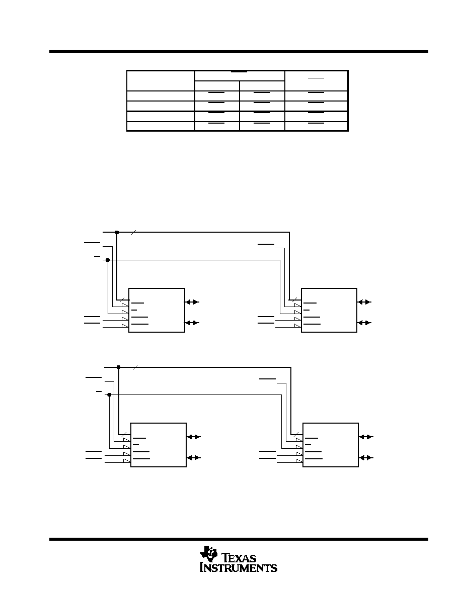
The TM124FBK32F operates as two TMS418169DZs connected as shown in the functional block diagram and
in Table 1. The TM248GBK32F operates as four TMS418169DZs connected as shown in the functional block
diagram and in Table 1. The common I / O feature dictates the use of early-write cycles to prevent contention
on D and Q.
Please be aware that an important notice concerning availability, standard warranty, and use in critical applications of
Texas Instruments semiconductor products and disclaimers thereto appears at the end of this data sheet.
Part numbers in this data sheet are for the gold-tabbed version; the information applies to both gold-tabbed and solder-tabbed versions.
PRODUCTION DATA information is current as of publication date.
Products conform to specifications per the terms of Texas Instruments
standard warranty. Production processing does not necessarily include
testing of all parameters.
Copyright
©
1996, Texas Instruments Incorporated
TM124FBK32F, TM124FBK32U 1048576 BY 32-BIT DYNAMIC RAM MODULE
TM248GBK32F, TM248GBK32U 2097152 BY 32-BIT DYNAMIC RAM MODULE
SMMS660 ≠ MARCH 1996
2
POST OFFICE BOX 1443
∑
HOUSTON, TEXAS 77251≠1443
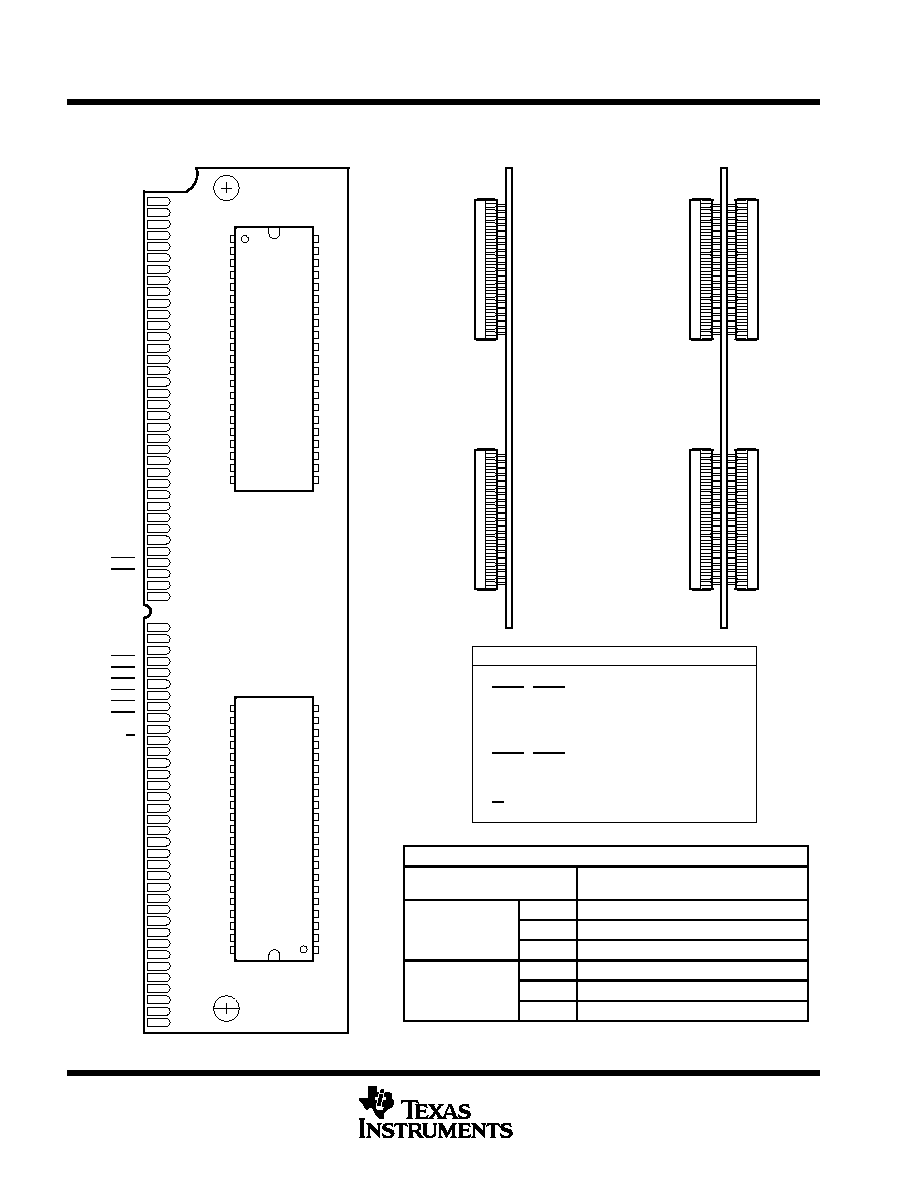
PRESENCE DETECT
SIGNAL
(PIN)
PD1
(67)
PD2
(68)
PD3
(69)
PD4
(70)
80 ns
VSS
VSS
NC
VSS
TM124FBK32F
70 ns
VSS
VSS
VSS
NC
60 ns
VSS
VSS
NC
NC
80 ns
NC
NC
NC
VSS
TM248GBK32F
70 ns
NC
NC
VSS
NC
60 ns
NC
NC
NC
NC
NC
NC
CAS0
CAS2
CAS3
CAS1
RAS0
RAS1
NC
W
NC
DQ8
DQ24
DQ9
DQ25
DQ10
DQ26
DQ11
DQ27
DQ12
DQ28
VCC
DQ29
DQ13
DQ30
DQ14
DQ31
DQ15
NC
PD1
PD2
PD3
PD4
NC
VSS
37
38
39
40
41
42
43
44
45
46
47
48
49
50
51
52
53
54
55
56
57
58
59
60
61
62
63
64
65
66
67
68
69
70
71
72
1
2
3
4
5
6
7
8
9
10
11
12
13
14
15
16
17
18
19
20
21
22
23
24
25
26
27
28
29
30
31
32
33
34
35
36
BK SINGLE IN-LINE MEMORY MODULE
( TOP VIEW )
TM124FBK32F
( SIDE VIEW )
PIN NOMENCLATURE
A0 ≠ A9
Address Inputs
CAS0 ≠ CAS3
Column-Address Strobe
DQ0 ≠ DQ31
Data In/Data Out
NC
No Connection
PD1 ≠ PD4
Presence Detects
RAS0 ≠ RAS3
Row-Address Strobe
VCC
5-V Supply
VSS
Ground
W
Write Enable
TM248GBK32F
( SIDE VIEW )
VSS
DQ0
DQ16
DQ1
DQ17
DQ2
DQ18
DQ3
DQ19
VCC
NC
A0
A1
A2
A3
A4
A5
A6
NC
DQ4
DQ20
DQ5
DQ21
DQ6
DQ22
DQ7
DQ23
A7
NC
VCC
A8
A9
RAS3
RAS2
NC
NC
VSS
TM124FBK32F, TM124FBK32U 1048576 BY 32-BIT DYNAMIC RAM MODULE
TM248GBK32F, TM248GBK32U 2097152 BY 32-BIT DYNAMIC RAM MODULE
SMMS660 ≠ MARCH 1996
3
POST OFFICE BOX 1443
∑
HOUSTON, TEXAS 77251≠1443
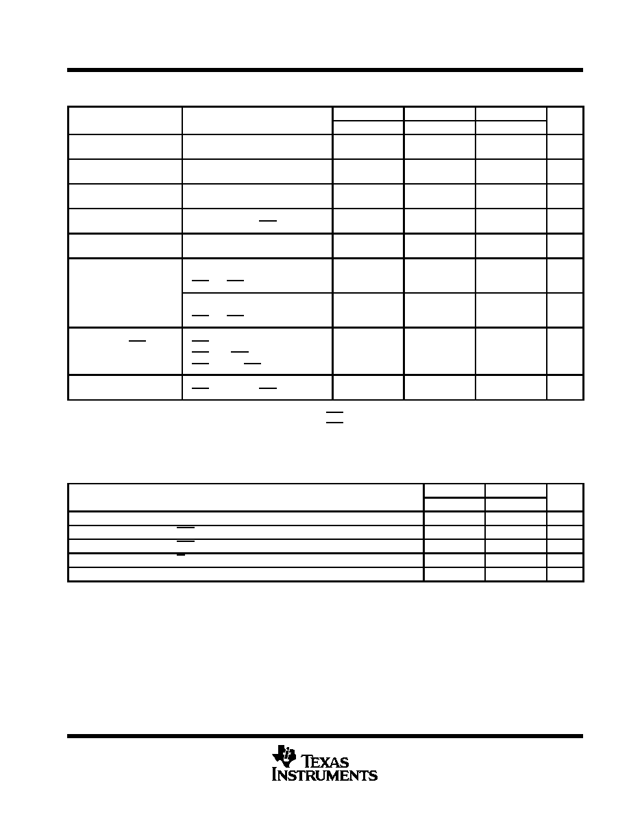
Table 1. Connection Table
DATA BLOCK
RASx
CASx
DATA BLOCK
SIDE 1
SIDE 2
CASx
DQ0 ≠ DQ7
RAS0
RAS1
CAS0
DQ8 ≠ DQ15
RAS0
RAS1
CAS1
DQ16 ≠ DQ23
RAS2
RAS3
CAS2
DQ24 ≠ DQ31
RAS2
RAS3
CAS3
Side 2 applies to the TM248GBK32F and the TM248GBK32U.
single in-line memory module and components
PC substrate: 1,27
±
0,1 mm (0.05 inch) nominal thickness; 0.005 inch / inch maximum warpage
Bypass capacitors: Multilayer ceramic
Contact area for TM124FBK32F and TM248GBK32F: Nickel plate and gold plate over copper
Contact area for TM124FBK32U and TM248GBK32U: Nickel plate and tin/lead over copper
functional block diagram ( TM124FBK32F and TM248GBK32F, side 1)
1M
◊
16
A0 ≠A9
DQ0 ≠
RAS
DQ7
W
LCAS
DQ8 ≠
UCAS
DQ15
A0 ≠ A9
DQ8 ≠ DQ15
DQ24 ≠ DQ31
W
RAS0
CAS0
CAS1
RAS2
10
10
10
DQ0 ≠ DQ7
DQ16 ≠ DQ23
1M
◊
16
A0 ≠A9
DQ0 ≠
RAS
DQ7
W
LCAS
DQ8 ≠
UCAS
DQ15
CAS2
CAS3
functional block diagram ( TM248GBK32F, side 2 )
1M
◊
16
A0 ≠A9
DQ0 ≠
RAS
DQ7
W
LCAS
DQ8 ≠
UCAS
DQ15
A0 ≠ A9
DQ0 ≠ DQ7
DQ16 ≠ DQ23
W
RAS1
CAS1
CAS0
RAS3
10
10
10
DQ8 ≠ DQ15
DQ24 ≠ DQ31
1M
◊
16
A0 ≠A9
DQ0 ≠
RAS
DQ7
W
LCAS
DQ8 ≠
UCAS
DQ15
CAS3
CAS2
TM124FBK32F, TM124FBK32U 1048576 BY 32-BIT DYNAMIC RAM MODULE
TM248GBK32F, TM248GBK32U 2097152 BY 32-BIT DYNAMIC RAM MODULE
SMMS660 ≠ MARCH 1996
4
POST OFFICE BOX 1443
∑
HOUSTON, TEXAS 77251≠1443
absolute maximum ratings over operating free-air temperature range (unless otherwise noted)
Supply voltage range, V
CC
(see Note 1)
≠ 1 V to 7 V
. . . . . . . . . . . . . . . . . . . . . . . . . . . . . . . . . . . . . . . . . . . . . .
Voltage range on any pin (see Note 1)
≠ 1 V to 7 V
. . . . . . . . . . . . . . . . . . . . . . . . . . . . . . . . . . . . . . . . . . . . . . . . .
Short-circuit output current
50 mA
. . . . . . . . . . . . . . . . . . . . . . . . . . . . . . . . . . . . . . . . . . . . . . . . . . . . . . . . . . . . . . . .
Power dissipation:
TM124FBK32F, TM124FBK32U
2 W
. . . . . . . . . . . . . . . . . . . . . . . . . . . . . . . . . . . . . . . . .
TM248GBK32F, TM248GBK32U
4 W
. . . . . . . . . . . . . . . . . . . . . . . . . . . . . . . . . . . . . . . . .
Operating free-air temperature range, T
A
0
∞
C to 70
∞
C
. . . . . . . . . . . . . . . . . . . . . . . . . . . . . . . . . . . . . . . . . . . . . .
Storage temperature range, T
stg
≠ 55
∞
C to 125
∞
C
. . . . . . . . . . . . . . . . . . . . . . . . . . . . . . . . . . . . . . . . . . . . . . . . . .
Stresses beyond those listed under "absolute maximum ratings" may cause permanent damage to the device. These are stress ratings only, and
functional operation of the device at these or any other conditions beyond those indicated under "recommended operating conditions" is not
implied. Exposure to absolute-maximum-rated conditions for extended periods may affect device reliability.
NOTE 1: All voltage values are with respect to VSS.
recommended operating conditions
MIN
NOM
MAX
UNIT
VCC
Supply voltage
4.5
5
5.5
V
VIH
High-level input voltage
2.4
6.5
V
VIL
Low-level input voltage (see Note 2)
≠ 1
0.8
V
TA
Operating free-air temperature
0
70
∞
C
NOTE 2: The algebraic convention, where the more negative (less positive) limit is designated as minimum, is used for logic-voltage levels only.
electrical characteristics over recommended ranges of supply voltage and operating free-air
temperature (unless otherwise noted)
PARAMETER
TEST CONDITIONS
'124FBK32F - 60
'124FBK32F - 70
'124FBK32F - 80
UNIT
PARAMETER
TEST CONDITIONS
MIN
MAX
MIN
MAX
MIN
MAX
UNIT
VOH High-level output voltage
IOH = ≠ 5 mA
2.4
2.4
2.4
V
VOL
Low-level output voltage
IOL = 4.2 mA
0.4
0.4
0.4
V
II
Input current (leakage)
VCC = 5.5 V, VI = 0 V to 6.5 V,
All other pins = 0 V to VCC
±
10
±
10
±
10
µ
A
IO
Output current (leakage)
VCC = 5.5 V,
VO = 0 V to VCC,
CAS high
±
10
±
10
±
10
µ
A
ICC1
Read- or write-cycle
current (see Note 3)
VCC = 5.5 V, Minimum cycle
380
360
340
mA
ICC2 Standby current
VIH = 2.4 V (TTL),
After one memory cycle,
RAS and CAS high
4
4
4
mA
ICC2 Standby current
VIH = VCC ≠ 0.2 V (CMOS),
After one memory cycle,
RAS and CAS high
2
2
2
mA
ICC3
Average refresh current
(RAS only or CBR)
(see Note 3)
VCC = 5.5 V, Minimum cycle,
RAS cycling,
CAS high (RAS only);
RAS low after CAS low (CBR)
380
360
340
mA
ICC4
Average EDO current
(see Note 4)
VCC = 5.5 V, tHPC = MIN,
RAS low,
CAS cycling
200
180
160
mA
For test conditions shown as MIN / MAX, use the appropriate value specified under recommended operating conditions.
NOTES:
3. Measured with a maximum of one address change while RAS = VIL
4. Measured with a maximum of one address change while CAS = VIH
TM124FBK32F, TM124FBK32U 1048576 BY 32-BIT DYNAMIC RAM MODULE
TM248GBK32F, TM248GBK32U 2097152 BY 32-BIT DYNAMIC RAM MODULE
SMMS660 ≠ MARCH 1996
5
POST OFFICE BOX 1443
∑
HOUSTON, TEXAS 77251≠1443
electrical characteristics over recommended ranges of supply voltage and operating free-air
temperature (unless otherwise noted) (continued)
PARAMETER
TEST CONDITIONS
'248GBK32F - 60
'248GBK32F - 70
'248GBK32F - 80
UNIT
PARAMETER
TEST CONDITIONS
MIN
MAX
MIN
MAX
MIN
MAX
UNIT
VOH
High-level output
voltage
IOH = ≠ 5 mA
2.4
2.4
2.4
V
VOL
Low-level output
voltage
IOL = 4.2 mA
0.4
0.4
0.4
V
II
Input current
(leakage)
VCC = 5.5 V,
VI = 0 V to 6.5 V,
All other pins = 0 V to VCC
±
10
±
10
±
10
µ
A
IO
Output current
(leakage)
VCC = 5.5 V,
VO = 0 V to VCC, CAS high
±
20
±
20
±
20
µ
A
ICC1
Read- or write-cycle
current (see Note 3)
VCC = 5.5 V,
Minimum cycle
384
364
344
mA
ICC2 Standby current
VIH = 2.4 V (TTL),
After one memory cycle,
RAS and CAS high
8
8
8
mA
ICC2 Standby current
VIH = VCC ≠ 0.2 V (CMOS),
After one memory cycle,
RAS and CAS high
4
4
4
mA
ICC3
Average refresh
current (RAS only or
CBR)
(see Notes 3 and 5)
VCC = 5.5 V,
Minimum cycle,
RAS cycling,
CAS high (RAS only);
RAS low after CAS low (CBR)
760
720
680
mA
ICC4
Average EDO current
(see Note 4)
VCC = 5.5 V,
tPC = MIN,
RAS low,
CAS cycling
204
184
164
mA
For test conditions shown as MIN / MAX, use the appropriate value specified under recommended operating conditions.
NOTES:
3. Measured with a maximum of one address change while RAS = VIL
4. Measured with a maximum of one address change while CAS = VIH
5. Measured with both sides in CBR cycle
capacitance over recommended ranges of supply voltage and operating free-air temperature,
f = 1 MHz (see Note 6)
PARAMETER
'124FBK32F
'248GBK32F
UNIT
PARAMETER
MIN
MAX
MIN
MAX
UNIT
Ci(A)
Input capacitance, A0 ≠ A9
12
22
pF
Ci(R)
Input capacitance, RAS inputs
8
8
pF
Ci(C)
Input capacitance, CAS inputs
8
15
pF
Ci(W)
Input capacitance, W
16
30
pF
Co(DQ) Output capacitance on DQ0 ≠ DQ31
8
15
pF
NOTE 6: VCC = 5 V
±
0.5 V, and the bias on pins under test is 0 V.