TMS370Cx5x
8-BIT MICROCONTROLLER
SPNS010F ≠ DECEMBER 1986 ≠ REVISED FEBRUARY 1997
1
POST OFFICE BOX 1443
∑
HOUSTON, TEXAS 77251≠1443
D
CMOS/EEPROM/EPROM Technologies on a
Single Device
≠ Mask-ROM Devices for High-Volume
Production
≠ One-Time-Programmable (OTP) EPROM
Devices for Low-Volume Production
≠ Reprogrammable EPROM Devices for
Prototyping Purposes
D
Internal System Memory Configurations
≠ On-Chip Program Memory Versions
≠ ROM: 4K to 48K Bytes
≠ EPROM: 16K to 48K Bytes
≠ ROM-less
≠ Data EEPROM: 256 or 512 Bytes
≠ Static RAM: 256 to 3.5K Bytes
≠ External Memory / Peripheral Wait States
≠ Precoded External Chip-Select Outputs
in Microcomputer Mode
D
Flexible Operating Features
≠ Low-Power Modes: STANDBY and HALT
≠ Commercial, Industrial, and Automotive
Temperature Ranges
≠ Clock Options
≠ Divide-by-4 (0.5 MHz ≠ 5 MHz SYSCLK)
≠ Divide-by-1 (2 MHz ≠ 5 MHz SYSCLK)
Phase-Locked Loop (PLL)
≠ Supply Voltage (V
CC
): 5 V
±
10%
D
Eight-Channel 8-Bit Analog-to-Digital
Converter 1 (ADC1)
D
Two 16-Bit General-Purpose Timers
D
On-Chip 24-Bit Watchdog Timer
D
Two Communication Modules
≠ Serial Communications Interface 1 (SCI1)
≠ Serial Peripheral Interface (SPI)
D
Flexible Interrupt Handling
D
TMS370 Series Compatibility
D
CMOS/Package /TTL-Compatible I / O Pins
≠ 64-Pin Plastic and Ceramic Shrink
Dual-In-Line Packages / 44 Bidirectional,
9 Input Pins
≠ 68-Pin Plastic and Ceramic Leaded Chip
Carrier Packages / 46 Bidirectional,
9 Input Pins
≠ All Peripheral Function Pins Are
Software Configurable for Digital I / O
D
Workstation/PC-Based Development
System
≠ C Compiler and C Source Debugger
≠ Real-Time In-Circuit Emulation
≠ Extensive Breakpoint / Trace Capability
≠ Software Performance Analysis
≠ Multi-Window User Interface
≠ Microcontroller Programmer
PRODUCTION DATA information is current as of publication date.
Products conform to specifications per the terms of Texas Instruments
standard warranty. Production processing does not necessarily include
testing of all parameters.
Copyright
©
1997, Texas Instruments Incorporated
Please be aware that an important notice concerning availability, standard warranty, and use in critical applications of
Texas Instruments semiconductor products and disclaimers thereto appears at the end of this data sheet.
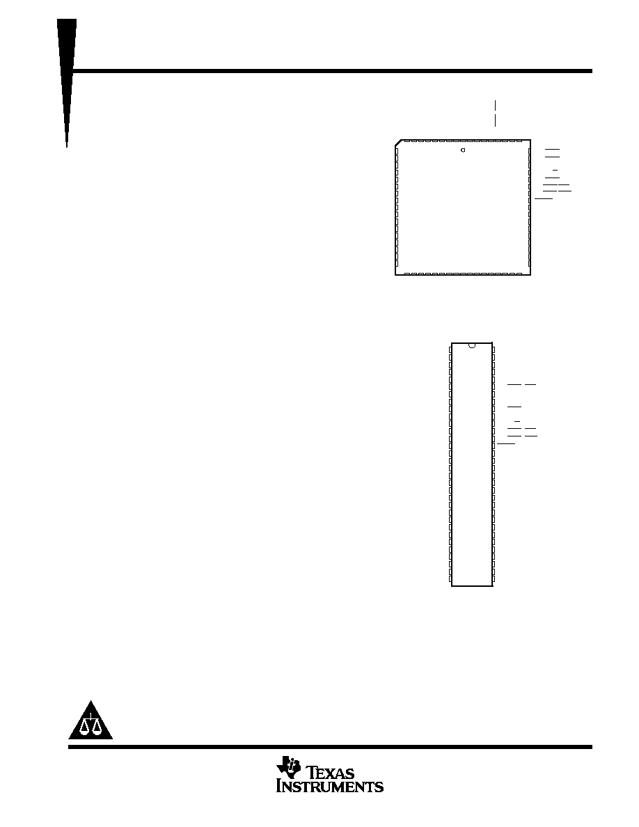
FN / FZ PACKAGE
( TOP VIEW )
V
SS1
B7
C2
C1
MC
C0
B6
T2AIC1/CR
SCICLK
SCIRXD
SCITXD
XT
AL2/CLKIN
XT
AL1
C3
C4
C5
C6
C7
SPISOMI
SPICLK
SPISIMO
T1IC/CR
T1PWM
T1EVT
9 8 7 6 5 4 3
10
11
12
13
14
15
16
B5
B0
B4
B3
B2
B1
D0
/
CSE2
/
OCF
V
CC2
V
SS2
V
CC1
2 1 68 67 66 65 64 63 62 61
27 28 29 30 31 32 33 34 35 36 37 38 39 40 41 42 43
V
CC3
V
SS3
V
CC1
17
18
19
20
21
22
23
24
25
26
60
59
58
57
56
55
54
53
52
51
50
49
48
47
46
45
44
V
CC2
V
SS2
A0
A1
A2
A3
A4
A5
A6
A7
T2AEVT
T2AIC2/PWM
INT1
INT2
INT3
D1 / CSH3
D2 / CSH2
D3 / SYSCLK
D4 / R / W
D5 / CSPF
D6/CSH1/EDS
D7/CSE1/WAIT
RESET
AN0
AN1
AN2
AN3
AN4
AN5
AN6
AN7
JN / NM PACKAGE
( TOP VIEW )
1
2
3
4
5
6
7
8
9
10
11
12
13
14
15
16
17
18
19
20
21
22
23
24
25
26
27
28
29
30
31
32
33
34
35
36
37
38
39
40
41
42
43
44
45
46
47
48
49
50
51
52
53
54
55
56
57
58
59
60
61
62
63
64
B5
B6
B7
C0
MC
C1
C2
V
SS1
C3
C4
C5
C6
C7
AN0
A0
A1
A2
A3
A4
A5
A6
A7
T2AEVT
T2AIC2 / PWM
T2AIC1 / CR
SCICLK
SCIRXD
SCITXD
XTAL2 / CLKIN
XTAL1
V
CC1
V
CC3
B4
B3
B2
B1
B0
D0 / CSE2 / OCF
V
SS1
V
CC1
D1 / CSH3
D3 / SYSCLK
D4 / R / W
D6 / CSH1 / EDS
D7 / CSE1 / WAIT
RESET
INT1
INT2
INT3
SPISOMI
SPISIMO
SPICLK
T1IC / CR
T1PWM
AN7
T1EVT
V
SS1
AN6
AN5
AN4
AN3
AN1
AN2
V
SS3
TMS370Cx5x
8-BIT MICROCONTROLLER
SPNS010F ≠ DECEMBER 1986 ≠ REVISED FEBRUARY 1997
2
POST OFFICE BOX 1443
∑
HOUSTON, TEXAS 77251≠1443
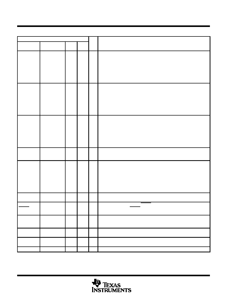
Pin Descriptions
¡¡¡¡¡¡¡¡¡¡¡¡¡¡
¡¡¡¡¡¡¡¡¡¡¡¡¡¡
PIN
¡¡
¡¡
¡¡¡¡¡¡¡¡¡¡¡¡¡¡¡¡¡¡¡¡
¡¡¡¡¡¡¡¡¡¡¡¡¡¡¡¡¡¡¡¡
¡¡¡¡¡
¡¡¡¡¡
NAME
¡¡¡¡¡¡
¡¡¡¡¡¡
ALTERNATE
FUNCTION
¡¡¡
¡¡¡
SDIP
(64)
¡¡¡
¡¡¡
LCC
(68)
¡¡
¡¡
I/O
¡¡¡¡¡¡¡¡¡¡¡¡¡¡¡¡¡¡¡¡
¡¡¡¡¡¡¡¡¡¡¡¡¡¡¡¡¡¡¡¡
DESCRIPTION
¡¡¡¡¡
¡
¡¡¡
¡
¡
¡¡¡
¡
¡
¡¡¡
¡
¡
¡¡¡
¡
¡
¡¡¡
¡
¡¡¡¡¡
A0
A1
A2
A3
A4
A5
A6
A7
¡¡¡¡¡¡
¡
¡¡¡¡
¡
¡
¡¡¡¡
¡
¡
¡¡¡¡
¡
¡
¡¡¡¡
¡
¡
¡¡¡¡
¡
¡¡¡¡¡¡
DATA0
DATA1
DATA2
DATA3
DATA4
DATA5
DATA6
DATA7
¡¡¡
¡
¡
¡
¡
¡
¡
¡
¡
¡
¡
¡
¡
¡
¡
¡
¡¡¡
15
16
17
18
19
20
21
22
¡¡¡
¡
¡
¡
¡
¡
¡
¡
¡
¡
¡
¡
¡
¡
¡
¡
¡¡¡
17
18
19
20
21
22
23
24
¡¡
¡
¡
¡
¡
¡
¡
¡
¡
¡
¡
¡¡
I / O
¡¡¡¡¡¡¡¡¡¡¡¡¡¡¡¡¡¡¡¡
¡
¡¡¡¡¡¡¡¡¡¡¡¡¡¡¡¡¡¡
¡
¡
¡¡¡¡¡¡¡¡¡¡¡¡¡¡¡¡¡¡
¡
¡
¡¡¡¡¡¡¡¡¡¡¡¡¡¡¡¡¡¡
¡
¡
¡¡¡¡¡¡¡¡¡¡¡¡¡¡¡¡¡¡
¡
¡
¡¡¡¡¡¡¡¡¡¡¡¡¡¡¡¡¡¡
¡
¡¡¡¡¡¡¡¡¡¡¡¡¡¡¡¡¡¡¡¡
Single-chip mode: Port A is a general-purpose bidirectional I/O port.
Expansion mode: Port A can be individually programmed as the external
bidirectional data bus (DATA0 ≠ DATA7).
¡¡¡¡¡
¡
¡¡¡
¡
¡
¡¡¡
¡
¡
¡¡¡
¡
¡
¡¡¡
¡
¡¡¡¡¡
B0
B1
B2
B3
B4
B5
B6
B7
¡¡¡¡¡¡
¡
¡¡¡¡
¡
¡
¡¡¡¡
¡
¡
¡¡¡¡
¡
¡
¡¡¡¡
¡
¡¡¡¡¡¡
ADDR0
ADDR1
ADDR2
ADDR3
ADDR4
ADDR5
ADDR6
ADDR7
¡¡¡
¡
¡
¡
¡
¡
¡
¡
¡
¡
¡
¡
¡
¡¡¡
60
61
62
63
64
1
2
3
¡¡¡
¡
¡
¡
¡
¡
¡
¡
¡
¡
¡
¡
¡
¡¡¡
65
66
67
68
1
2
3
4
¡¡
¡
¡
¡
¡
¡
¡
¡
¡
¡¡
I / O
¡¡¡¡¡¡¡¡¡¡¡¡¡¡¡¡¡¡¡¡
¡
¡¡¡¡¡¡¡¡¡¡¡¡¡¡¡¡¡¡
¡
¡
¡¡¡¡¡¡¡¡¡¡¡¡¡¡¡¡¡¡
¡
¡
¡¡¡¡¡¡¡¡¡¡¡¡¡¡¡¡¡¡
¡
¡
¡¡¡¡¡¡¡¡¡¡¡¡¡¡¡¡¡¡
¡
¡¡¡¡¡¡¡¡¡¡¡¡¡¡¡¡¡¡¡¡
Single-chip mode: Port B is a general-purpose bidirectional I/O port.
Expansion mode: Port B can be individually programmed as the low-order address
output bus (ADDR0 ≠ ADDR7).
¡¡¡¡¡
¡
¡¡¡
¡
¡
¡¡¡
¡
¡
¡¡¡
¡
¡
¡¡¡
¡
¡¡¡¡¡
C0
C1
C2
C3
C4
C5
C6
C7
¡¡¡¡¡¡
¡
¡¡¡¡
¡
¡
¡¡¡¡
¡
¡
¡¡¡¡
¡
¡
¡¡¡¡
¡
¡¡¡¡¡¡
ADDR8
ADDR9
ADDR10
ADDR11
ADDR12
ADDR13
ADDR14
ADDR15
¡¡¡
¡
¡
¡
¡
¡
¡
¡
¡
¡
¡
¡
¡
¡¡¡
4
6
7
9
10
11
12
13
¡¡¡
¡
¡
¡
¡
¡
¡
¡
¡
¡
¡
¡
¡
¡¡¡
5
7
8
10
11
12
13
14
¡¡
¡
¡
¡
¡
¡
¡
¡
¡
¡¡
I / O
¡¡¡¡¡¡¡¡¡¡¡¡¡¡¡¡¡¡¡¡
¡
¡¡¡¡¡¡¡¡¡¡¡¡¡¡¡¡¡¡
¡
¡
¡¡¡¡¡¡¡¡¡¡¡¡¡¡¡¡¡¡
¡
¡
¡¡¡¡¡¡¡¡¡¡¡¡¡¡¡¡¡¡
¡
¡
¡¡¡¡¡¡¡¡¡¡¡¡¡¡¡¡¡¡
¡
¡¡¡¡¡¡¡¡¡¡¡¡¡¡¡¡¡¡¡¡
Single-chip mode: Port C is a general-purpose bidirectional I/O port.
Expansion mode: Port C can be individually programmed as the high-order address
output bus (ADDR8 ≠ ADDR15).
¡¡¡¡¡
¡
¡¡¡
¡
¡
¡¡¡
¡
¡¡¡¡¡
INT1
INT2
INT3
¡¡¡¡¡¡
¡
¡¡¡¡
¡
¡
¡¡¡¡
¡
¡¡¡¡¡¡
NMI
--
--
¡¡¡
¡
¡
¡
¡
¡
¡
¡¡¡
50
49
48
¡¡¡
¡
¡
¡
¡
¡
¡
¡¡¡
52
51
50
¡¡
¡
¡
¡
¡
¡¡
I
I / O
I / O
¡¡¡¡¡¡¡¡¡¡¡¡¡¡¡¡¡¡¡¡
¡
¡¡¡¡¡¡¡¡¡¡¡¡¡¡¡¡¡¡
¡
¡
¡¡¡¡¡¡¡¡¡¡¡¡¡¡¡¡¡¡
¡
¡¡¡¡¡¡¡¡¡¡¡¡¡¡¡¡¡¡¡¡
External (nonmaskable or maskable) interrupt/general-purpose input pin
External maskable interrupt input/general-purpose bidirectional pin
External maskable interrupt input/general-purpose bidirectional pin
¡¡¡¡¡
¡
¡¡¡
¡
¡
¡¡¡
¡
¡
¡¡¡
¡
¡
¡¡¡
¡
¡¡¡¡¡
AN0
AN1
AN2
AN3
AN4
AN5
AN6
AN7
¡¡¡¡¡¡
¡
¡¡¡¡
¡
¡
¡¡¡¡
¡
¡
¡¡¡¡
¡
¡
¡¡¡¡
¡
¡¡¡¡¡¡
E0
E1
E2
E3
E4
E5
E6
E7
¡¡¡
¡
¡
¡
¡
¡
¡
¡
¡
¡
¡
¡
¡
¡¡¡
14
34
35
36
37
38
39
42
¡¡¡
¡
¡
¡
¡
¡
¡
¡
¡
¡
¡
¡
¡
¡¡¡
36
37
38
39
40
41
42
43
¡¡
¡
¡
¡
¡
¡
¡
¡
¡
¡¡
I
¡¡¡¡¡¡¡¡¡¡¡¡¡¡¡¡¡¡¡¡
¡
¡¡¡¡¡¡¡¡¡¡¡¡¡¡¡¡¡¡
¡
¡
¡¡¡¡¡¡¡¡¡¡¡¡¡¡¡¡¡¡
¡
¡
¡¡¡¡¡¡¡¡¡¡¡¡¡¡¡¡¡¡
¡
¡
¡¡¡¡¡¡¡¡¡¡¡¡¡¡¡¡¡¡
¡
¡¡¡¡¡¡¡¡¡¡¡¡¡¡¡¡¡¡¡¡
ADC1 analog input (AN0 ≠ AN7) or positive reference pins (AN1 ≠ AN7)
Port E can be individually programmed as general-purpose input pins if not used
as ADC1 analog input or positive reference input.
¡¡¡¡¡
¡
¡¡¡
¡
¡¡¡¡¡
VCC3
VSS3
¡¡¡¡¡¡
¡
¡¡¡¡
¡
¡¡¡¡¡¡
¡¡¡
¡
¡
¡
¡¡¡
32
33
¡¡¡
¡
¡
¡
¡¡¡
34
35
¡¡
¡
¡
¡¡
¡¡¡¡¡¡¡¡¡¡¡¡¡¡¡¡¡¡¡¡
¡
¡¡¡¡¡¡¡¡¡¡¡¡¡¡¡¡¡¡
¡
¡¡¡¡¡¡¡¡¡¡¡¡¡¡¡¡¡¡¡¡
ADC1 positive-supply voltage and optional positive-reference input pin
ADC1 ground reference pin
¡¡¡¡¡
¡
¡¡¡
¡
¡¡¡¡¡
RESET
¡¡¡¡¡¡
¡
¡¡¡¡
¡
¡¡¡¡¡¡
¡¡¡
¡
¡
¡
¡¡¡
51
¡¡¡
¡
¡
¡
¡¡¡
53
¡¡
¡
¡
¡¡
I / O
¡¡¡¡¡¡¡¡¡¡¡¡¡¡¡¡¡¡¡¡
¡
¡¡¡¡¡¡¡¡¡¡¡¡¡¡¡¡¡¡
¡
¡¡¡¡¡¡¡¡¡¡¡¡¡¡¡¡¡¡¡¡
System reset bidirectional pin. RESET, as an input, initializes the microcontroller;
as open-drain output, RESET indicates an internal failure was detected by the
watchdog or oscillator fault circuit.
¡¡¡¡¡
¡
¡¡¡
¡
¡¡¡¡¡
MC
¡¡¡¡¡¡
¡
¡¡¡¡
¡
¡¡¡¡¡¡
¡¡¡
¡
¡
¡
¡¡¡
5
¡¡¡
¡
¡
¡
¡¡¡
6
¡¡
¡
¡
¡¡
I
¡¡¡¡¡¡¡¡¡¡¡¡¡¡¡¡¡¡¡¡
¡
¡¡¡¡¡¡¡¡¡¡¡¡¡¡¡¡¡¡
¡
¡¡¡¡¡¡¡¡¡¡¡¡¡¡¡¡¡¡¡¡
Mode control (MC) pin. MC enables EEPROM write-protection override (WPO)
mode, also EPROM VPP.
¡¡¡¡¡
¡
¡¡¡
¡
¡¡¡¡¡
XTAL2/CLKIN
XTAL1
¡¡¡¡¡¡
¡
¡¡¡¡
¡
¡¡¡¡¡¡
¡¡¡
¡
¡
¡
¡¡¡
29
30
¡¡¡
¡
¡
¡
¡¡¡
31
32
¡¡
¡
¡
¡¡
I
O
¡¡¡¡¡¡¡¡¡¡¡¡¡¡¡¡¡¡¡¡
¡
¡¡¡¡¡¡¡¡¡¡¡¡¡¡¡¡¡¡
¡
¡¡¡¡¡¡¡¡¡¡¡¡¡¡¡¡¡¡¡¡
Internal oscillator crystal input / external clock source input
Internal oscillator output for crystal
¡¡¡¡¡
¡¡¡¡¡
VCC1
¡¡¡¡¡¡
¡¡¡¡¡¡
¡¡¡
¡¡¡
31, 57
¡¡¡
¡¡¡
33,
61
¡¡
¡¡
¡¡¡¡¡¡¡¡¡¡¡¡¡¡¡¡¡¡¡¡
¡¡¡¡¡¡¡¡¡¡¡¡¡¡¡¡¡¡¡¡
Positive supply voltage
¡¡¡¡¡
¡¡¡¡¡
VCC2
¡¡¡¡¡¡
¡¡¡¡¡¡
¡¡¡
¡¡¡
--
¡¡¡
¡¡¡
15,63
¡¡
¡¡
¡¡¡¡¡¡¡¡¡¡¡¡¡¡¡¡¡¡¡¡
¡¡¡¡¡¡¡¡¡¡¡¡¡¡¡¡¡¡¡¡
Positive supply voltage
I = input, O = output
Ports A, B, C, and D can be configured only as general-purpose I/O pins. Also, port D3 can be configured as SYSCLK.
TMS370Cx5x
8-BIT MICROCONTROLLER
SPNS010F ≠ DECEMBER 1986 ≠ REVISED FEBRUARY 1997
3
POST OFFICE BOX 1443
∑
HOUSTON, TEXAS 77251≠1443
Pin Descriptions (Continued)
¡¡¡¡¡¡¡¡¡¡¡¡¡¡
¡¡¡¡¡¡¡¡¡¡¡¡¡¡
PIN
¡¡
¡¡
¡¡¡¡¡¡¡¡¡¡¡¡¡¡¡¡¡¡¡
¡¡¡¡¡¡¡¡¡¡¡¡¡¡¡¡¡¡¡
¡¡¡¡¡
¡
¡¡¡
¡
¡¡¡¡¡
NAME
¡¡¡¡¡¡
¡
¡¡¡¡
¡
¡¡¡¡¡¡
ALTERNATE
FUNCTION
¡¡¡
¡
¡
¡
¡¡¡
SDIP
(64)
¡¡¡
¡
¡
¡
¡¡¡
LCC
(68)
¡¡
¡¡
¡¡
I/O
¡¡¡¡¡¡¡¡¡¡¡¡¡¡¡¡¡¡¡
¡
¡¡¡¡¡¡¡¡¡¡¡¡¡¡¡¡¡
¡
¡¡¡¡¡¡¡¡¡¡¡¡¡¡¡¡¡¡¡
DESCRIPTION
¡¡¡¡¡
¡¡¡¡¡
VSS1
¡¡¡
¡¡¡
¡¡¡¡
¡¡¡¡
¡¡¡
¡¡¡
8,
58,40
¡¡¡
¡¡¡
9
¡¡
¡¡
¡¡¡¡¡¡¡¡¡¡¡¡¡¡¡¡¡¡¡
¡¡¡¡¡¡¡¡¡¡¡¡¡¡¡¡¡¡¡
Ground reference for digital logic
¡¡¡¡¡
¡¡¡¡¡
VSS2
¡¡¡
¡¡¡
¡¡¡¡
¡¡¡¡
¡¡¡
¡¡¡
--
¡¡¡
¡¡¡
16,62
¡¡
¡¡
¡¡¡¡¡¡¡¡¡¡¡¡¡¡¡¡¡¡¡
¡¡¡¡¡¡¡¡¡¡¡¡¡¡¡¡¡¡¡
Ground reference for digital I / O logic
¡¡¡¡¡
¡
¡¡¡
¡
¡¡¡¡¡
¡¡¡¡¡¡
¡
¡¡¡¡
¡
¡¡¡¡¡¡
FUNCTION
¡¡¡
¡
¡
¡
¡¡¡
¡¡¡
¡
¡
¡
¡¡¡
¡¡
¡¡
¡¡
¡¡¡¡¡¡¡¡¡¡¡¡¡¡¡¡¡¡¡
¡
¡¡¡¡¡¡¡¡¡¡¡¡¡¡¡¡¡
¡
¡¡¡¡¡¡¡¡¡¡¡¡¡¡¡¡¡¡¡
Single-chip mode: Port D is a general-purpose bidirectional I / O port. Each of
the port D pins can be individually configured as a general-purpose I / O pin,
primary memory control signal (function A) or secondary memory control
¡¡¡¡¡
¡
¡¡¡
¡
¡¡¡¡¡
¡¡¡
¡
¡
¡
¡¡¡
A
¡¡¡¡
¡
¡¡
¡
¡¡¡¡
B
¡¡¡
¡
¡
¡
¡¡¡
¡¡¡
¡
¡
¡
¡¡¡
¡¡
¡¡
¡¡
¡¡¡¡¡¡¡¡¡¡¡¡¡¡¡¡¡¡¡
¡
¡¡¡¡¡¡¡¡¡¡¡¡¡¡¡¡¡
¡
¡¡¡¡¡¡¡¡¡¡¡¡¡¡¡¡¡¡¡
primary memory control signal (function A), or secondary memory control
signal (function B). All chip selects are independent and can be used for
memory bank switching. Refer to Table 1 for function A memory accesses.
¡¡¡¡¡
¡¡¡¡¡
D0
¡¡¡
¡¡¡
CSE2
¡¡¡¡
¡¡¡¡
OCF
¡¡¡
¡¡¡
59
¡¡¡
¡¡¡
64
¡¡
¡¡
¡¡¡¡¡¡¡¡¡¡¡¡¡¡¡¡¡¡¡
¡¡¡¡¡¡¡¡¡¡¡¡¡¡¡¡¡¡¡
I / O pin A: Chip select eighth output 2 goes low during memory accesses
I / O pin B: Opcode fetch goes low during the opcode fetch memory cycle.
¡¡¡¡¡
¡
¡¡¡
¡
¡¡¡¡¡
D1
¡¡¡
¡
¡
¡
¡¡¡
CSH3
¡¡¡¡
¡
¡¡
¡
¡¡¡¡
--
¡¡¡
¡
¡
¡
¡¡¡
56
¡¡¡
¡
¡
¡
¡¡¡
60
¡¡
¡¡
¡¡
¡¡¡¡¡¡¡¡¡¡¡¡¡¡¡¡¡¡¡
¡
¡¡¡¡¡¡¡¡¡¡¡¡¡¡¡¡¡
¡
¡¡¡¡¡¡¡¡¡¡¡¡¡¡¡¡¡¡¡
I / O pin A: Chip select half output 3 goes low during memory accesses.
I / O pin B: Reserved
¡¡¡¡¡
¡
¡¡¡
¡
¡¡¡¡¡
D2
¡¡¡
¡
¡
¡
¡¡¡
CSH2
¡¡¡¡
¡
¡¡
¡
¡¡¡¡
--
¡¡¡
¡
¡
¡
¡¡¡
--
¡¡¡
¡
¡
¡
¡¡¡
59
¡¡
¡¡
¡¡
¡¡¡¡¡¡¡¡¡¡¡¡¡¡¡¡¡¡¡
¡
¡¡¡¡¡¡¡¡¡¡¡¡¡¡¡¡¡
¡
¡¡¡¡¡¡¡¡¡¡¡¡¡¡¡¡¡¡¡
I / O pin A: Chip select half output 2 goes low during memory accesses.
I / O pin B: Reserved
¡¡¡¡¡
D3
¡¡¡
SYSCLK
¡¡¡¡
SYSCLK
¡¡¡
55
¡¡¡
58
¡¡
¡¡¡¡¡¡¡¡¡¡¡¡¡¡¡¡¡¡¡
I / O pin A, B: Internal clock signal is 1 / 1 (PLL) or 1 / 4 XTAL2 / CLKIN frequency.
¡¡¡¡¡
¡¡¡¡¡
D4
¡¡¡
¡¡¡
R / W
¡¡¡¡
¡¡¡¡
R / W
¡¡¡
¡¡¡
54
¡¡¡
¡¡¡
57
¡¡
¡¡
I / O
¡¡¡¡¡¡¡¡¡¡¡¡¡¡¡¡¡¡¡
¡¡¡¡¡¡¡¡¡¡¡¡¡¡¡¡¡¡¡
I / O pin A, B: Read / write output pin
¡¡¡¡¡
¡
¡¡¡
¡
¡¡¡¡¡
D5
¡¡¡
¡
¡
¡
¡¡¡
CSPF
¡¡¡¡
¡
¡¡
¡
¡¡¡¡
--
¡¡¡
¡
¡
¡
¡¡¡
--
¡¡¡
¡
¡
¡
¡¡¡
56
¡¡
¡¡
¡¡
I / O
¡¡¡¡¡¡¡¡¡¡¡¡¡¡¡¡¡¡¡
¡
¡¡¡¡¡¡¡¡¡¡¡¡¡¡¡¡¡
¡
¡¡¡¡¡¡¡¡¡¡¡¡¡¡¡¡¡¡¡
I / O pin A: Chip select peripheral output for peripheral file goes low during
memory accesses.
I / O pin B: Reserved
¡¡¡¡¡
¡
¡¡¡
¡
¡
¡¡¡
¡
¡¡¡¡¡
D6
¡¡¡
¡
¡
¡
¡
¡
¡
¡¡¡
CSH1
¡¡¡¡
¡
¡¡
¡
¡
¡¡
¡
¡¡¡¡
EDS
¡¡¡
¡
¡
¡
¡
¡
¡
¡¡¡
53
¡¡¡
¡
¡
¡
¡
¡
¡
¡¡¡
55
¡¡
¡¡
¡¡
¡¡
¡¡¡¡¡¡¡¡¡¡¡¡¡¡¡¡¡¡¡
¡
¡¡¡¡¡¡¡¡¡¡¡¡¡¡¡¡¡
¡
¡
¡¡¡¡¡¡¡¡¡¡¡¡¡¡¡¡¡
¡
¡¡¡¡¡¡¡¡¡¡¡¡¡¡¡¡¡¡¡
I / O pin A: Chip select half output 1 goes low during memory accesses.
I / O pin B: External data strobe output goes low during memory accesses from
external memory and has the same timings as the five chip selects.
¡¡¡¡¡
¡¡¡¡¡
D7
¡¡¡
¡¡¡
CSE1
¡¡¡¡
¡¡¡¡
WAIT
¡¡¡
¡¡¡
52
¡¡¡
¡¡¡
54
¡¡
¡¡
¡¡¡¡¡¡¡¡¡¡¡¡¡¡¡¡¡¡¡
¡¡¡¡¡¡¡¡¡¡¡¡¡¡¡¡¡¡¡
I / O pin A: Chip select eighth output goes low during memory accesses.
I / O pin B: Wait input pin extends bus signals.
¡¡¡¡¡
¡
¡¡¡
¡
¡¡¡¡¡
SCITXD
SCIRXD
SCICLK
¡¡¡¡¡¡
¡
¡¡¡¡
¡
¡¡¡¡¡¡
SCIIO1
SCIIO2
SCIIO3
¡¡¡
¡
¡
¡
¡¡¡
28
27
26
¡¡¡
¡
¡
¡
¡¡¡
30
29
28
¡¡
¡¡
¡¡
I / O
¡¡¡¡¡¡¡¡¡¡¡¡¡¡¡¡¡¡¡
¡
¡¡¡¡¡¡¡¡¡¡¡¡¡¡¡¡¡
¡
¡¡¡¡¡¡¡¡¡¡¡¡¡¡¡¡¡¡¡
SCI transmit data output pin / general-purpose bidirectional pin (see Note 1)
SCI receive data input pin / general-purpose bidirectional pin
SCI bidirectional serial clock pin / general-purpose bidirectional pin
¡¡¡¡¡
¡
¡¡¡
¡
¡
¡¡¡
¡
¡
¡¡¡
¡
¡¡¡¡¡
T1IC / CR
T1PWM
T1EVT
¡¡¡¡¡¡
¡
¡¡¡¡
¡
¡
¡¡¡¡
¡
¡
¡¡¡¡
¡
¡¡¡¡¡¡
T1IO1
T1IO2
T1IO3
¡¡¡
¡
¡
¡
¡
¡
¡
¡
¡
¡
¡¡¡
44
43
41
¡¡¡
¡
¡
¡
¡
¡
¡
¡
¡
¡
¡¡¡
46
45
44
¡¡
¡¡
¡¡
¡¡
¡¡
I / O
¡¡¡¡¡¡¡¡¡¡¡¡¡¡¡¡¡¡¡
¡
¡¡¡¡¡¡¡¡¡¡¡¡¡¡¡¡¡
¡
¡
¡¡¡¡¡¡¡¡¡¡¡¡¡¡¡¡¡
¡
¡
¡¡¡¡¡¡¡¡¡¡¡¡¡¡¡¡¡
¡
¡¡¡¡¡¡¡¡¡¡¡¡¡¡¡¡¡¡¡
Timer1 input capture / counter reset input pin / general-purpose bidirectional
pin
Timer1 pulse-width-modulation (PWM) output pin / general-purpose
bidirectional pin
Timer1 external event input pin / general-purpose bidirectional pin
¡¡¡¡¡
¡
¡¡¡
¡
¡
¡¡¡
¡
¡¡¡¡¡
T2AIC1 / CR
T2AIC2 / PWM
T2AEVT
¡¡¡¡¡¡
¡
¡¡¡¡
¡
¡
¡¡¡¡
¡
¡¡¡¡¡¡
T2AIO1
T2AIO2
T2AIO3
¡¡¡
¡
¡
¡
¡
¡
¡
¡¡¡
25
24
23
¡¡¡
¡
¡
¡
¡
¡
¡
¡¡¡
27
26
25
¡¡
¡¡
¡¡
¡¡
I / O
¡¡¡¡¡¡¡¡¡¡¡¡¡¡¡¡¡¡¡
¡
¡¡¡¡¡¡¡¡¡¡¡¡¡¡¡¡¡
¡
¡
¡¡¡¡¡¡¡¡¡¡¡¡¡¡¡¡¡
¡
¡¡¡¡¡¡¡¡¡¡¡¡¡¡¡¡¡¡¡
Timer2A input capture 1 / counter reset input pin / general-purpose bidirectional
pin
Timer2A input capture 2 / PWM output pin / general-purpose bidirectional pin
Timer2A external event input pin / general-purpose bidirectional pin
¡¡¡¡¡
¡
¡¡¡
¡
¡¡¡¡¡
SPISOMI
SPISIMO
SPICLK
¡¡¡¡¡¡
¡
¡¡¡¡
¡
¡¡¡¡¡¡
SPIIO1
SPIIO2
SPIIO3
¡¡¡
¡
¡
¡
¡¡¡
47
46
45
¡¡¡
¡
¡
¡
¡¡¡
49
48
47
¡¡
¡¡
¡¡
I / O
¡¡¡¡¡¡¡¡¡¡¡¡¡¡¡¡¡¡¡
¡
¡¡¡¡¡¡¡¡¡¡¡¡¡¡¡¡¡
¡
¡¡¡¡¡¡¡¡¡¡¡¡¡¡¡¡¡¡¡
SPI slave output pin, master input pin / general-purpose bidirectional pin
SPI slave input pin, master output pin / general-purpose bidirectional pin
SPI bidirectional serial clock pin / general-purpose bidirectional pin
I = input, O = output
Ports A, B, C, and D can be configured only as general-purpose I/O pins. Port D3 also can be configured as SYSCLK.
NOTE 1: The three-pin configuration SCI is referred to as SCI1.
Table 1. Function A: Memory Accesses Locations for `x5x Devices
¡¡¡¡¡¡¡¡¡
¡¡¡¡¡¡¡¡¡
FUNCTION A
¡¡¡¡¡¡¡¡¡
¡¡¡¡¡¡¡¡¡
`X50, `X52, `X53, AND `X56
¡¡¡¡¡¡¡¡¡
¡¡¡¡¡¡¡¡¡
`X58
¡¡¡¡¡¡¡¡¡
¡¡¡¡¡¡¡¡¡
`X59
¡¡¡¡¡¡¡¡¡
¡¡¡¡¡¡¡¡¡
CSEx
¡¡¡¡¡¡¡¡¡
¡¡¡¡¡¡¡¡¡
2000h ≠ 3FFFh (8K bytes)
¡¡¡¡¡¡¡¡¡
¡¡¡¡¡¡¡¡¡
A000h ≠ BFFFh (8K bytes)
¡¡¡¡¡¡¡¡¡
¡¡¡¡¡¡¡¡¡
E000h ≠ EFFFh (4K bytes)
¡¡¡¡¡¡¡¡¡
¡¡¡¡¡¡¡¡¡
CSHx
¡¡¡¡¡¡¡¡¡
¡¡¡¡¡¡¡¡¡
8000h ≠ FFFFh (32K bytes)
¡¡¡¡¡¡¡¡¡
¡¡¡¡¡¡¡¡¡
C000h ≠ FFFFh (16K bytes)
¡¡¡¡¡¡¡¡¡
¡¡¡¡¡¡¡¡¡
F000h ≠ FFFFh (4K bytes)
¡¡¡¡¡¡¡¡¡
CSPF
¡¡¡¡¡¡¡¡¡
10C0h ≠ 10FFh (64 bytes)
¡¡¡¡¡¡¡¡¡
10C0h ≠ 10FFh (64 bytes)
¡¡¡¡¡¡¡¡¡
10C0h ≠ 10FFh (64 bytes)
TMS370Cx5x
8-BIT MICROCONTROLLER
SPNS010F ≠ DECEMBER 1986 ≠ REVISED FEBRUARY 1997
4
POST OFFICE BOX 1443
∑
HOUSTON, TEXAS 77251≠1443
functional block diagram
Program Memory
ROM: 4K, 8K, 12K, 16K,
32K, or 48K Bytes
EPROM: 16K, 32K, or
48K Bytes
VSS1
VCC1
RESET
MC
XTAL2/
CLKIN
XTAL1
INT3
INT2
INT1
E0 ≠ E7
or
AN0 ≠ AN7
VCC2
VSS2
Data EEPROM
0, 256, or 512 Bytes
RAM
256, 512, 1K, 1.5K, or
3.5K Bytes
CPU
Port D
Port C
Port B
Watchdog
Timer 1
Timer 2A
Serial
Communications
Interface 1
Serial
Peripheral
Interface
Analog-to-Digital
Converter 1
System Control
Clock Options:
Divide-by-4 or
Divide-by-1(PLL)
T1PWM
T1EVT
T1IC / CR
T2AIC2 / PWM
T2AEVT
T2AIC1 / CR
SCICLK
SCITXD
SCIRXD
SPICLK
SPISIMO
SPISOMI
VSS3
VCC3
Port A
Interrupts
8/6
8
8
8
Memory Expansion
Data
Address LSbyte
Address MSbyte
Control
For the 64-pin devices, there are only six pins for port D.
description
The TMS370Cx5x family of single-chip 8-bit microcontrollers provides cost-effective real-time system control
through integration of advanced peripheral function modules and various on-chip memory configurations. The
TMS370Cx5x family presently consists of twenty-one devices which are grouped into seven main sub-families:
the TMS370Cx50, TMS370Cx52, TMS370Cx53, TMS370Cx56, TMS370Cx58, TMS370Cx59, and
SE370C75x.
The TMS370Cx5x family of devices is implemented using high-performance silicon-gate CMOS EPROM and
EEPROM technologies. The low-operating power, wide-operating temperature range, and noise immunity of
CMOS technology, coupled with the high performance and extensive on-chip peripheral functions, make the
TMS370Cx5x devices attractive in system designs for automotive electronics, industrial motor control,
computer peripheral control, telecommunications, and consumer application. Table 2 provides a memory
configuration overview of the TMS370Cx5x devices.
TMS370Cx5x
8-BIT MICROCONTROLLER
SPNS010F ≠ DECEMBER 1986 ≠ REVISED FEBRUARY 1997
5
POST OFFICE BOX 1443
∑
HOUSTON, TEXAS 77251≠1443
description (continued)
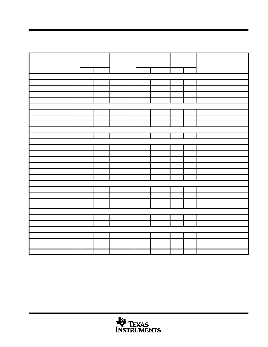
Table 2. Memory Configurations
DEVICE
PROGRAM
MEMORY
(BYTES)
OFF-CHIP
MEMORY
EXP (BYTES)
DATA MEMORY
(BYTES)
OPERATING
MODES
PACKAGES
68 PIN PLCC/CLCC, OR
64 PIN PSDIP/CSDIP
ROM
EPROM
EXP. (BYTES)
RAM
EEPROM
µ
C
µ
P
64 PIN PSDIP/CSDIP
TMS370Cx50: TMS370C050, TMS370C150, TMS370C250, AND TMS370C350
¡¡¡¡¡¡¡¡
¡¡¡¡¡¡¡¡
TMS370C050A
¡¡¡
¡¡¡
4K
¡¡¡¡
¡¡¡¡
--
¡¡¡¡¡
¡¡¡¡¡
112K
¡¡¡
¡¡¡
256
¡¡¡¡
¡¡¡¡
256
¡¡¡
¡¡¡
¡¡¡
¡¡¡
¡¡¡¡¡¡¡¡
¡¡¡¡¡¡¡¡
FN ≠ PLCC / NM ≠PSDIP
¡¡¡¡¡¡¡¡
¡¡¡¡¡¡¡¡
TMS370C150A
¡¡¡
¡¡¡
--
¡¡¡¡
¡¡¡¡
--
¡¡¡¡¡
¡¡¡¡¡
56K
¡¡¡
¡¡¡
256
¡¡¡¡
¡¡¡¡
--
¡¡¡
¡¡¡
--
¡¡¡
¡¡¡
¡¡¡¡¡¡¡¡
¡¡¡¡¡¡¡¡
FN ≠ PLCC
¡¡¡¡¡¡¡¡
¡¡¡¡¡¡¡¡
TMS370C250A
¡¡¡
¡¡¡
--
¡¡¡¡
¡¡¡¡
--
¡¡¡¡¡
¡¡¡¡¡
56K
¡¡¡
¡¡¡
256
¡¡¡¡
¡¡¡¡
256
¡¡¡
¡¡¡
--
¡¡¡
¡¡¡
¡¡¡¡¡¡¡¡
¡¡¡¡¡¡¡¡
FN ≠ PLCC
¡¡¡¡¡¡¡¡
¡¡¡¡¡¡¡¡
TMS370C350A
¡¡¡
¡¡¡
4K
¡¡¡¡
¡¡¡¡
--
¡¡¡¡¡
¡¡¡¡¡
112K
¡¡¡
¡¡¡
256
¡¡¡¡
¡¡¡¡
--
¡¡¡
¡¡¡
¡¡¡
¡¡¡
¡¡¡¡¡¡¡¡
¡¡¡¡¡¡¡¡
FN ≠ PLCC / NM ≠PSDIP
TMS370Cx52: TMS370C052, TMS370C352, AND TMS370C452
¡¡¡¡¡¡¡¡
¡¡¡¡¡¡¡¡
TMS370C052A
¡¡¡
¡¡¡
8K
¡¡¡¡
¡¡¡¡
--
¡¡¡¡¡
¡¡¡¡¡
112K
¡¡¡
¡¡¡
256
¡¡¡¡
¡¡¡¡
256
¡¡¡
¡¡¡
¡¡¡
¡¡¡
¡¡¡¡¡¡¡¡
¡¡¡¡¡¡¡¡
FN ≠ PLCC / NM ≠PSDIP
¡¡¡¡¡¡¡¡
TMS370C352A
¡¡¡
8K
¡¡¡¡
--
¡¡¡¡¡
112K
¡¡¡
256
¡¡¡¡
--
¡¡¡
¡¡¡
¡¡¡¡¡¡¡¡
FN ≠ PLCC / NM ≠PSDIP
¡¡¡¡¡¡¡¡
¡¡¡¡¡¡¡¡
TMS370C452A
¡¡¡
¡¡¡
8K
¡¡¡¡
¡¡¡¡
--
¡¡¡¡¡
¡¡¡¡¡
112K
¡¡¡
¡¡¡
256
¡¡¡¡
¡¡¡¡
256
¡¡¡
¡¡¡
¡¡¡
¡¡¡
¡¡¡¡¡¡¡¡
¡¡¡¡¡¡¡¡
FN ≠ PLCC
TMS370Cx53: TMS370C353
¡¡¡¡¡¡¡¡
¡¡¡¡¡¡¡¡
TMS370C353A
¡¡¡
¡¡¡
12K
¡¡¡¡
¡¡¡¡
--
¡¡¡¡¡
¡¡¡¡¡
112K
¡¡¡
¡¡¡
1.5K
¡¡¡¡
¡¡¡¡
--
¡¡¡
¡¡¡
¡¡¡
¡¡¡
¡¡¡¡¡¡¡¡
¡¡¡¡¡¡¡¡
FN ≠ PLCC
TMS370Cx56: TMS370C056, TMS370C156, TMS370C256, TMS370C356, TMS370C456, AND TMS370C756
¡¡¡¡¡¡¡¡
¡¡¡¡¡¡¡¡
TMS370C056A
¡¡¡
¡¡¡
16K
¡¡¡¡
¡¡¡¡
--
¡¡¡¡¡
¡¡¡¡¡
112K
¡¡¡
¡¡¡
512
¡¡¡¡
¡¡¡¡
512
¡¡¡
¡¡¡
¡¡¡
¡¡¡
¡¡¡¡¡¡¡¡
¡¡¡¡¡¡¡¡
FN ≠ PLCC / NM ≠PSDIP
¡¡¡¡¡¡¡¡
¡¡¡¡¡¡¡¡
TMS370C156A
¡¡¡
¡¡¡
--
¡¡¡¡
¡¡¡¡
--
¡¡¡¡¡
¡¡¡¡¡
56K
¡¡¡
¡¡¡
512
¡¡¡¡
¡¡¡¡
--
¡¡¡
¡¡¡
--
¡¡¡
¡¡¡
¡¡¡¡¡¡¡¡
¡¡¡¡¡¡¡¡
FN ≠ PLCC
¡¡¡¡¡¡¡¡
¡¡¡¡¡¡¡¡
TMS370C256A
¡¡¡
¡¡¡
--
¡¡¡¡
¡¡¡¡
--
¡¡¡¡¡
¡¡¡¡¡
56K
¡¡¡
¡¡¡
512
¡¡¡¡
¡¡¡¡
512
¡¡¡
¡¡¡
--
¡¡¡
¡¡¡
¡¡¡¡¡¡¡¡
¡¡¡¡¡¡¡¡
FN ≠ PLCC
¡¡¡¡¡¡¡¡
¡¡¡¡¡¡¡¡
TMS370C356A
¡¡¡
¡¡¡
16K
¡¡¡¡
¡¡¡¡
--
¡¡¡¡¡
¡¡¡¡¡
112K
¡¡¡
¡¡¡
512
¡¡¡¡
¡¡¡¡
--
¡¡¡
¡¡¡
¡¡¡
¡¡¡
¡¡¡¡¡¡¡¡
¡¡¡¡¡¡¡¡
FN ≠ PLCC / NM ≠PSDIP
¡¡¡¡¡¡¡¡
TMS370C456A
¡¡¡
16K
¡¡¡¡
--
¡¡¡¡¡
112K
¡¡¡
512
¡¡¡¡
512
¡¡¡
¡¡¡
¡¡¡¡¡¡¡¡
FN ≠ PLCC
¡¡¡¡¡¡¡¡
¡¡¡¡¡¡¡¡
TMS370C756A
¡¡¡
¡¡¡
--
¡¡¡¡
¡¡¡¡
16K
¡¡¡¡¡
¡¡¡¡¡
112K
¡¡¡
¡¡¡
512
¡¡¡¡
¡¡¡¡
512
¡¡¡
¡¡¡
¡¡¡
¡¡¡
¡¡¡¡¡¡¡¡
¡¡¡¡¡¡¡¡
FN ≠ PLCC / NM ≠PSDIP
TMS370Cx58: TMS370C058, TMS370C358, AND TMS370C758
¡¡¡¡¡¡¡¡
¡¡¡¡¡¡¡¡
TMS370C058A
¡¡¡
¡¡¡
32K
¡¡¡¡
¡¡¡¡
--
¡¡¡¡¡
¡¡¡¡¡
64K
¡¡¡
¡¡¡
1K
¡¡¡¡
¡¡¡¡
256
¡¡¡
¡¡¡
¡¡¡
¡¡¡
¡¡¡¡¡¡¡¡
¡¡¡¡¡¡¡¡
FN ≠ PLCC / NM ≠PSDIP
¡¡¡¡¡¡¡¡
¡¡¡¡¡¡¡¡
TMS370C358A
¡¡¡
¡¡¡
32K
¡¡¡¡
¡¡¡¡
--
¡¡¡¡¡
¡¡¡¡¡
64K
¡¡¡
¡¡¡
1K
¡¡¡¡
¡¡¡¡
--
¡¡¡
¡¡¡
¡¡¡
¡¡¡
¡¡¡¡¡¡¡¡
¡¡¡¡¡¡¡¡
FN ≠ PLCC / NM ≠PSDIP
¡¡¡¡¡¡¡¡
¡
¡¡¡¡¡¡
¡
¡¡¡¡¡¡¡¡
TMS370C758A,
TMS370C758B
¡¡¡
¡
¡
¡
¡¡¡
--
¡¡¡¡
¡
¡¡
¡
¡¡¡¡
32K
¡¡¡¡¡
¡
¡¡¡
¡
¡¡¡¡¡
64K
¡¡¡
¡
¡
¡
¡¡¡
1K
¡¡¡¡
¡
¡¡
¡
¡¡¡¡
256
¡¡¡
¡
¡
¡
¡¡¡
¡¡¡
¡
¡
¡
¡¡¡
¡¡¡¡¡¡¡¡
¡
¡¡¡¡¡¡
¡
¡¡¡¡¡¡¡¡
FN ≠ PLCC / NM ≠PSDIP
TMS370Cx59: TMS370C059 AND TMS370C759
¡¡¡¡¡¡¡¡
¡¡¡¡¡¡¡¡
TMS370C059Aß
¡¡¡
¡¡¡
48K
¡¡¡¡
¡¡¡¡
--
¡¡¡¡¡
¡¡¡¡¡
20K
¡¡¡
¡¡¡
3.5K
¡¡¡¡
¡¡¡¡
256
¡¡¡
¡¡¡
¡¡¡
¡¡¡
¡¡¡¡¡¡¡¡
¡¡¡¡¡¡¡¡
FN ≠ PLCC
¡¡¡¡¡¡¡¡
¡¡¡¡¡¡¡¡
TMS370C759Aß
¡¡¡
¡¡¡
--
¡¡¡¡
¡¡¡¡
48K
¡¡¡¡¡
¡¡¡¡¡
20K
¡¡¡
¡¡¡
3.5K
¡¡¡¡
¡¡¡¡
256
¡¡¡
¡¡¡
¡¡¡
¡¡¡
¡¡¡¡¡¡¡¡
¡¡¡¡¡¡¡¡
FN ≠ PLCC
EPROM DEVICE: SE370C756, SE370C758, and SE370C759
¡¡¡¡¡¡¡¡
¡¡¡¡¡¡¡¡
SE370C756A∂
¡¡¡
¡¡¡
--
¡¡¡¡
¡¡¡¡
16K
¡¡¡¡¡
¡¡¡¡¡
112K
¡¡¡
¡¡¡
512
¡¡¡¡
¡¡¡¡
512
¡¡¡
¡¡¡
¡¡¡
¡¡¡
¡¡¡¡¡¡¡¡
¡¡¡¡¡¡¡¡
FZ ≠ CLCC / JN ≠CSDIP
¡¡¡¡¡¡¡¡
¡
¡¡¡¡¡¡
¡
SE370C758A∂,
SE370C758B∂
¡¡¡
¡
¡
¡
--
¡¡¡¡
¡
¡¡
¡
32K
¡¡¡¡¡
¡
¡¡¡
¡
64K
¡¡¡
¡
¡
¡
1K
¡¡¡¡
¡
¡¡
¡
256
¡¡¡
¡
¡
¡
¡¡¡
¡
¡
¡
¡¡¡¡¡¡¡¡
¡
¡¡¡¡¡¡
¡
FZ ≠ CLCC / JN ≠CSDIP
¡¡¡¡¡¡¡¡
¡¡¡¡¡¡¡¡
SE370C759Aß∂
¡¡¡
¡¡¡
--
¡¡¡¡
¡¡¡¡
48K
¡¡¡¡¡
¡¡¡¡¡
20K
¡¡¡
¡¡¡
3.5K
¡¡¡¡
¡¡¡¡
256
¡¡¡
¡¡¡
¡¡¡
¡¡¡
¡¡¡¡¡¡¡¡
¡¡¡¡¡¡¡¡
FZ ≠ CLCC
µ
C ≠ Microcomputer mode
µ
P ≠ Microprocessor mode
TMS370C45x support ROM memory security. Refer to the program ROM section.
ß Only operate up to 3 MHz SYSCLK
∂ System evaluators and development tools are for use only in a prototype environment, and their reliability has not been characterized.