 | –≠–ª–µ–∫—Ç—Ä–æ–Ω–Ω—ã–π –∫–æ–º–ø–æ–Ω–µ–Ω—Ç: TMS77C82 | –°–∫–∞—á–∞—Ç—å:  PDF PDF  ZIP ZIP |
Please be aware that an important notice concerning availability, standard warranty, and use in critical applications of
Texas Instruments semiconductor products and disclaimers thereto appears at the end of this data sheet.
TMS370CxCx
8-BIT MICROCONTROLLER
SPNS040B ≠ NOVEMBER 1995 ≠ REVISED FEBRUARY 1997
1
POST OFFICE BOX 1443
∑
HOUSTON, TEXAS 77251≠1443
D
CMOS / EEPROM/ EPROM Technologies on
a Single Device
≠ Mask-ROM Devices for High-Volume
Production
≠ One-Time-Programmable (OTP) EPROM
Devices for Low Volume Production
≠ Reprogrammable EPROM Devices for
Prototyping Purposes
D
Internal System Memory Configurations
≠ On-Chip Program Memory Versions
≠ ROM: 4K Bytes
≠ EPROM: 8K Bytes
≠ Static RAM: 128 Bytes
D
Flexible Operating Features
≠ Low-Power Modes: STANDBY and HALT
≠ Commercial, Industrial, and Automotive
Temperature Ranges
≠ Clock Options
≠ Divide-by-4 (0.5 to 5 MHz SYSCLK)
≠ Divide-by-1 (2 to 5 MHz SYSCLK) PLL
≠ Supply Voltage (V
CC
) 5 V
±
10%
D
Four-Channel 8-Bit Analog-to-Digital
Converter 2 (ADC2)
D
16-Bit General-Purpose Timer
≠ Software Configurable as
a 16-Bit Event Counter, or
a 16-Bit Pulse Accumulator, or
a 16-Bit Input Capture Function, or
Two Compare Registers, or
a Self-Contained
Pulse-Width-Modulation (PWM) Function
D
On-Chip 24-Bit Watchdog Timer
≠ EPROM / OTP Devices: Standard
Watchdog
≠ Mask-ROM Devices: Hard Watchdog,
Simple Counter, or Standard Watchdog
D
Flexible Interrupt Handling
D
Workstation / Personal Computer-Based
Development System
≠ C Compiler and C Source Debugger
≠ Real-Time In-Circuit Emulation
≠ Extensive Breakpoint / Trace Capability
≠ Software Performance Analysis
≠ Multi-Window User Interface
≠ Microcontroller Programmer
D
Serial Communications Interface 2 (SCI2)
≠ Asynchronous Mode: 156 Kbps
Maximum at 5 MHz SYSCLK
≠ Full Duplex, Double-Buffered Receiver
(RX) and Transmitter (TX)
D
TMS370 Series Compatibility
≠ Register-to-Register Architecture
≠ 256 General-Purpose Registers
≠ 14 Powerful Addressing Modes
≠ Instructions Upwardly Compatible With
All TMS370 Devices
D
CMOS / TTL Compatible I / O Pins / Packages
≠ All Peripheral Function Pins Software
Configurable for Digital I/O
≠ 17 Bidirectional Pins, 5 Input Pins
≠ 28-Pin Plastic and Ceramic Dual-In-Line,
or Leaded Chip Carrier Packages
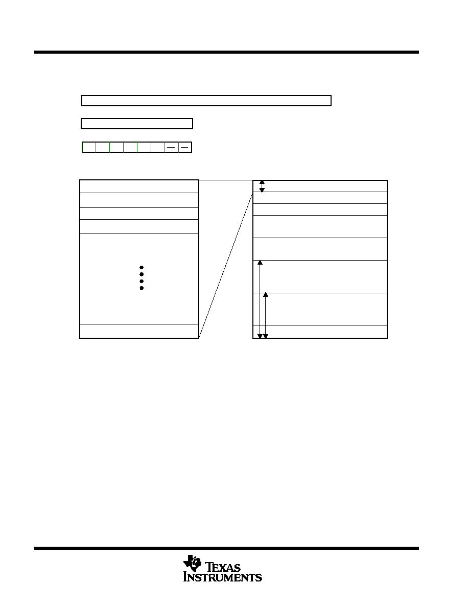
5
6
7
8
9
10
11
3 2 1 28 27
12 13
25
24
23
22
21
20
19
AN3
AN2
AN1
AN0
SCITXD
SCIRXD
MC
XTAL2 / CLKIN
XTAL1
A6
A5
A4
A3
A2
4
26
14 15 16 1718
A1
A0
INT1
T1EVT
T1PWM
T1IC
/
C
R
A7
D6
D3
/
SYSCLK
V
V
RESET
D4
FZ AND FN PACKAGES
( TOP VIEW )
D7
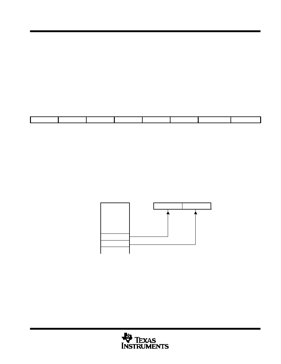
1
2
3
4
5
6
7
8
9
10
11
12
13
14
28
27
26
25
24
23
22
21
20
19
18
17
16
15
VCC
D3 / SYSCLK
D6
A7
XTAL2 / CLKIN
XTAL1
A6
A5
A4
A3
A2
D7
A1
A0
VSS
RESET
D4
AN3
AN2
AN1
AN0
SCITXD
SCIRXD
MC
T1IC / CR
T1PWM
T1EVT
INT1
JD AND N PACKAGES
( TOP VIEW )
CC
SS
PRODUCTION DATA information is current as of publication date.
Products conform to specifications per the terms of Texas Instruments
standard warranty. Production processing does not necessarily include
testing of all parameters.
Copyright
©
1997, Texas Instruments Incorporated
TMS370CxCx
8-BIT MICROCONTROLLER
SPNS040B ≠ NOVEMBER 1995 ≠ REVISED FEBRUARY 1997
2
POST OFFICE BOX 1443
∑
HOUSTON, TEXAS 77251≠1443
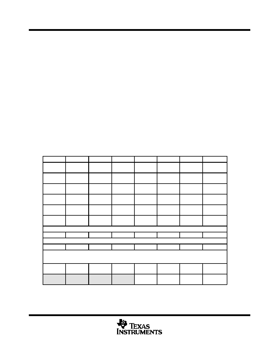
Pin Descriptions
28 PINS
DIP and LCC
I / O
DESCRIPTION
NAME
NO.
A0
A1
A2
A3
A4
A5
A6
A7
14
13
11
10
9
8
7
4
I / O
Port A is a general-purpose bidirectional I / O port.
D3/SYSCLK
D4
D6
D7
2
26
3
12
I / O
Port D is a general-purpose bidirectional I / O port. D3 is also configurable as SYSCLK.
INT1
15
I
External interrupt (non-maskable or maskable) / general-purpose input pin.
AN0 /E0
AN1 / E1
AN2 / E2
AN3 / E3
22
23
24
25
I
ADC2 module analog input (AN0 ≠ AN3) or positive reference pins (AN1 ≠ AN3).
Port E can be individually programmed as general-purpose input pins if not used as ADC2 analog input.
T1IC / CR
T1PWM
T1EVT
18
17
16
I / O
Timer1 input capture / counter reset input pin / general-purpose bidirectional pin.
Timer1 PWM output pin / general-purpose bidirectional pin.
Timer1 external event input pin / general-purpose bidirectional pin.
SCITXD
SCIRXD
21
20
I / O
SCI module transmit data output / general-purpose bidirectional pin. (See Note 1)
SCI module receive data input pin / general-purpose bidirectional pin.
RESET
27
I / O
System reset bidirectional pin; as input pin, RESET initializes the microcontroller; as open-drain output,
RESET indicates that an internal failure was detected by watchdog or oscillator fault circuit.
MC
19
I
Mode control input pin; programming EPROM when VPP is applied to MC pin.
XTAL2 / CLKIN
XTAL1
5
6
I
O
Internal oscillator crystal input / External clock source input.
Internal oscillator output for crystal.
VCC
1
Positive supply voltage
VSS
28
Ground reference
I = input, O = output
NOTE 1: The two SCI configuration pins are referenced to as SCI2.
TMS370CxCx
8-BIT MICROCONTROLLER
SPNS040B ≠ NOVEMBER 1995 ≠ REVISED FEBRUARY 1997
3
POST OFFICE BOX 1443
∑
HOUSTON, TEXAS 77251≠1443
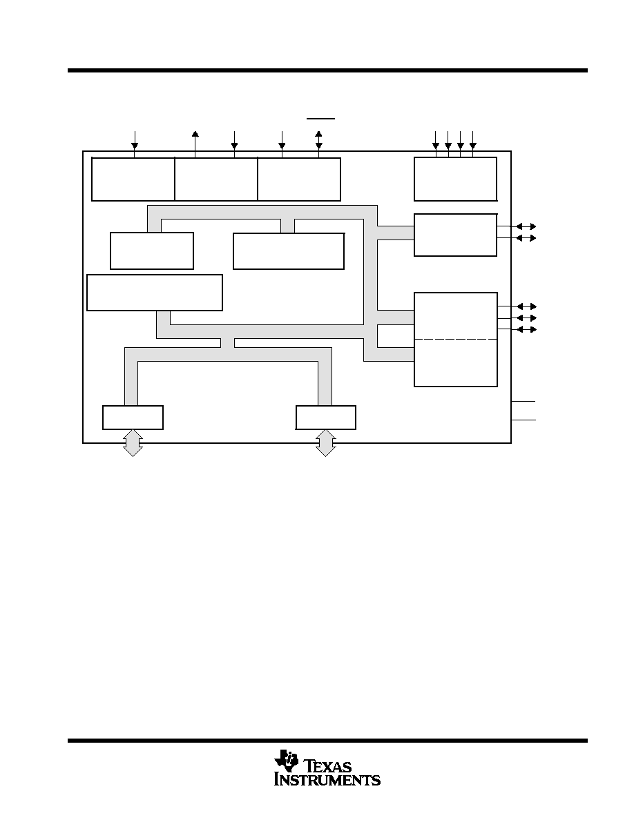
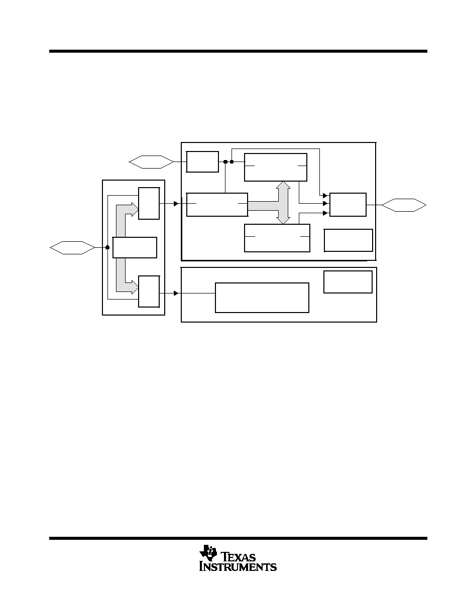
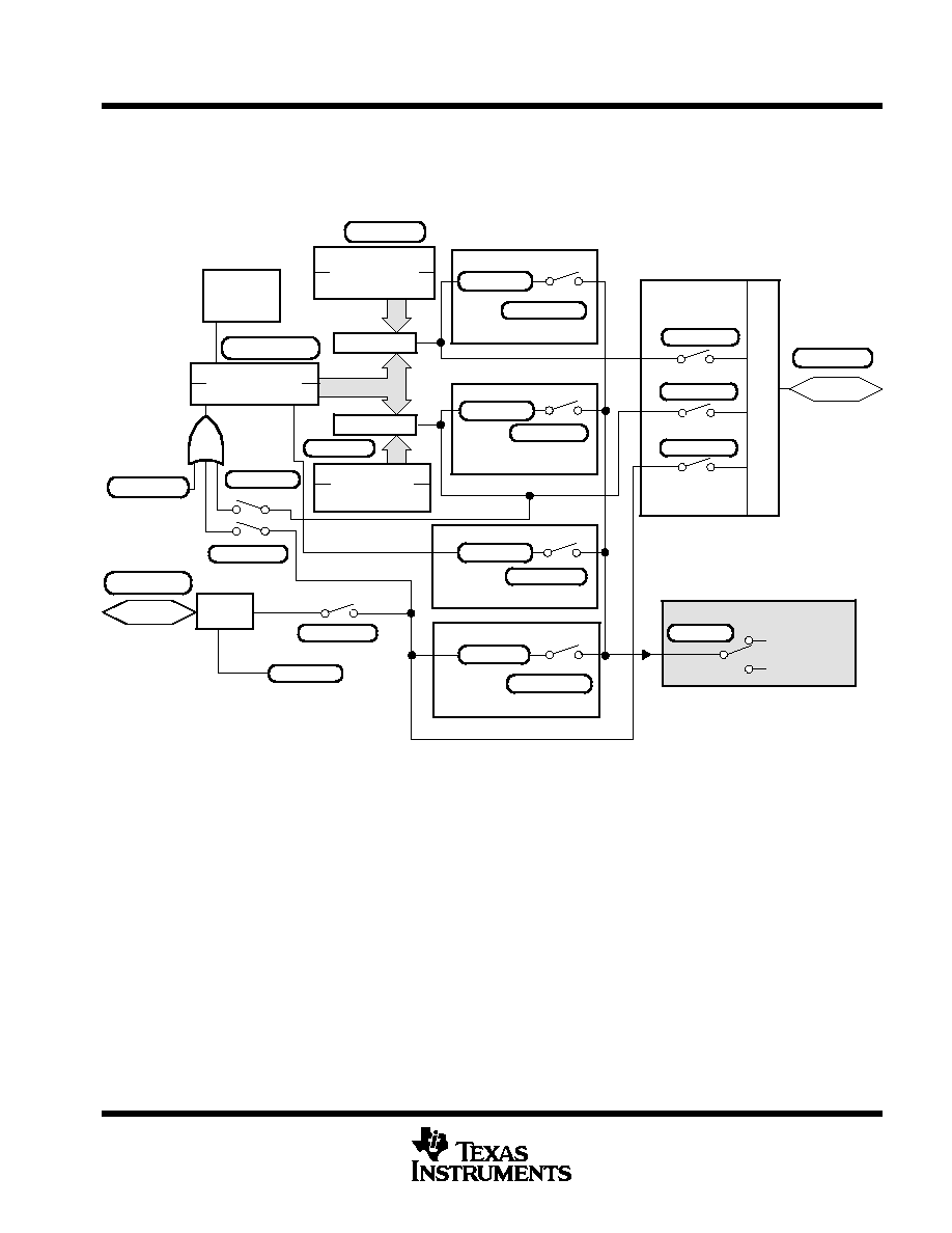
functional block diagram
Interrupts
T1IC/CR
T1EVT
T1PWM
V
System
Control
Clock Options:
Divide-By-4 Or
Divide-By-1 (PLL)
RAM
128 Bytes
CPU
Port A
Port D
Timer 1
Watchdog
INT1
XTAL1
XTAL2/
CLKIN
MC
SCIRXD
SCITXD
Serial
Communications
Interface 2
RESET
SS
VCC
Program Memory
ROM: 4K Bytes
EPROM: 8K Bytes
4
A -to-D
Converter 2
E0 ≠ E3
or
AN0 ≠ AN3
8
description
The TMS370C3C0, TMS370C6C2, and SE370C6C2 devices are members of the TMS370 family of single-chip
8-bit microcontrollers. Unless otherwise noted, the term TMS370CxCx refers to these devices. The TMS370
family provides cost-effective real-time system control through integration of advanced peripheral function
modules and various on-chip memory configurations.
The TMS370CxCx family of devices is implemented using high-performance silicon-gate CMOS EPROM
technologies. Low-operating power, wide-operating temperature range, and noise immunity of CMOS
technology coupled with the high performance and extensive on-chip peripheral functions make the
TMS370CxCx devices attractive in system designs for automotive electronics, industrial motors, computer
peripheral controls, telecommunications, and consumer applications.
All TMS370CxCx devices contain the following on-chip peripheral modules:
D
Four-channel, 8-bit analog to digital converter 2 (ADC2)
D
Serial communications interface 2 (SCI2)
D
One 24-bit general-purpose watchdog timer
D
One 16-bit general-purpose timer with an 8-bit prescaler
TMS370CxCx
8-BIT MICROCONTROLLER
SPNS040B ≠ NOVEMBER 1995 ≠ REVISED FEBRUARY 1997
4
POST OFFICE BOX 1443
∑
HOUSTON, TEXAS 77251≠1443
description (continued)
Table 1 provides a memory configuration overview of the TMS370CxCx devices.
Table 1. Memory Configurations
DEVICES
PROGRAM MEMORY
(BYTES)
DATA MEMORY
(BYTES)
PACKAGES
28-PIN LCC OR DIP
ROM
EPROM
RAM
EEPROM
28-PIN LCC OR DIP
TMS370C3C0A
4K
--
128
--
FN ≠ PLCC
N ≠ PDIP
TMS370C6C2A
--
8K
128
--
FN ≠ PLCC
N ≠ PDIP
SE370C6C2A
--
8K
128
--
FZ ≠ CLCC
JD ≠ CDIP
System evaluators and development are for use only in prototype environment, and their reliability has not been characterized.
The suffix letter (A) appended to the device name (shown in Table 1) indicates configuration of the device. ROM
or EPROM devices have different configurations as indicated in Table 2. ROM devices with the suffix letter A
are configured through a programmable contact during manufacture.
Table 2. Suffix Letter Configuration
DEVICE
WATCHDOG TIMER
CLOCK
LOW-POWER MODE
EPROM A
Standard
Divide-by-4 (standard oscillator)
Enabled
Standard
Di id b 4
ROM A
Hard
Divide-by-4 or
Divide-by-1 (PLL)
Enabled or disabled
Simple
Divide-by-1 (PLL)
The 4K bytes of mask-programmable ROM in the associated TMS370C3C0A device are replaced in the
TMS370C6C2A with 8K bytes of EPROM while all other available memory and on-chip peripherals are identical.
The one-time programmable (OTP) (TMS370C6C2A) and reprogrammable (SE370C6C2A) devices are
available.
TMS370C6C2A OTP devices are available in plastic packages. This microcontroller is effective to use for
immediate production updates for other members of the TMS370C3C0A or for low-volume production runs
when the mask charge or cycle time for the low-cost mask ROM devices is not practical.
The SE370C6C2A has a windowed ceramic package to allow reprogramming of the program EPROM memory
during the development-prototyping phase of design. The SE370C6C2A devices allow quick updates to
breadboards and prototype systems during initial design iterations.
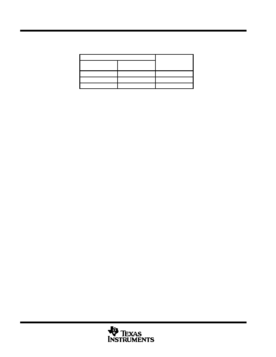
The TMS370CxCx family provides two low-power modes (STANDBY and HALT) for applications where
low-power consumption is critical. Both modes stop all CPU activity, that is, no instructions are executed. In the
STANDBY mode, the internal oscillator and the general-purpose timer remain active. In the HALT mode, all
device activity is stopped. The device retains all RAM data and peripheral configuration bits throughout both
low-power modes.
The TMS370CxCx features advanced register-to-register architecture that allows direct arithmetic and logical
operations without requiring an accumulator (for example, ADD R24, R47; add the contents of register 24 to
the contents of register 47 and store the result in register 47). The TMS370CxCx family is fully instruction-set
compatible, providing easy transition between members of the TMS370 8-bit microcontroller family.

TMS370CxCx
8-BIT MICROCONTROLLER
SPNS040B ≠ NOVEMBER 1995 ≠ REVISED FEBRUARY 1997
5
POST OFFICE BOX 1443
∑
HOUSTON, TEXAS 77251≠1443
description (continued)
The TMS370CxCx device has one operational mode of serial communications provided by the SCI2 module.
The SCI2 allows standard RS-232-C communications with other common data transmission equipment.
The TMS370CxCx family provides the system designer with economical, efficient solutions to real-time control
applications. The TMS370 family compact development tool (CDT
TM
) solves the challenge of efficiently
developing the software and hardware required to design the TMS370CxCx into an ever-increasing number of
complex applications. The application source code can be written in assembly and C-language, and the output
code can be generated by the linker. The TMS370 family CDT development tool can communicate through a
standard RS-232-C interface with an existing personal computer. This allows the use of the personal computer
editors and software utilities already familiar to the designer. The TMS370 family CDT emphasizes ease-of-use
through extensive menus and screen windowing so that a system designer can begin developing software with
minimal training. Precise real-time in-circuit emulation and extensive symbolic debug and analysis tools ensure
efficient software and hardware implementation as well as reduced time-to-market cycle.
The TMS370CxCx family together with the TMS370 family CDT370, software tools, the SE370C6C2A
reprogrammable devices, comprehensive product documentation, and customer support provide a complete
solution to the needs of the system designer.
central processing unit (CPU)
The CPU used on the TMS370CxCx device is the high-performance 8-bit TMS370 CPU module. The 'xCx
implements an efficient register-to-register architecture that eliminates the conventional accumulator
bottleneck. The complete 'xCx instruction map is shown in Table 36 in the TMS370CxCx instruction set
overview section.
The '370CxCx CPU architecture provides the following components:
CPU registers:
D
A stack pointer that points to the last entry in the memory stack.
D
A status register that monitors the operation of the instructions and contains the global-interrupt enable bits.
D
A program counter (PC) that points to the memory location of the next instruction to be executed.
CDT is a trademark of Texas Instruments Incorporated.
TMS370CxCx
8-BIT MICROCONTROLLER
SPNS040B ≠ NOVEMBER 1995 ≠ REVISED FEBRUARY 1997
6
POST OFFICE BOX 1443
∑
HOUSTON, TEXAS 77251≠1443
central processing unit (CPU) (continued)
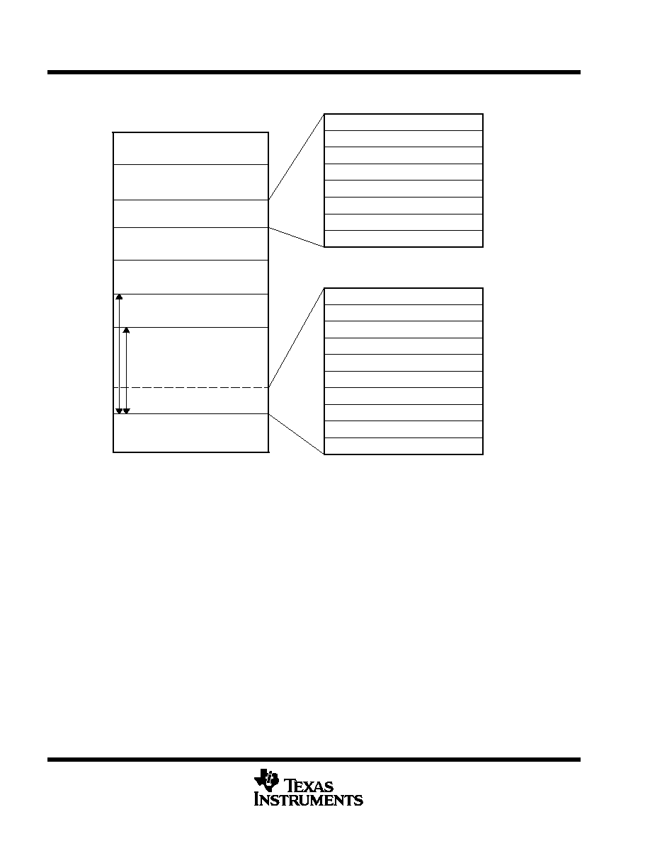
Figure 1 illustrates the CPU registers and memory blocks.
0080h
0FFFh
Reserved
Peripheral File
Not Available
1FFFh
2000h
5FFFh
6000h
Interrupts and Reset Vectors;
Trap Vectors
107Fh
1080h
Reserved
7FFFh
0
RAM (Includes up to 256-Byte Registers File)
0
15
Program Counter
7
Legend:
Z=Zero
IE1=Level 1 interrupts Enable
C=Carry
V=Overflow
N=Negative
IE2=Level 2 interrupts Enable
IE1
IE2
Z
N
C
0
1
2
3
4
5
6
7
V
Status Register (ST)
Stack Pointer (SP)
R0(A)
R1(B)
R3
0000h
0001h
0002h
R127
0003h
R2
007Fh
6FFFh
7000h
8K-Byte EPROM (6000h ≠ 7FFFh)
4K-Byte ROM (7000h ≠ 7FFFh)
7FC0h
7FBFh
128-Byte RAM (0000h≠007Fh)
007Fh
1000h
0000h
Reserved means the address space is reserved for future expansion.
Not available means the address space is not accessible.
Figure 1. Programmer's Model
A memory map that includes:
D
128-byte general-purpose RAM that can be used for data memory storage, program instructions,
general-purpose register, or the stack
D
A peripheral file that provides access to all internal peripheral modules, system-wide control functions and
EPROM programming control
D
4K-byte ROM or 8K-byte EPROM program memory
stack pointer (SP)
The SP is an 8-bit CPU register that operates as a last-in, first-out, read / write memory. Typically, the stack is
used to store the return address on subroutine calls as well as the status-register contents during interrupt
sequences.
The SP points to the last entry or top of the stack. The SP is incremented automatically before data is pushed
onto the stack and decremented after data is popped from the stack. The stack can be placed anywhere in the
on-chip RAM.
TMS370CxCx
8-BIT MICROCONTROLLER
SPNS040B ≠ NOVEMBER 1995 ≠ REVISED FEBRUARY 1997
7
POST OFFICE BOX 1443
∑
HOUSTON, TEXAS 77251≠1443
central processing unit (CPU) (continued)
status register (ST)
The ST monitors the operation of the instructions and contains the global interrupt-enable bits. The ST register
includes four status bits (condition flags) and two interrupt-enable bits:
D
The four status bits indicate the outcome of the previous instruction; conditional instructions (for example,
the conditional jump instructions) use the status bits to determine program flow.
D
The two interrupt-enable bits control the two interrupt levels.
The ST register, status-bit notation, and status-bit definitions are shown in Table 3.
Table 3. Status Register (ST)
7
6
5
4
3
2
1
0
C
N
Z
V
IE2
IE1
Reserved
Reserved
RW-0
RW-0
RW-0
RW-0
RW-0
RW-0
R = read, W = write, 0 = value after reset
program counter (PC)
The contents of the PC point to the memory location of the next instruction to be executed. The PC consists
of two 8-bit registers in the CPU: the program counter high (PCH) and program counter low (PCL). These
registers contain the most significant byte (MSbyte) and least significant byte (LSbyte) of a 16-bit address.
During reset, the contents of the reset vector (7FFEh, 7FFFh) are loaded into the program counter. The PCH
(MSbyte of the PC) is loaded with the contents of memory location 7FFEh, and the PCL (LSbyte of the PC) is
loaded with the contents of memory location 7FFFh. Figure 2 shows this operation using an example value of
7000h as the contents of the reset vector.
Memory
Program Counter (PC)
70
00
PCH
PCL
70
00
0000h
7FFEh
7FFFh
Figure 2. Program Counter After Reset
memory map
The TMS370CxCx architecture is based on the Von Neuman architecture, where the program memory and data
memory share a common address space. All peripheral input / output is memory mapped in this same common
address space. As shown in Figure 3, the TMS370CxCx provides memory-mapped RAM, ROM, input / output
pins, peripheral functions, and system interrupt vectors.
The peripheral file contains all input / output port control, peripheral status and control, EPROM, and
system-wide control functions. The peripheral file is located from 1000h to 107Fh and is logically divided into
seven peripheral file frames of 16 bytes each. Each on-chip peripheral is assigned to a separate frame through
which peripheral control and data information is passed.
TMS370CxCx
8-BIT MICROCONTROLLER
SPNS040B ≠ NOVEMBER 1995 ≠ REVISED FEBRUARY 1997
8
POST OFFICE BOX 1443
∑
HOUSTON, TEXAS 77251≠1443
memory map (continued)
128-Byte RAM
(Register File / Stack)
Peripheral File
Reserved
Not Available
Reserved
System Control
Digital Port Control
Timer 1 Peripheral Control
Vectors
Not Available
Reserved
0000h
0080h
007Fh
1000h
107Fh
1080h
1FFFh
2000h
5FFFh
6000h
6FFFh
7000h
FFFFh
0FFFh
4K-Byte ROM
(7000h ≠ 7FFFh)
Interrupts and Reset Vectors;
Trap Vectors
7FBFh
7FC0h
7FFFh
8000h
Peripheral File Control Registers
8K-Byte EPROM
(6000h ≠ 7FFFh)
1010h ≠ 101Fh
1020h ≠ 102Fh
1040h ≠ 104Fh
1030h ≠ 103Fh
SCI2 Peripheral Control
1050h ≠ 105Fh
Trap 15 ≠ 0
7FC0h ≠ 7FDFh
Reserved
7FE0h ≠ 7FEBh
Analog-To-Digital Converter 2
7FECh ≠ 7FEDh
Reserved
7FEEh ≠ 7FEFh
SCI TX
7FF0h ≠ 7FF1h
SCI RX
7FF2h ≠ 7FF3h
Timer 1
7FF4h ≠ 7FF5h
Reserved
7FF6h ≠ 7FFBh
Interrupt 1
7FFCh ≠ 7FFDh
Reset
7FFEh ≠ 7FFFh
Reserved
1000h ≠ 100Fh
Reserved
1060h ≠ 106Fh
ADC2 Peripheral Control
1070h ≠ 107Fh
Reserved means the address space is reserved for future expansion.
Not available means the address space is not accessible.
Figure 3. TMS370CxCx Memory Map
RAM / register file (RF)
Locations within the RAM address space can serve as the RF, general-purpose read / write memory, program
memory, or the stack instructions. The TMS370CxCx devices contain 128 bytes of internal RAM mapped
beginning at location 0000h (R0) and continuing through location 007Fh (R127) which is shown in Figure 1.
The first two registers, R0 and R1, are also called register A and B, respectively. Some instructions implicitly
use register A or B; for example, the instruction LDSP (load SP) assumes that the value to be loaded into the
SP is contained in register B. Registers A and B are the only registers cleared on reset.
peripheral file (PF)
The TMS370CxCx control registers contain all the registers necessary to operate the system and peripheral
modules on the device. The instruction set includes some instructions that access the PF directly. These
instructions designate the register by the number of the PF relative to 1000h, preceded by P0 for a hexadecimal
designator or P for a decimal designator. For example, the system control register 0 (SCCR0) is located at
address 1010h; its peripheral file hexadecimal designator is P010, and its decimal designator is P16. Table 4
shows the TMS370CxCx PF address map.
TMS370CxCx
8-BIT MICROCONTROLLER
SPNS040B ≠ NOVEMBER 1995 ≠ REVISED FEBRUARY 1997
9
POST OFFICE BOX 1443
∑
HOUSTON, TEXAS 77251≠1443
peripheral file (PF) (continued)
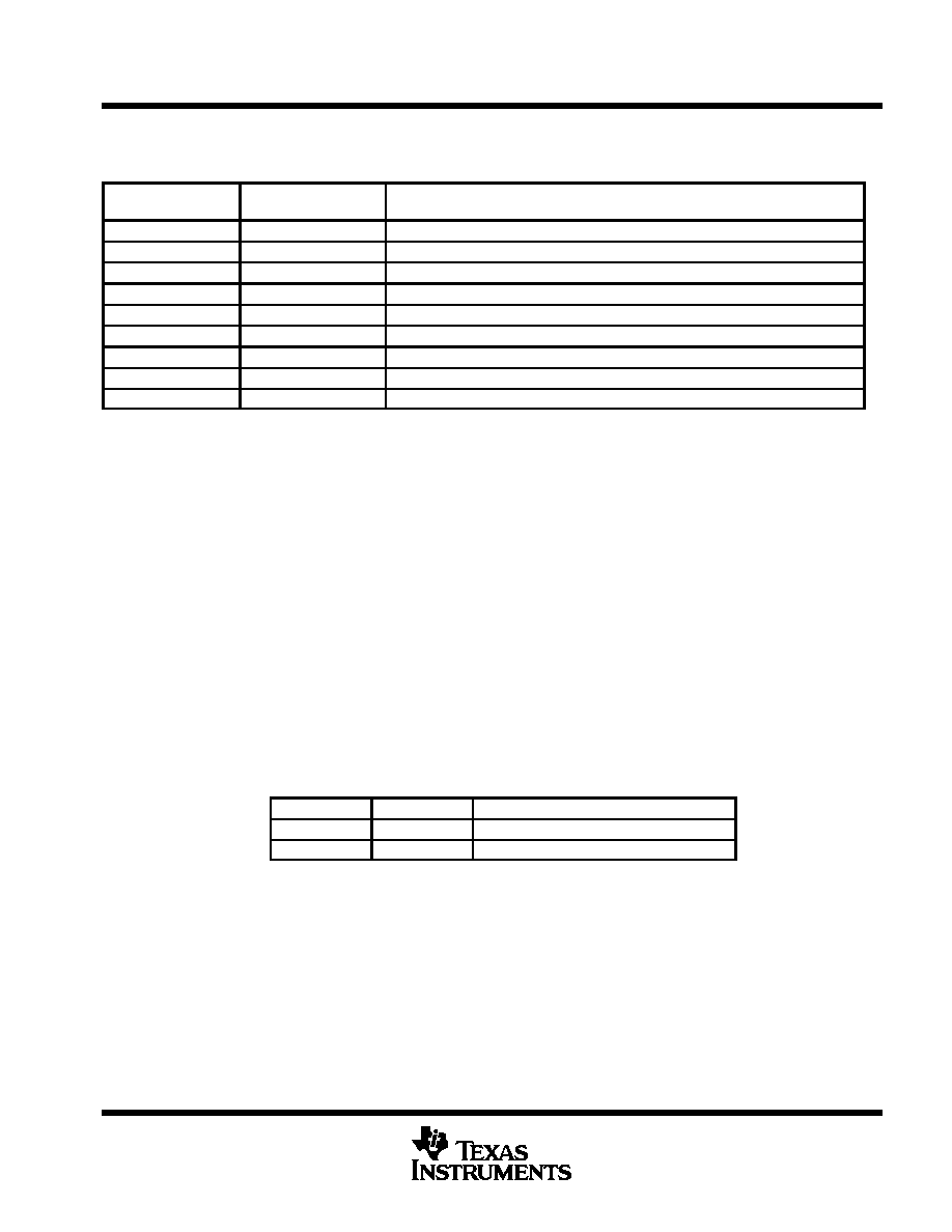
Table 4. TMS370CxCx Peripheral File Address Map
ADDRESS RANGE
PERIPHERAL FILE
DESIGNATOR
DESCRIPTION
1000h ≠ 100Fh
P000 ≠ P00F
Reserved
1010h ≠ 101Fh
P010 ≠ P01F
System and EPROM control registers
1020h ≠ 102Fh
P020 ≠ P02F
Digital I / O port control registers
1030h ≠ 103Fh
P030 ≠ P03F
Reserved
1040h ≠ 104Fh
P040 ≠ P04F
Timer 1 registers
1050h ≠ 105Fh
P050 ≠ P05F
Serial communications interface 2 registers
1060h ≠ 106Fh
P060 ≠ P06F
Reserved
1070h ≠ 107Fh
P070 ≠ P07F
Analog-to-digital converter 2 registers
1080h ≠ 1FFFh
P080 ≠ P0FF
Reserved
program EPROM
The TMS370C6C2 device contains 8K bytes of EPROM mapped at location 6000h and continuing through
location 7FFFh as shown in Figure 3. Reading the program EPROM modules is identical to reading other
internal memory. During programming, the EPROM is controlled by the EPROM control register (EPCTL). The
program EPROM module features include:
D
Programming
≠
In-circuit programming capability if V
PP
is applied to MC
≠
Control register: EPROM programming is controlled by the EPROM control register (EPCTL) located in
the peripheral file (PF) frame at location P01Ch as shown in Table 5.
D
Write protection: Writes to the program EPROM are disabled under the following conditions:
≠
Reset halts all programming to the EPROM module.
≠
Low-power modes
≠
13 V not applied to MC
Table 5. Data EEPROM and Program EPROM Control Registers Memory Map
¡¡¡¡¡
¡¡¡¡¡
ADDRESS
¡¡¡¡¡
¡¡¡¡¡
SYMBOL
¡¡¡¡¡¡¡¡¡¡¡¡
¡¡¡¡¡¡¡¡¡¡¡¡
NAME
¡¡¡¡¡
¡¡¡¡¡
P01A to P01B
¡¡¡¡¡
¡¡¡¡¡
--
¡¡¡¡¡¡¡¡¡¡¡¡
¡¡¡¡¡¡¡¡¡¡¡¡
Reserved
¡¡¡¡¡
¡¡¡¡¡
P01C
¡¡¡¡¡
¡¡¡¡¡
EPCTL
¡¡¡¡¡¡¡¡¡¡¡¡
¡¡¡¡¡¡¡¡¡¡¡¡
Program EPROM Control Register
program ROM
The program read-only memory (ROM) consists of 4K bytes of mask-programmable ROM. The program ROM
is used for permanent storage of data or instructions. Programming of the mask ROM is performed at the time
of device fabrication. Refer to Figure 3 for ROM memory map.
Memory addresses 7FE0h through 7FEBh are reserved for Texas Instruments, and addresses 7FECh through 7FFFh are reserved for
interrupt and reset vectors. Trap vectors, used with TRAP0 through TRAP15 instructions, are located between addresses 7FC0h and
7FDFh.
TMS370CxCx
8-BIT MICROCONTROLLER
SPNS040B ≠ NOVEMBER 1995 ≠ REVISED FEBRUARY 1997
10
POST OFFICE BOX 1443
∑
HOUSTON, TEXAS 77251≠1443
system reset
The system reset operation ensures an orderly start-up sequence for the TMS370CxCx CPU-based device.
There are up to three different actions that can cause a system reset to the device. Two of these actions are
internally generated, while one (RESET pin) is controlled externally. These actions are as follows:
D
External RESET pin. A low level signal can trigger an external reset. To ensure a reset, the external signal
should be held low for one SYSCLK cycle. Signals of less than one SYSCLK can generate a reset. See the
TMS370 User's Guide (literature number SPNU127) for more information.
D
Watchdog (WD) timer. A watchdog-generated reset occurs if an improper value is written to the WD key
register, or if the re-initialization does not occur before the watchdog timer timeout . See the
TMS370 User's
Guide (literature number SPNU127) for more information.
D
Oscillator reset. Reset occurs when the oscillator operates outside of the recommended operating range.
See the
TMS370 User's Guide (literature number SPNU127) for more information.
Once a reset source is activated, the external RESET pin is driven low (active) for a minimum of eight SYSCLK
cycles. This allows the 'xCx device to reset external system components. Additionally, if a cold start (V
CC
is off
for several hundred milliseconds) condition or oscillator failure occurs or the RESET pin is held low, then the
reset logic holds the device in a reset state for as long as these actions are active.
After a reset, the program can check the oscillator fault flag (OSC FLT FLAG, SCCR0.4), the cold start flag
(COLD START, SCCR0.7) and the watchdog reset (WD OVRFL INT FLAG, T1CTL2.5) to determine the source
of the reset. A reset does not clear these flags. Table 6 lists the reset sources.
Table 6. Reset Sources
REGISTER
ADDRESS
PF
BIT NO.
CONTROL BIT
SOURCE OF RESET
SCCR0
1010h
P010
7
COLD START
Cold (power-up)
SCCR0
1010h
P010
4
OSC FLT FLAG
Oscillator out of range
T1CTL2
104Ah
P04A
5
WD OVRFL INT FLAG
Watchdog timer timeout
Once a reset is activated, the following sequence of events occurs:
1.
CPU registers are initialized: ST = 00h, SP = 01h (reset state).
2.
Registers A and B are initialized to 00h (no other RAM is changed).
3.
The contents of the LSbyte of the reset vector (07FFh) are read and stored in the PCL.
4.
The contents of the MSbyte of the reset vector (07FEh) are read and stored in the PCH.
5.
Program execution begins with an opcode fetch from the address pointed to the PC.
The reset sequence takes 20 SYSCLK cycles from the time the reset pulse is released until the first opcode
fetch. During a reset, RAM contents (except for registers A and B) remain unchanged, and the module control
register bits are initialized to their reset state.
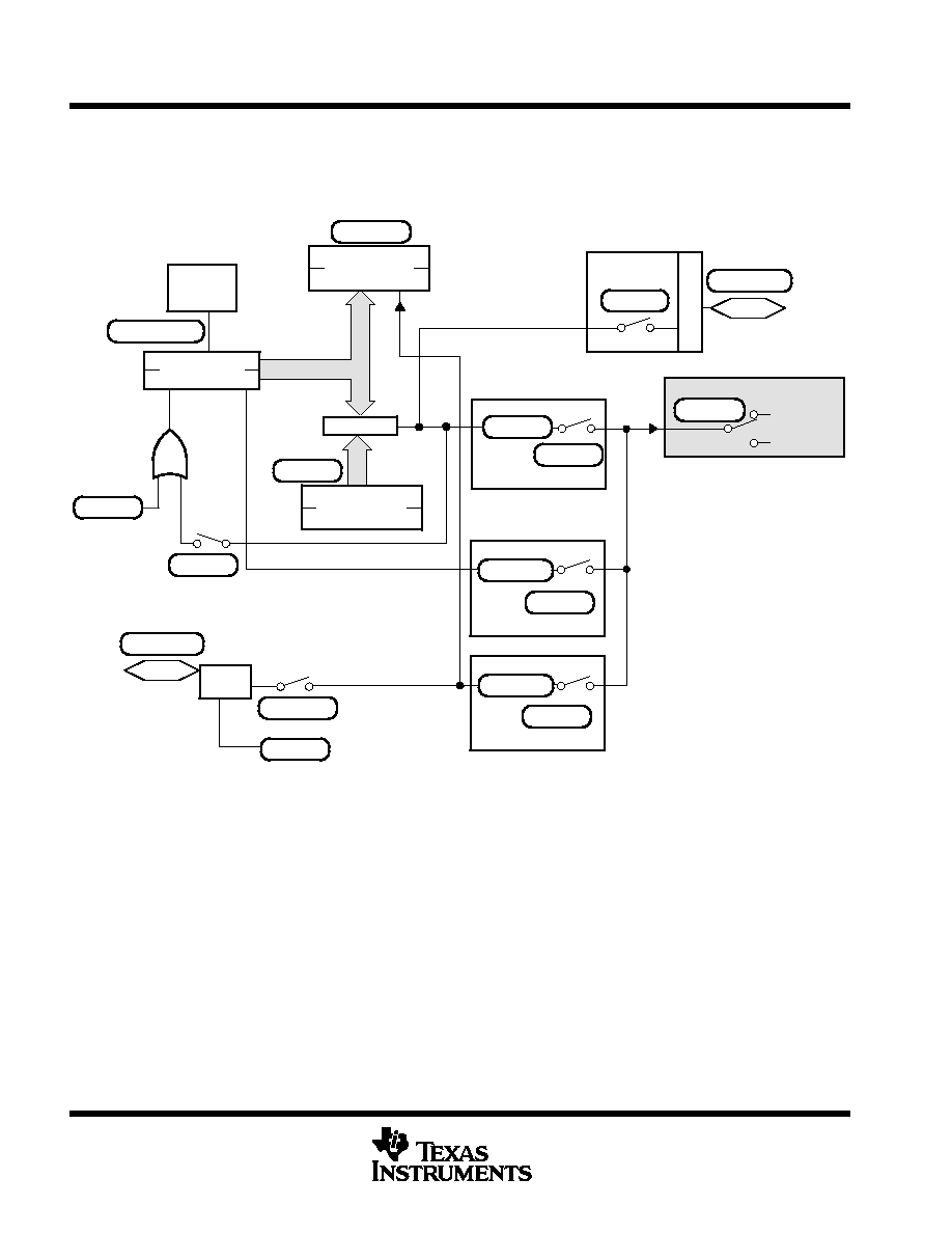
interrupts
The TMS370 family software programmable interrupt structure permits flexible on-chip and external interrupt
configurations to meet real-time interrupt-driven application requirements. The hardware interrupt structure
incorporates two priority levels as shown in Figure 4. Interrupt level 1 has a higher priority than interrupt
level 2. The two priority levels can be masked independently by the global-interrupt mask bits (IE1 and IE2) of
the status register.
TMS370CxCx
8-BIT MICROCONTROLLER
SPNS040B ≠ NOVEMBER 1995 ≠ REVISED FEBRUARY 1997
11
POST OFFICE BOX 1443
∑
HOUSTON, TEXAS 77251≠1443
interrupts (continued)
TIMER 1
CPU
NMI
Logic
Enable
IE1
IE2
Level 1 INT
Level 2 INT
T1 PRI
Priority
Overflow
Compare 1
Ext Edge
Compare 2
Input Capture 1
Watchdog
ADC2 INT
A / D PRI
A / D
STATUS REG
EXT INT 1
INT1 PRI
INT1
SCI2 INT
RX
BRKDT
RXRDY
TX
TXRDY
TXPRI
RXPRI
Figure 4. Interrupt Control
Each system interrupt is configured independently to either the high- or low-priority chain by the application
program during system initialization. Within each interrupt chain, the interrupt priority is fixed by the position of
the system interrupt. However, since each system interrupt is selectively configured on either the high- or
low-priority interrupt chain, the application program can elevate any system interrupt to the highest priority.
Arbitration between the two priority levels is performed within the CPU. Arbitration within each of the priority
chains is performed within the peripheral modules to support interrupt expansion for future modules.
Pending-interrupts are serviced upon completion of current instruction execution, depending on their interrupt
mask and priority conditions.
The TMS370CxCx has five hardware system interrupts (plus RESET) as shown in Table 7. Each system
interrupt has a dedicated vector located in program memory through which control is passed to the interrupt
service routines. A system interrupt may have multiple interrupt sources (for example, SCI RXINT has two
interrupt sources). All of the interrupt sources are individually maskable by local interrupt-enable control bits in
the associated peripheral file. Each interrupt source FLAG bit is readable individually for software polling or for
determining which interrupt source generated the associated system interrupt.
Four of the system interrupts are generated by on-chip peripheral functions, and one external interrupt is
supported. Software configuration of the external interrupts is performed through the INT1 control register in
peripheral file frame 1. Each external interrupt is individually software configurable for input polarity (rising or
falling edge) for ease of system interface. External interrupt INT1 is software configurable as either a maskable
or non-maskable interrupt. When INT1 is configured as non-maskable, it cannot be masked by the individual-
TMS370CxCx
8-BIT MICROCONTROLLER
SPNS040B ≠ NOVEMBER 1995 ≠ REVISED FEBRUARY 1997
12
POST OFFICE BOX 1443
∑
HOUSTON, TEXAS 77251≠1443
interrupts (continued)
or global-enable mask bits. The INT1 NMI bit is protected during non-privileged operation and therefore should
be configured during the initialization sequence following reset. To maximize pin flexibility, external interrupt
INT1 can be software-configured as a general-purpose input pin if the interrupt function is not required.
Table 7. Hardware System Interrupts
INTERRUPT SOURCE
INTERRUPT FLAG
SYSTEM
INTERRUPT
VECTOR
ADDRESS
PRIORITY
External RESET
Watchdog Overflow
Oscillator Fault Detect
COLD START
WD OVRFL INT FLAG
OSC FLT FLAG
RESET
7FFEh, 7FFFh
1
External INT1
INT1 FLAG
INT1
7FFCh, 7FFDh
2
Timer 1 Overflow
Timer 1 Compare 1
Timer 1 Compare 2
Timer 1 External Edge
Timer 1 Input Capture 1
Watchdog Overflow
T1 OVRFL INT FLAG
T1C1 INT FLAG
T1C2 INT FLAG
T1EDGE INT FLAG
T1IC1 INT FLAG
WD OVRFL INT FLAG
T1INTß
7FF4h, 7FF5h
3
SCI RX Data Register Full
SCI RX Break Detect
RXRDY FLAG
BRKDT FLAG
RXINT
7FF2h, 7FF3h
4
SCI TX Data Register Empty
TXRDY FLAG
TXINT
7FF0h, 7FF1h
5
A/D Conversion Complete
AD INT FLAG
ADINT
7FECh, 7FEDh
6
Relative priority within an interrupt level.
Release microcontroller from STANDBY and HALT low-power modes.
ß Release microcontroller from STANDBY low-power mode.
privileged operation and EEPROM write-protection override
The TMS370CxCx family has significant flexibility to enable the designer to software configure the system and
peripherals to meet the requirements of a variety of applications. The non-privileged mode of operation ensures
the integrity of the system configuration, once it is defined for an application. Following a hardware reset, the
TMS370CxCx operates in the privileged mode, where all peripheral file registers have unrestricted read / write
access, and the application program configures the system during the initialization sequence following reset.
As the last step of system initialization, the PRIVILEGE DISABLE bit (SCCR2.0) is set to 1 to enter the
non-privileged mode; thus, disabling write operations to specific configuration control bits within the peripheral
file. Table 8 displays the system configuration bits which are write-protected during the non-privileged mode and
must be configured by software prior to exiting the privileged mode.

TMS370CxCx
8-BIT MICROCONTROLLER
SPNS040B ≠ NOVEMBER 1995 ≠ REVISED FEBRUARY 1997
13
POST OFFICE BOX 1443
∑
HOUSTON, TEXAS 77251≠1443
privileged operation and EEPROM write-protection override (continued)
Table 8. Privilege Bits
REGISTER
CONTROL BIT
NAME
LOCATION
CONTROL BIT
SCCR0
P010.5
P010.6
PF AUTO WAIT
OSC POWER
SCCR1
P011.2
P011.4
MEMORY DISABLE
AUTOWAIT DISABLE
SCCR2
P012.0
P012.1
P012.3
P012.4
P012.6
P012.7
PRIVILEGE DISABLE
INT1 NMI
CPU STEST
BUS STEST
PWRDWN / IDLE
HALT / STANDBY
T1PRI
P04F.6
P04F.7
T1 PRIORITY
TI STEST
SCIPRI
P05F.4
P05F.5
P05F.6
P05F.7
SCI ESPEN
SCIRX PRIORITY
SCITX PRIORITY
SCI STEST
ADPRI
P07F.5
P07F.6
P07F.7
AD ESPEN
AD PRIORITY
AD STEST
The privilege bits are shown in a bold typeface in the peripheral file
frame 1 section.
low-power and IDLE modes
The TMS370CxCx devices have two low-power modes (STANDBY and HALT) and an IDLE mode. For
mask-ROM devices, low-power modes can be disabled permanently through a programmable contact at the
time when the mask is manufactured.
The STANDBY and HALT low-power modes significantly reduce power consumption by reducing or stopping
the activity of the various on-chip peripherals when processing is not required. Each of the low-power modes
is entered by executing the IDLE instruction when the PWRDWN / IDLE bit in SCCR2 has been set to 1. The
HALT / STANDBY bit in SCCR2 controls the low-power mode selection.
In the STANDBY mode (HALT / STANDBY = 0), all CPU activity and most peripheral module activity stops;
however, the oscillator, internal clocks, timer 1, and the receive-start bit detection circuit of the serial
communications interface 2 remain active. System processing is suspended until a qualified interrupt (hardware
RESET, external interrupt on INT1, timer 1 interrupt, or low level in the receive pin of the SCI2) is detected.
In the HALT mode (HALT / STANDBY = 1), the TMS370CxCx is placed in its lowest power-consumption mode.
The oscillator and internal clocks are stopped, causing all internal activity to be halted. System activity is
suspended until a qualified interrupt (hardware RESET, external interrupt on the INT1, or low level on the receive
pin of the serial communications interface 2) is detected. The power-down mode selection bits are summarized
in Table 9.
TMS370CxCx
8-BIT MICROCONTROLLER
SPNS040B ≠ NOVEMBER 1995 ≠ REVISED FEBRUARY 1997
14
POST OFFICE BOX 1443
∑
HOUSTON, TEXAS 77251≠1443
low-power and IDLE modes (continued)
Table 9. Low-Power / Idle Control Bits
POWER-DOWN CONTROL BITS
PWRDWN / IDLE
(SCCR2.6)
HALT / STANDBY
(SCCR2.7)
MODE SELECTED
1
0
STANDBY
1
1
HALT
0
X
IDLE
Don't care
When low-power modes are disabled through a programmable contact in the mask-ROM devices, writing to the
SCCR2.6-7 bits are ignored. In addition, if an idle instruction executes when low-power modes are disabled
through a programmable contact, the device always enters the IDLE mode.
To provide a method of always exiting low-power modes for mask-ROM devices, INT1 is enabled automatically
as a nonmaskable interrupt (NMI) during low-power modes when the hard watchdog mode is selected. This
means that the NMI always is generated, regardless of the interrupt enable flags.
The following information is preserved throughout both the STANDBY and HALT modes: RAM (register file),
CPU registers (stack pointer, program counter, and status register), I / O pin direction and output data, and status
registers of all on-chip peripheral functions. Since all CPU instruction processing stops during the STANDBY
and HALT modes, the clocking of the watchdog timer is inhibited.
clock modules
The 'xCx family provides two clock options that are referred to as divide-by-1 (phase-locked loop) and
divide-by-4 (standard oscillator). Both the divide-by-1 and divide-by-4 options are configurable during the
manufacturing process of a TMS370 microcontroller. The 'xCx ROM-masked devices offer both options to meet
system engineering requirements. Only one of the two clock options is allowed on each ROM device. The '6C2A
EPROM has only the divide-by-4.
The divide-by-1 clock module option provides the capability for reduced electromagnetic interference (EMI) with
no added cost.
The divide-by-1 clock module option provides a one-to-one match of the external resonator frequency (CLKIN)
to the internal system clock (SYSCLK) frequency, whereas the divide-by-4 option produces a SYSCLK which
is one-fourth of the frequency of the external resonator. Inside of the divide-by-1 module, the frequency of the
external resonator is multiplied by four, and the clock module then divides the resulting signal by four to provide
the four-phased internal system clock signals. The resulting SYSCLK is equal to the resonator frequency.
TMS370CxCx
8-BIT MICROCONTROLLER
SPNS040B ≠ NOVEMBER 1995 ≠ REVISED FEBRUARY 1997
15
POST OFFICE BOX 1443
∑
HOUSTON, TEXAS 77251≠1443
clock modules (continued)
These are formulated as follows:
Divide-by-4 : SYSCLK
+
external resonator frequency
4
+
CLKIN
4
Divide-by-1 : SYSCLK
+
external resonator frequency
4
4
+
CLKIN
The main advantage of choosing a divide-by-1 oscillator is to reduce EMI. The harmonics of low-speed
resonators extend through less of the emissions spectrum than the harmonics of faster resonators. The
divide-by-1 option provides the capability of reducing the resonator speed by four times, resulting in a steeper
decay of emissions produced by the oscillator.
system configuration registers
Table 10 contains system configuration and control functions. The privileged bits are shown in bold typeface
and shaded areas.
Table 10. System Configuration Registers
PF
BIT 7
BIT 6
BIT 5
BIT 4
BIT 3
BIT 2
BIT 1
BIT 0
REG
P010
COLD
START
OSC
POWER
PF AUTO
WAIT
OSC FLT
FLAG
MC PIN
WPO
MC PIN
DATA
--
µ
P /
µ
C
MODE
SCCR0
P011
--
--
--
AUTO
WAIT
DISABLE
--
MEMORY
DISABLE
--
--
SCCR1
P012
HALT /
STANDBY
PWRDWN /
IDLE
--
BUS
STEST
CPU
STEST
--
INT1
NMI
PRIVILEGE
DISABLE
SCCR2
P013
to
P016
RESERVED
P017
INT1
FLAG
INT1
PIN DATA
--
--
--
INT1
POLARITY
INT1
PRIORITY
INT1
ENABLE
INT1
P018
to
P01B
RESERVED
P01C
BUSY
VPPS
--
--
--
--
W0
EXE
EPCTL
P01D
P01E
P01F
RESERVED
TMS370CxCx
8-BIT MICROCONTROLLER
SPNS040B ≠ NOVEMBER 1995 ≠ REVISED FEBRUARY 1997
16
POST OFFICE BOX 1443
∑
HOUSTON, TEXAS 77251≠1443
digital I / O port configuration registers
Peripheral file frame 2 contains the digital I/O pin configuration and control registers. Table 11 shows the specific
addresses, registers, and control bits within this peripheral file frame. Table 12 shows the port-configuration
register setup.
Table 11. Peripheral File Frame 2: Digital Port-Control Registers
PF
BIT 7
BIT 6
BIT 5
BIT 4
BIT 3
BIT 2
BIT 1
BIT 0
P020
Reserved
APORT1
P021
Port A Control Register 2 (must be 0)
APORT2
P022
Port A Data
ADATA
P023
Port A Direction
ADIR
P024
to
P02B
Reserved
P02C
Port D Control Register 1
(must be 0)
--
Port D Control Register 1
(must be 0)
--
--
--
DPORT1
P02D
Port D Control Register 2
(must be 0)
--
Port D Control Register 2
(must be 0)
--
--
--
DPORT2
P02E
Port D Data
--
Port D Data
--
--
--
DDATA
P02F
Port D Direction
--
Port D Direction
--
--
--
DDIR
To configure pin D3 as SYSCLK, set port D control register 2 = 08h.
Table 12. Port Configuration Register Set-up
PORT
PIN
abcd
00q1
abcd
00y0
A
0 ≠ 7
Data Out q
Data In y
D
3, 4, 6, 7
Data Out q
Data In y
a = Port x Control Register 1
b = Port x Control Register 2
c = Data
d = Direction
TMS370CxCx
8-BIT MICROCONTROLLER
SPNS040B ≠ NOVEMBER 1995 ≠ REVISED FEBRUARY 1997
17
POST OFFICE BOX 1443
∑
HOUSTON, TEXAS 77251≠1443
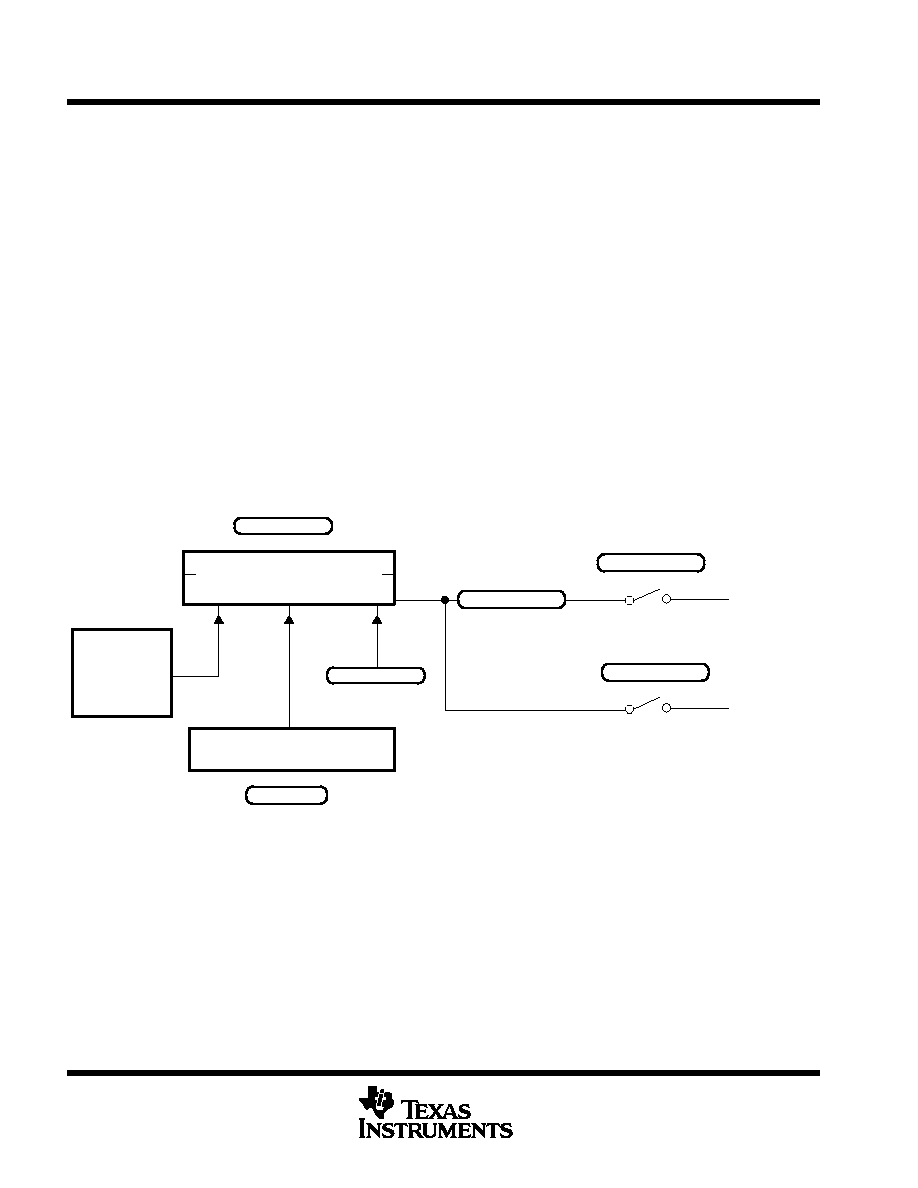
programmable timer 1
The programmable Timer 1 (T1) module of the TMS370CxCx provides the designer with the enhanced timer
resources required to perform real-time system control. The T1 module contains the general-purpose timer and
the watchdog (WD) timer. The two independent 16-bit timers allow program selection of input clock sources
(real-time, external event, or pulse accumulate) with multiple 16-bit registers (input capture and compare) for
special timer function control. The T1 module includes three external device pins that can be used for multiple
counter functions (operation mode dependent) or used as general-purpose I/O pins. The T1 module is shown
in Figure 5.
T1IC/CR
Edge
Select
16-Bit
Counter
T1EVT
MUX
MUX
16-Bit
Register
T1PWM
PWM
Toggle
16
16-Bit
Watchdog Counter
(Aux. Timer)
Interrupt
Logic
Capt/Comp
16-Bit
Register
Compare
Interrupt
Logic
8-Bit
Prescaler
Figure 5. Timer 1 Block Diagram
D
Three T1 I/O pins
≠
T1IC/CR: Timer 1 input capture / counter reset input pin, or general-purpose bidirectional I/O pin
≠
T1PWM: Timer 1 pulse-width-modulation (PWM) output pin, or general-purpose bidirectional I/O pin
≠
T1EVT: Timer 1 event input pin, or general-purpose bidirectional I/O pin
D
Two operation modes:
≠
Dual-compare mode: Provides PWM signal
≠
Capture/compare mode: Provides input capture pin
D
One 16-bit general-purpose resettable counter
D
One 16-bit compare register with associated compare logic
D
One 16-bit capture/compare register, which, depending on the mode of operation, operates as either a
capture or compare register.
D
One 16-bit watchdog counter can be used as an event counter, a pulse accumulator, or an interval timer
if watchdog feature is not needed.
D
Prescaler/clock sources that determine one of eight clock sources for general-purpose timer

TMS370CxCx
8-BIT MICROCONTROLLER
SPNS040B ≠ NOVEMBER 1995 ≠ REVISED FEBRUARY 1997
18
POST OFFICE BOX 1443
∑
HOUSTON, TEXAS 77251≠1443
programmable timer 1 (continued)
D
Selectable edge-detection circuitry that, depending on the mode of operation, senses active transitions on
the input capture pins (T1IC/CR)
D
Interrupts that can be generated on the occurrence of:
≠
A capture
≠
A compare equal
≠
A counter overflow
≠
An external edge detection
D
Sixteen T1 module control registers located in the PF frame beginning at address P040.

TMS370CxCx
8-BIT MICROCONTROLLER
SPNS040B ≠ NOVEMBER 1995 ≠ REVISED FEBRUARY 1997
19
POST OFFICE BOX 1443
∑
HOUSTON, TEXAS 77251≠1443
programmable timer 1 (continued)
The T1 module control registers are listed in Table 13. Privilege bits are shown in bold typeface and shaded.
Table 13. Timer Module Register Memory Map
PF
BIT 7
BIT 6
BIT 5
BIT 4
BIT 3
BIT 2
BIT 1
BIT 0
REG
Mode: Dual-Compare and Capture/Compare
P040
Bit 15
T1Counter MSbyte
Bit 8
T1CNTR
P041
Bit 7
T1 Counter LSbyte
Bit 0
P042
Bit 15
Compare Register MSbyte
Bit 8
T1C
P043
Bit 7
Compare Register LSbyte
Bit 0
P044
Bit 15
Capture/Compare Register MSbyte
Bit 8
T1CC
P045
Bit 7
Capture/Compare Register LSbyte
Bit 0
P046
Bit 15
Watchdog Counter MSbyte
Bit 8
WDCNTR
P047
Bit 7
Watchdog Counter LSbyte
Bit 0
P048
Bit 7
Watchdog Reset Key
Bit 0
WDRST
P049
WD OVRFL
TAP SEL
WD INPUT
SELECT2
WD INPUT
SELECT1
WD INPUT
SELECT0
--
T1 INPUT
SELECT2
T1 INPUT
SELECT1
T1 INPUT
SELECT0
T1CTL1
P04A
WD OVRFL
RST ENA
WD OVRFL
INT ENA
WD OVRFL
INT FLAG
T1 OVRFL
INT ENA
T1 OVRFL
INT FLAG
--
--
T1
SW RESET
T1CTL2
Mode: Dual-Compare
P04B
T1EDGE
INT FLAG
T1C2
INT FLAG
T1C1
INT FLAG
--
--
T1EDGE
INT ENA
T1C2
INT ENA
T1C1
INT ENA
T1CTL3
P04C
T1
MODE=0
T1C1
OUT ENA
T1C2
OUT ENA
T1C1
RST ENA
T1CR
OUT ENA
T1EDGE
POLARITY
T1CR
RST ENA
T1EDGE
DET ENA
T1CTL4
Mode: Capture / Compare
P04B
T1EDGE
INT FLAG
--
T1C1
INT FLAG
--
--
T1EDGE
INT ENA
--
T1C1
INT ENA
T1CTL3
P04C
T1
MODE = 1
T1C1
OUT ENA
--
T1C1
RST ENA
--
T1EDGE
POLARITY
--
T1EDGE
DET ENA
T1CTL4
Mode: Dual-Compare and Capture/Compare
P04D
--
--
--
--
T1EVT
DATA IN
T1EVT
DATA OUT
T1EVT
FUNCTION
T1EVT
DATA DIR
T1PC1
P04E
T1PWM
DATA IN
T1PWM
DATA OUT
T1PWM
FUNCTION
T1PWM
DATA DIR
T1IC/CR
DATA IN
T1IC/CR
DATA OUT
T1IC/CR
FUNCTION
T1IC/CR
DATA DIR
T1PC2
P04F
T1 STEST
T1
PRIORITY
--
--
--
--
--
--
T1PRI
Once the WD OVRFL RST ENA bit is set, these bits cannot be changed until a reset; this applies only to the standard
watchdog and to simple counter. In the hard watchdog, these bits can be modified at any time; the WD INPUT SELECT2
bits are ignored.
TMS370CxCx
8-BIT MICROCONTROLLER
SPNS040B ≠ NOVEMBER 1995 ≠ REVISED FEBRUARY 1997
20
POST OFFICE BOX 1443
∑
HOUSTON, TEXAS 77251≠1443
programmable timer 1 (continued)
Figure 6 shows the T1 capture/compare mode block diagram. The annotations on the diagram identify the
register and the bit(s) in the peripheral frame. For example, the actual address of T1CTL2.0 is 104Ah, bit 0, in
the T1CTL2 register.
T1CTL4.2
16
Compare=
Edge
Select
T1IC/CR
T1EDGE POLARITY
T1EDGE DET ENA
Prescale
Clock
Source
16-Bit
Counter
MSB
LSB
T1CNTR.15-0
Reset
T1C1
RST ENA
T1 SW
RESET
T1CTL2.0
T1CTL4.4
T1PC2.3-0
T1CTL4.0
T1EDGE INT FLAG
T1EDGE INT ENA
T1CTL3.7
T1CTL3.2
T1 OVRFL INT FLAG
T1 OVRFL INT ENA
T1CTL2.3
T1CTL2.4
T1C1 INT FLAG
T1C1 INT ENA
T1CTL3.5
T1CTL3.0
T1C1
OUT ENA
T1PWM
T1CTL4.6
T
oggle
T1PC2.7-4
16-Bit
Capt/Comp
MSB
LSB
Register
T1CC.15-0
T1C.15-0
16-Bit
Compare
MSB
LSB
Register
T1 PRIORITY
T1PRI.6
Level 1 Int
Level 2 Int
0
1
Figure 6. Capture/Compare Mode
TMS370CxCx
8-BIT MICROCONTROLLER
SPNS040B ≠ NOVEMBER 1995 ≠ REVISED FEBRUARY 1997
21
POST OFFICE BOX 1443
∑
HOUSTON, TEXAS 77251≠1443
programmable timer 1 (continued)
Figure 7 shows the T1 dual-compare mode block diagram. The annotations on the diagram identify the register
and the bit(s) in the peripheral frame. For example, the actual address of T1CTL2.0 is 104Ah, bit 0, in the
T1CTL2 register.
T1CTL4.1
T1CTL4.4
Prescaler
Clock
Source
16-Bit
Counter
16-Bit
16
Compare=
Compare=
Reset
T1C1
RST ENA
T1 SW
RESET
Edge
Select
T1EDGE DET ENA
Output
Enable
Capt/Comp
Register MSB
LSB
MSB
LSB
T1CR OUT ENA
T1IC/CR
T1EDGE POLARITY
T
oggle
16-Bit
Compare
MSB
LSB
Register
T1CC.15-0
T1C1 INT FLAG
T1CTL3.0
T1CTL3.5
T1C1 INT ENA
T1C2 INT FLAG
T1CTL3.1
T1CTL3.6
T1C2 INT ENA
T1 OVRFL INT FLAG
T1CTL2.4
T1CTL2.3
T1 OVRFL INT ENA
T1EDGE INT FLAG
T1CTL3.2
T1CTL3.7
T1EDGE INT ENA
T1 PRIORITY
T1C2 OUT ENA
T1C1 OUT ENA
T1CTL4.3
T1CTL4.6
T1CTL4.5
T1PWM
T1PC2.7-4
T1PRI.6
T1C.15-0
T1CNTR.15-0
T1CTL2.0
T1CR
RST ENA
T1PC2.3-0
T1CTL4.0
T1CTL4.2
Level 1 Int
Level 2 Int
0
1
Figure 7. Dual-Compare Mode
TMS370CxCx
8-BIT MICROCONTROLLER
SPNS040B ≠ NOVEMBER 1995 ≠ REVISED FEBRUARY 1997
22
POST OFFICE BOX 1443
∑
HOUSTON, TEXAS 77251≠1443
programmable timer 1 (continued)
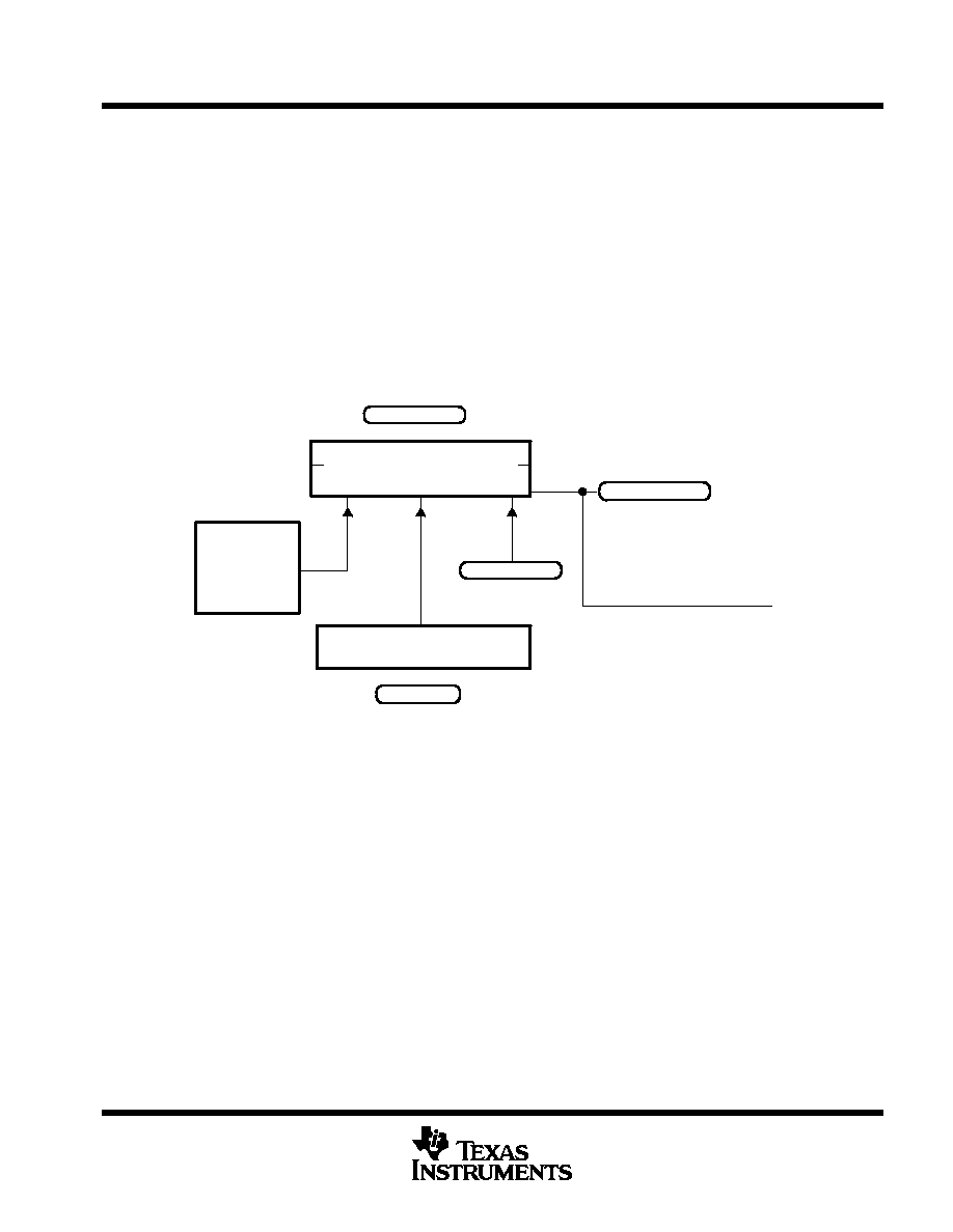
The TMS370CxCx device includes a 24-bit WD timer, contained in the T1 module, which can be programmed
as an event counter, pulse accumulator, or interval timer if the watchdog function is not used. The WD function
is to monitor software and hardware operation and to implement a system reset when the WD counter is not
properly serviced (WD counter overflow or WD counter is re-initialized by an incorrect value). The WD can be
configured as one of the three mask options as follows:
D
Standard watchdog configuration (see Figure 8) ≠ for EPROM and mask-ROM devices:
≠
Watchdog mode
≠
Ten different WD overflow rates ranging from 6.55 ms to 3.35 s at 5 MHz SYSCLK
≠
A WD reset key (WDRST) register is used to clear the watchdog counter (WDCNTR) when a correct
value is written.
≠
Generates a system reset if an incorrect value is written to the watchdog reset key or if the counter
overflows
≠
A watchdog overflow flag (WD OVRFL INT FLAG) bit that indicates whether the WD timer initiated a
system reset
≠
Non-watchdog mode
≠
Watchdog timer can be configured as an event counter, pulse accumulator, or an interval timer.
16-Bit
WatchdogCounter
Reset
Prescaler
Clock
Watchdog Reset Key
WD OVRFL
TAP SEL
WD OVRFL
RST ENA
System Reset
T1CTL1.7
WDRST.7-0
WDCNTR.15-0
T1CTL2.7
T1CTL2.5
WD OVRFL
INT ENA
Interrupt
T1CTL2.6
WD OVRFL
INT FLAG
Figure 8. Standard Watchdog
TMS370CxCx
8-BIT MICROCONTROLLER
SPNS040B ≠ NOVEMBER 1995 ≠ REVISED FEBRUARY 1997
23
POST OFFICE BOX 1443
∑
HOUSTON, TEXAS 77251≠1443
programmable timer 1 (continued)
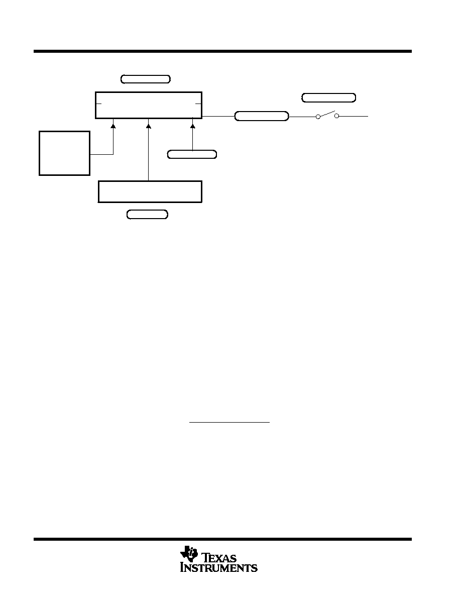
D
Hard watchdog configuration (see Figure 9) ≠ for mask-ROM devices:
≠
Eight different WD overflow rates ranging from 26.2 ms to 3.35 s at 5 MHz SYSCLK
≠
A WD reset key (WDRST) register is used to clear the watchdog counter (WDCNTR) when a correct
value is written.
≠
Generates a system reset if an incorrect value is written to the watchdog reset key or if the counter
overflows.
≠
Automatic activation of the WD timer upon power-up reset
≠
INT1 is enabled as a nonmaskable interrupt during low-power modes.
≠
A watchdog overflow flag (WD OVRFL INT FLAG) bit that indicates whether the WD timer initiated a
system reset
16-Bit
Watchdog Counter
Reset
Prescaler
Clock
Watchdog Reset Key
WD OVRFL
TAP SEL
System Reset
T1CTL1.7
WDRST.7-0
WDCNTR.15-0
T1CTL2.5
WD OVRFL
INT FLAG
Figure 9. Hard Watchdog
D
Simple counter configuration ≠ for mask-ROM devices only (see Figure 10)
≠
Simple counter can be configured as an event counter, pulse accumulator, or an internal timer.
TMS370CxCx
8-BIT MICROCONTROLLER
SPNS040B ≠ NOVEMBER 1995 ≠ REVISED FEBRUARY 1997
24
POST OFFICE BOX 1443
∑
HOUSTON, TEXAS 77251≠1443
programmable timer 1 (continued)
16-Bit
Watchdog Counter
Reset
Prescaler
Clock
Watchdog Reset Key
WD OVRFL
TAP SEL
T1CTL1.7
WDRST.7-0
WDCNTR.15-0
T1CTL2.5
WD OVFL
INT FLAG
WD OVRFL
INT ENA
Interrupt
T1CTL2.6
Figure 10. Simple Counter
serial communications interface 2 module
The TMS370CxCx devices include a serial communications interface 2 (SCI2) module. The SCI2 module
supports digital communications between the TMS370 devices and other asynchronous peripherals and uses
the standard non-return-zero (NRZ) format. The SCI2 modules receiver and transmitter are double buffered,
and each has its own separate enable and interrupt bits. Both can be operated independently or simultaneously
in the full duplex mode. To ensure data integrity, the SCI2 checks received data for break detection, parity,
overrun, and framing errors. The speed of bit rate (baud) is programmable to over 65,000 different speeds
through a 16-bit baud-select register. Features of the SCI2 module include:
D
Two external pins:
≠
SCITXD: SCI2 module transmit-output pin or general-purpose bidirectional I/O pin.
≠
SCIRXD: SCI2 module receive-input pin or general-purpose bidirectional I/O pin.
D
Asynchronous communications mode
D
Baud rate: 64K different programmable rates
≠
Asynchronous mode: 3 bps to 156K bps at 5 MHz SYSCLK
Asynchronous Baud
+
SYSCLK
(BAUD REG
)
1)
32
D
Data word format:
≠
One start bit
≠
Data word length programmable from one to eight bits
≠
Optional even / odd / no parity bit
≠
One or two stop bits
TMS370CxCx
8-BIT MICROCONTROLLER
SPNS040B ≠ NOVEMBER 1995 ≠ REVISED FEBRUARY 1997
25
POST OFFICE BOX 1443
∑
HOUSTON, TEXAS 77251≠1443
serial communications interface 2 module (continued)
D
Four error-detection flags: parity, overrun, framing, and break detection
D
Two wake-up multiprocessor modes: Idle-line and address bit
D
Half or full-duplex operation
D
Double-buffered receiver and transmitter operations
D
Transmitter and receiver operations can be accomplished through either interrupt-driven or
polled-algorithms with status flags:
≠
Transmitter: TXRDY flag (transmitter buffer register is ready to receive another character) and TX
EMPTY flag (Transmitter shift register is empty)
≠
Receiver: RXRDY flag (receive buffer register ready to receive another character), BRKDT flag (break
condition occurred), and RX ERROR monitoring four interrupt conditions
≠
Separate enable bits for transmitter and receiver interrupts
≠
NRZ format
D
Ten SCI2 module control registers located in control register frame beginning at address P050
The SCI2 module control registers are listed in Table 14. Privilege bits are shown in bold typeface and shaded.
Table 14. SCI2 Module Control Register Memory Map
PF
BIT 7
BIT 6
BIT 5
BIT 4
BIT 3
BIT 2
BIT 1
BIT 0
REG
P050
STOP BITS
EVEN/ODD
PARITY
PARITY
ENABLE
ASYNC
ENABLE
ADDRESS/
IDLE WUP
SCI CHAR2
SCI CHAR1
SCI CHAR0
SCICCR
P051
--
--
SCI SW
RESET
CLOCK
ENABLE
TXWAKE
SLEEP
TXENA
RXENA
SCICTL
P052
BAUDF
(MSB)
BAUDE
BAUDD
BAUDC
BAUDB
BAUDA
BAUD9
BAUD8
BAUD MSB
P053
BAUD7
BAUD6
BAUD5
BAUD4
BAUD3
BAUD2
BAUD1
BAUD0
(LSB)
BAUD LSB
P054
TXRDY
TX EMPTY
--
--
--
--
--
SCI TX
INT ENA
TXCTL
P055
RX
ERROR
RXRDY
BRKDT
FE
OE
PE
RXWAKE
SCI RX
INT ENA
RXCTL
P056
RESERVED
P057
RXDT7
RXDT6
RXDT5
RXDT4
RXDT3
RXDT2
RXDT1
RXDT0
RXBUF
P058
RESERVED
P059
TXDT7
TXDT6
TXDT5
TXDT4
TXDT3
TXDT2
TXDT1
TXDT0
TXBUF
P05A
to
P05D
RESERVED
P05E
SCITXD
DATA IN
SCITXD
DATA OUT
SCITXD
FUNCTION
SCITXD
DATA DIR
SCIRXD
DATA IN
SCIRXD
DATA OUT
SCIRXD
FUNCTION
SCIRXD
DATA DIR
SCIPC2
P05F
SCI STEST
SCITX
PRIORITY
SCIRX
PRIORITY
SCI
ESPEN
--
--
--
--
SCIPRI
TMS370CxCx
8-BIT MICROCONTROLLER
SPNS040B ≠ NOVEMBER 1995 ≠ REVISED FEBRUARY 1997
26
POST OFFICE BOX 1443
∑
HOUSTON, TEXAS 77251≠1443
serial communications interface 2 module (continued)
The SCI2 module block diagram is illustrated in Figure 11.
RXCTL.4 ≠ 2
FE OE PE
RX ERROR
SCICTL.3
TXWAKE
SCICCR.6 SCICCR.5
EVEN / ODD ENABLE
PARITY
Frame Format and Mode
WUT
TXBUF.7 ≠ 0
Transmit Data
Buffer Reg.
TXSHF Reg.
TXCTL.7
TXCTL.6
TXRDY
TX EMPTY
SCI TX Interrupt
TXCTL.0
TXENA
8
SCICTL.4
BAUD MSB. 7 ≠ 0
Baud Rate
MSbyte Reg.
BAUD LSB. 7 ≠ 0
Baud Rate
LSbyte Reg.
CLOCK
ENABLE
SCICTL.1
SCITXD
SCI TX INT ENA
RXCTL.7
ERR
RXSHF Reg.
RXCTL.1
8
Receive Data
Buffer Reg.
RXBUF.7 ≠ 0
RXENA
RXCTL.6
RXCTL.5
RXRDY
BRKDT
SCI RX Interrupt
RXCTL.0
SCI RX INT ENA
œœœœ
œœœœ
SCIPRI.6
œœœ
œœœ
SCIPRI.5
Level 1 INT
Level 2 INT
Level 1 INT
Level 2 INT
SCITX PRIORITY
SCIRX PRIORITY
SCITXD
SCIPC2.7 ≠ 4
SCIRXD
SCIRXD
SCIPC2.3 ≠ 0
SCICTL.0
RXWAKE
1
SYSCLK
0
1
0
1
Figure 11. SCI2 Block Diagram
TMS370CxCx
8-BIT MICROCONTROLLER
SPNS040B ≠ NOVEMBER 1995 ≠ REVISED FEBRUARY 1997
27
POST OFFICE BOX 1443
∑
HOUSTON, TEXAS 77251≠1443
serial communications interface 2 module (continued)
SCI communication control register (SCICCR)
The SCICCR register defines the character format, protocol, and communications modes used by the SCI2.
Table 15. SCI Communication Control Register (SCICCR) [Memory Address ≠ 1050h]
Bit #
7
6
5
4
3
2
1
0
P050
STOP
BITS
EVEN/ODD
PARITY
PARITY
ENABLE
ASYNC
ENABLE
ADDRESS/
IDLE WUP
SCI CHAR2
SCI CHAR1
SCI CHAR0
RW ≠ 0
RW ≠ 0
RW ≠ 0
RW ≠ 0
RW ≠ 0
RW ≠ 0
RW ≠ 0
RW ≠ 0
R = read, W = write, ≠
n = value of the bit after the register is reset
Bits 0≠2
SCI CHAR0≠2 (SCI character length control bits 0≠2)
These bits select the SCI character (data) bit length, from 1 to 8 bits. Characters of less than
8 bits are right-justified in RXBUF and TXBUF, and are padded with leading 0s in RXBUF. TXBUF
need not be padded with leading 0s.
Table 16. Character Bit Length
SCI CHAR2
SCI CHAR1
SCI CHAR0
Character Length
0
0
0
1
0
0
1
2
0
1
0
3
0
1
1
4
1
0
0
5
1
0
1
6
1
1
0
7
1
1
1
8
Bit 3
ADDRESS/IDLE WUP (SCI multiprocessor mode control bit)
This bit selects the multiprocessor mode.
0 = Selects idle line mode
1 = Selects address bit mode
The idle line mode is usually used for normal communications because the address bit mode adds
an extra bit to the frame; the idle line mode does not add this extra bit and is compatible with
RS-232-type communications. Multiprocessor communication is different from the other
communications modes because it uses TXWAKE and SLEEP functions.
Bit 4
ASYNC ENABLE (SCI asynchronous mode enable)
This bit enables or disables the asynchronous mode function. For SCI operation, this bit must be
written as a 1 when writing to the SCICCR register.
0 = Disables asynchronous mode (SCI does not operate).
1 = Enables asynchronous mode (SCI operates).

TMS370CxCx
8-BIT MICROCONTROLLER
SPNS040B ≠ NOVEMBER 1995 ≠ REVISED FEBRUARY 1997
28
POST OFFICE BOX 1443
∑
HOUSTON, TEXAS 77251≠1443
serial communications interface 2 module (continued)
Bit 5
PARITY ENABLE (SCI parity enable)
This bit enables or disables the parity function. When parity is enabled during the address bit
multiprocessor mode, the address bit is included in the parity calculation.
0 = Disables parity. No parity bit is generated during transmission or expected during reception.
1 = Enables parity
Bit 6
EVEN/ODD PARITY (SCI parity enable)
If the PARITY ENABLE bit is set, this bit selects odd or even parity (odd or even number of bits
in both transmitted and received characters).
0 = Sets odd parity
1 = Sets even parity
Bit 7
STOP BITS (SCI number of stop bits)
This bit determines the number of stop bits transmitted. The receiver checks for one stop bit only.
0 = One stop bit
1 = Two stop bits
SCI control register (SCICTL)
The SCICTL register controls the RX/TX enable, TXWAKE and SLEEP functions, and the SCI software reset.
Table 17. SCI Control Register (SCICTL) [Memory Address ≠ 1051h]
Bit #
7
6
5
4
3
2
1
0
P051
--
--
SCI SW
RESET
CLOCK
ENABLE
TXWAKE
SLEEP
TXENA
RXENA
RW ≠ 0
RW ≠ 0
RS ≠ 0
RW ≠ 0
RW ≠ 0
RW ≠ 0
R = read, W = write, S = set only, ≠
n = value of the bit after the register is reset
Bit 0
RXENA (SCI receive enable)
When this bit is set, received characters are transferred into RXBUF, and the RXRDY flag is set.
When cleared, this bit prevents received characters from being transferred into the receiver buffer
(RXBUF), and no receiver interrupts are generated. However, the receiver shift register continues
to assemble characters. As a result, if RXENA is set during the reception of a character, the
complete character is transferred into RXBUF.
0 = Disables SCI receiver
1 = Enables SCI receiver
Bit 1
TXENA (SCI transmit enable)
Data transmission through the SCITXD pin occurs only when this bit is set. If this bit is reset, the
transmission is not halted until all the data previously written to TXBUF has been sent.
0 = Disables SCI transmitter
1 = Enables SCI transmitter
TMS370CxCx
8-BIT MICROCONTROLLER
SPNS040B ≠ NOVEMBER 1995 ≠ REVISED FEBRUARY 1997
29
POST OFFICE BOX 1443
∑
HOUSTON, TEXAS 77251≠1443
serial communications interface 2 module (continued)
Bit 2
SLEEP (SCI sleep)
This bit controls the receive features of the multiprocessor communication modes. This bit must
be cleared to bring the SCI out of sleep mode.
0 = Disables sleep mode
1 = Enables sleep mode
Bit 3
TXWAKE (SCI transmitter wake-up)
The TXWAKE bit controls the transmit features of the multiprocessor communication modes. This
bit is cleared only by system reset. The SCI hardware clears this bit, once it has been transferred
to wake-up temporary (WUT).
Bit 4
CLOCK ENABLE (SCI internal clock enable)
This bit enables or disables the SCI internal clock. For SCI operation, this bit must be written as
a 1 when writing to the SCICTL register.
0 = Disables SCI internal clock (stops SCI operation)
1 = Enables SCI internal clock (SCI operates)
Bit 5
SCI SW RESET (SCI software reset -- active low)
Writing a 0 to this bit initializes the SCI state machines and operation flags to the reset condition.
All affected logic is held in the reset state until a 1 is written to the SCI SW RESET bit. After a
system reset, you must re-enable the SCI by writing a 1 to this bit. This bit must be cleared after
a receiver break detect.
SCI SW RESET affects the operating flags of the SCI. This bit does not affect the configuration
bits, nor does it put in the reset values. The flags listed in Table 18 are set to the values shown
when SCI SW RESET is cleared. The operating flags are frozen until the SCI SW RESET bit is
set again.
Table 18. Flags Affected by SCI SW RESET
SCI FLAG
DESIGNATION
VALUE AFTER SCI SW RESET
TXRDY
TXCTL.7
1
TXEMPTY
TXCTL.6
1
RXWAKE
RXCTL.1
0
PE
RXCTL.2
0
OE
RXCTL.3
0
FE
RXCTL.4
0
BRKDT
RXCTL.5
0
RXRDY
RXCTL.6
0
RX ERROR
RXCTL.7
0
Bits 6, 7
Reserved (read data is indeterminate)
baud-select registers (BAUD MSB and BAUD LSB)
The BAUD MSB and BAUD LSB registers store the data required to generate the bit rate. The SCI2 uses the com-
bined 16-bit value, BAUD REG, of the baud-select registers to set the internal SCI2 clock frequency.
D
For asynchronous-mode communication, data is transmitted and received at the rate of one bit for each
16 internal SCICLK periods.
TMS370CxCx
8-BIT MICROCONTROLLER
SPNS040B ≠ NOVEMBER 1995 ≠ REVISED FEBRUARY 1997
30
POST OFFICE BOX 1443
∑
HOUSTON, TEXAS 77251≠1443
serial communications interface 2 module (continued)
The asynchronous bit rates are calculated as follows:
Asynchronous Baud = SYSCLK / [(BAUD REG + 1) 32]
Table 19. Baud-Select Register (BAUD MSB) [Memory Address ≠ 1052h]
Bit #
7
6
5
4
3
2
1
0
P052
BAUDF
(MSB)
BAUDE
BAUDD
BAUDC
BAUDB
BAUDA
BAUD9
BAUD8
RW ≠ 0
RW ≠ 0
RW ≠ 0
RW ≠ 0
RW ≠ 0
RW ≠ 0
RW ≠ 0
RW ≠ 0
R = read, W = write, ≠
n = value of the bit after the register is reset
Table 20. Baud-Select Register (BAUD LSB) [Memory Address ≠ 1053h]
Bit #
7
6
5
4
3
2
1
0
P053
BAUD7
BAUD6
BAUD5
BAUD4
BAUD3
BAUD2
BAUD1
BAUD0
(LSB)
RW ≠ 0
RW ≠ 0
RW ≠ 0
RW ≠ 0
RW ≠ 0
RW ≠ 0
RW ≠ 0
RW ≠ 0
R = read, W = write, ≠
n = value of the bit after the register is reset
SCI transmitter interrupt control and status register (TXCTL)
The TXCTL register contains the transmitter interrupt-enable bit, the transmitter-ready flag, and the
transmitter-empty flag. The status flags are updated each time a complete character is transmitted.
Table 21. SCI Transmitter Interrupt Control and Status Register (TXCTL) [Memory Address ≠ 1054h]
Bit #
7
6
5
4
3
2
1
0
P054
TXRDY
TX EMPTY
--
--
--
--
--
SCI TX
INT ENA
R ≠ 1
R ≠ 1
RW ≠ 0
R = read, W = write, ≠
n = value of the bit after the register is reset
Bit 0
SCI TX INT ENA (SCI transmitter ready interrupt enable)
This bit controls the ability of the TXRDY bit to request an interrupt but does not prevent the
TXRDY bit from being set. The SCI TX INT ENA bit is set to 0 by a system reset.
0 = Disables SCI TXRDY interrupt
1 = Enables SCI TXRDY interrupt
Bits 1≠5
Reserved (read data is indeterminate)

TMS370CxCx
8-BIT MICROCONTROLLER
SPNS040B ≠ NOVEMBER 1995 ≠ REVISED FEBRUARY 1997
31
POST OFFICE BOX 1443
∑
HOUSTON, TEXAS 77251≠1443
serial communications interface 2 module (continued)
Bit 6
TX EMPTY (SCI transmitter empty)
This bit indicates the status of the transmitter-shift register and the TXBUF register. TX EMPTY
is set to 1 by an SCI SW RESET or by a system reset.
0 = The CPU has written data to the TXBUF register; the data has not been completely
transmitted.
1 = TXBUF and TXSHF registers are empty.
Bit 7
TXRDY (SCI transmitter ready)
The TXRDY bit is set by the transmitter to indicate that TXBUF is ready to receive another
character. The bit is automatically cleared when a character is loaded into TXBUF. This flag
asserts a transmitter interrupt if the interrupt-enable bit SCI TX INT ENA (TXCTL.0) is set. TXRDY
is a read-only flag. It is set to 1 by an SCI SW RESET or by a system reset.
0 = TXBUF is full.
1 = TXBUF is ready to receive a character.
SCI receiver interrupt control and status register (RXCTL)
The RXCTL register contains one interrupt-enable bit and seven receiver-status flags (two of which can generate
interrupt requests). The status flags are updated each time a complete character is transferred to the RXBUF.
They are cleared each time RXBUF is read.
Table 22. SCI Receiver Interrupt Control and Status Register (RXCTL) [Memory Address ≠ 1055h]
Bit #
7
6
5
4
3
2
1
0
P055
RX ERROR
RXRDY
BRKDT
FE
OE
PE
RXWAKE
SCI RX
INT ENA
R ≠ 0
R ≠ 0
R ≠ 0
R ≠ 0
R ≠ 0
R ≠ 0
R ≠ 0
RW ≠ 0
R = read, W = write, ≠
n = value of the bit after the register is reset
Bit 0
SCI RX INT ENA (SCI receiver interrupt enable)
The SCI RX INT ENA bit controls the ability of the RXRDY and the BRKDT bits to request an
interrupt but does not prevent these flags from being set.
0 = Disables RXRDY/BRKDT interrupt
1 = Enables RXRDY/BRKDT interrupt
Bit 1
RXWAKE (receiver wake-up detect)
The SCI sets this bit when a receiver wake-up condition is detected. In the address bit
multiprocessor mode, RXWAKE reflects the value of the address bit for the character contained
in RXBUF. In the idle line multiprocessor mode, RXWAKE is set if an idle SCIRXD line is detected.
RXWAKE is a read-only flag. It is cleared by transfer of the first byte after the address byte to
RXBUF, by reading the address character in RXBUF, by an SCI SW RESET, or by a system reset.
Bit 2
PE (SCI parity error flag)
This flag bit is set when a character is received with a mismatch between the number of 1s and
its parity bit. The parity checker includes the address bit in the calculation. If parity generation and
detection are not enabled, the PE flag is disabled and read as 0. The PE bit is reset by an SCI SW
RESET, by a system reset, or by reading RXBUF.
0 = No parity error or parity is disabled
1 = Parity error detected

TMS370CxCx
8-BIT MICROCONTROLLER
SPNS040B ≠ NOVEMBER 1995 ≠ REVISED FEBRUARY 1997
32
POST OFFICE BOX 1443
∑
HOUSTON, TEXAS 77251≠1443
serial communications interface 2 module (continued)
Bit 3
OE (SCI overrun error flag)
The SCI sets this bit when a character is transferred into RXBUF before the previous character
has been read out. The previous character is overwritten and lost. The OE flag is reset by an SCI
SW RESET, by a system reset, or by reading RXBUF.
0 = No overrun error detected
1 = Overrun error detected
Bit 4
FE (SCI framing error flag)
The SCI sets this bit when it does not find a stop bit that it expects. Only the first stop bit is checked.
The missing stop bit indicates that synchronization with the start bit has been lost and that the
character is incorrectly framed. It is reset by an SCI SW RESET, by a system reset, or by reading
RXBUF.
0 = No framing error detected
1 = Framing error detected
Bit 5
BRKDT (SCI break detect flag)
The SCI sets this bit when a break condition occurs. A break condition occurs when the SCIRXD
line remains continuously low for at least 10 bits, beginning after a missing first stop bit. The
occurrence of a break causes a receiver interrupt to be generated if the SCI RX INT ENA bit is
a 1, but it does not cause the receiver buffer to be loaded. A BRKDT interrupt can occur, even if
the receiver SLEEP bit is set to 1.
BRKDT is cleared by an SCI SW RESET or by a system reset. It is not cleared by receipt of a
character after the break is detected. In order to receive more characters, the SCI must be reset
by toggling the SCI SW RESET bit or by a system reset.
Bit 6
RXRDY (SCI receiver ready)
The receiver sets this bit to indicate that RXBUF is ready with a new character and clears the bit
when the character is read. A receiver interrupt is generated if the SCI RX INT ENA bit is a 1.
RXRDY is reset by an SCI SW RESET or by a system reset.
Bit 7
RX ERROR (SCI receiver error flag)
The RX ERROR flag indicates that one of the error flags in the receiver status register is set. It
is a logical OR of the parity, overrun, framing error, and break detect flags. The bit can be used
for fast error condition checking during the interrupt service routine because a negative value of
the status register indicates that an error condition has occurred. This error flag cannot be cleared
directly but is cleared if no individual error flags are set. This bit is cleared by an SCI SW RESET,
by a system reset, or by reading RXBUF.

TMS370CxCx
8-BIT MICROCONTROLLER
SPNS040B ≠ NOVEMBER 1995 ≠ REVISED FEBRUARY 1997
33
POST OFFICE BOX 1443
∑
HOUSTON, TEXAS 77251≠1443
serial communications interface 2 module (continued)
SCI receiver data buffer register (RXBUF)
The RXBUF register contains current data from the receiver shift register. RXBUF is cleared by a system reset.
Table 23. SCI Receiver Data Buffer Register (RXBUF) [Memory Address ≠ 1057h]
Bit #
7
6
5
4
3
2
1
0
P057
RXDT7
RXDT6
RXDT5
RXDT4
RXDT3
RXDT2
RXDT1
RXDT0
R ≠ 0
R ≠ 0
R ≠ 0
R ≠ 0
R ≠ 0
R ≠ 0
R ≠ 0
R ≠ 0
R = read, W = write, ≠
n = value of the bit after the register is reset
SCI transmitter data buffer register (TXBUF)
The TXBUF register is a read/write register that stores data bits to be transmitted by SCITX. Data written to TXBUF
must be right-justified because the left-most bits are ignored for characters less than eight bits long.
Table 24. SCI Transmit Data Buffer Register (TXBUF) [Memory Address ≠ 1059h]
Bit #
7
6
5
4
3
2
1
0
P059
TXDT7
TXDT6
TXDT5
TXDT4
TXDT3
TXDT2
TXDT1
TXDT0
RW ≠ 0
RW ≠ 0
RW ≠ 0
RW ≠ 0
RW ≠ 0
RW ≠ 0
RW ≠ 0
RW ≠ 0
R = read, W = write, ≠
n = value of the bit after the register is reset
SCI port control register 2 (SCIPC2)
The SCIPC2 register controls the SCIRXD and SCITXD pin functions.
Table 25. SCI Port Control Register 2 (SCIPC2) [Memory Address ≠ 105Eh]
Bit #
7
6
5
4
3
2
1
0
P05E
SCITXD
DATA IN
SCITXD
DATA OUT
SCITXD
FUNCTION
SCITXD
DATA DIR
SCIRXD
DATA IN
SCIRXD
DATA OUT
SCIRXD
FUNCTION
SCIRXD
DATA DIR
R ≠ 0
RW ≠ 0
RW ≠ 0
RW ≠ 0
R ≠ 0
RW ≠ 0
RW ≠ 0
RW ≠ 0
R = read, W = write, ≠
n = value of the bit after the register is reset
Bit 0
SCIRXD DATA DIR (SCIRXD data direction)
This bit determines the data direction on the SCIRXD pin if SCIRXD has been defined as a
general-purpose I/O pin.
0 = SCIRXD pin is a general-purpose input pin.
1 = SCIRXD pin is a general-purpose output pin.
Bit 1
SCIRXD FUNCTION
This bit defines the function of the SCIRXD pin.
0 = SCIRXD pin is a general-purpose digital I/O pin.
1 = SCIRXD pin is the SCI receiver pin.

TMS370CxCx
8-BIT MICROCONTROLLER
SPNS040B ≠ NOVEMBER 1995 ≠ REVISED FEBRUARY 1997
34
POST OFFICE BOX 1443
∑
HOUSTON, TEXAS 77251≠1443
serial communications interface 2 module (continued)
Bit 2
SCIRXD DATA OUT
This bit contains the data to be output on the SCIRXD pin if the following conditions are met:
D
SCIRXD pin has been defined as a general-purpose I/O pin.
D
SCIRXD pin data direction has been defined as output.
Bit 3
SCIRXD DATA IN
This bit contains the current value on the SCIRXD pin.
Bit 4
SCITXD DATA DIR (SCITXD data direction)
This bit determines the data direction on the SCITXD pin if SCITXD has been defined as a
general-purpose I/O pin.
0 = SCITXD pin is a general-purpose input pin.
1 = SCITXD pin is a general-purpose output pin.
Bit 5
SCITXD FUNCTION
This bit defines the function of the SCITXD pin.
0 = SCITXD pin is a general-purpose digital I/O pin.
1 = SCITXD pin is the SCI transmit pin.
Bit 6
SCITXD DATA OUT
This bit contains the data to be output on the SCITXD pin if the following conditions are met:
D
SCITXD pin has been defined as a general-purpose I/O pin.
D
SCITXD pin data direction has been defined as output.
Bit 7
SCITXD DATA IN
This bit contains the current value on the SCITXD pin.
SCI priority control register (SCIPRI)
The SCIPRI register contains the receiver and transmitter interrupt-priority select bits. This register is read-only
during normal operation but can be written to in the privileged mode.
Table 26. SCI Priority Control Register (SCIPRI) [Memory Address ≠ 105Fh]
¡¡¡¡
¡¡¡¡¡
¡¡¡¡
¡¡¡¡¡
¡¡¡¡¡
¡¡¡¡¡
¡¡¡¡
¡¡¡¡¡
¡¡¡¡¡
¡
¡¡¡¡
¡¡¡¡
Bit #
¡¡¡¡¡
¡¡¡¡¡
7
¡¡¡¡
¡¡¡¡
6
¡¡¡¡¡
¡¡¡¡¡
5
¡¡¡¡¡
¡¡¡¡¡
4
¡¡¡¡¡
¡¡¡¡¡
3
¡¡¡¡
¡¡¡¡
2
¡¡¡¡¡
¡¡¡¡¡
1
¡¡¡¡¡
¡¡¡¡¡
0
¡
¡
¡¡¡¡
¡
¡¡
¡
¡¡¡¡
P05F
¡¡¡¡¡
¡
¡¡¡
¡
¡¡¡¡¡
SCI STEST
¡¡¡¡
¡
¡¡
¡
¡¡¡¡
SCITX
PRIORITY
¡¡¡¡¡
¡
¡¡¡
¡
¡¡¡¡¡
SCIRX
PRIORITY
¡¡¡¡¡
¡
¡¡¡
¡
¡¡¡¡¡
SCI
ESPEN
¡¡¡¡¡
¡
¡¡¡
¡
¡¡¡¡¡
--
¡¡¡¡
¡¡¡
¡
¡¡¡¡
--
¡¡¡¡¡
¡
¡¡¡
¡
¡¡¡¡¡
--
¡¡¡¡¡
¡
¡¡¡
¡
¡¡¡¡¡
--
¡
¡
¡
¡¡¡¡
¡¡¡¡
¡¡¡¡¡
¡¡¡¡¡
RP ≠ 0
¡¡¡¡
¡¡¡¡
RP ≠ 0
¡¡¡¡¡
¡¡¡¡¡
RP ≠ 0
¡¡¡¡¡
¡¡¡¡¡
RP ≠ 0
¡¡¡¡¡
¡¡¡¡¡
¡¡¡¡
¡¡¡¡
¡¡¡¡¡
¡¡¡¡¡
¡¡¡¡¡
¡¡¡¡¡
¡
¡
¡¡¡¡
¡¡¡¡¡
¡¡¡¡
¡¡¡¡¡
¡¡¡¡¡
¡¡¡¡¡
¡¡¡¡
¡¡¡¡¡
¡¡¡¡¡
¡
R = read, P = privilege write only, ≠
n = value of the bit after the register is reset
Bits 0≠3
Reserved (read data is indeterminate)

TMS370CxCx
8-BIT MICROCONTROLLER
SPNS040B ≠ NOVEMBER 1995 ≠ REVISED FEBRUARY 1997
35
POST OFFICE BOX 1443
∑
HOUSTON, TEXAS 77251≠1443
serial communications interface 2 module (continued)
Bit 4
SCI ESPEN (SCI emulator suspend enable)
This bit has no effect except when you are using the XDS emulator to debug a program. Then,
this bit determines how the SCI operates when the program is suspended by an action such as
a hardware or software breakpoint.
0 = When the emulator is suspended, the SCI continues to work until the current transmit or
receive sequence is complete.
1 = When the emulator is suspended, the SCI state machine is frozen so that the state of the
SCI can be examined at the point that the emulator was suspended.
Bit 5
SCI RX PRIORITY (SCI receiver interrupt priority select)
This bit assigns the interrupt-priority level of the SCI receiver interrupts.
0 = Receiver interrupts are level 1 (high-priority) requests.
1 = Receiver interrupts are level 2 (low-priority) requests.
Bit 6
SCI TX PRIORITY (SCI transmitter interrupt priority select)
This bit assigns the interrupt-priority level of the SCI transmitter interrupts.
0 = Transmitter interrupts are level 1 (high-priority) requests.
1 = Transmitter interrupts are level 2 (low-priority) requests.
Bit 7
SCI STEST (SCI STEST)
analog-to-digital converter 2 module
The analog-to-digital converter 2 (ADC2) module is an 8-bit, successive approximation converter with internal
sample-and-hold circuitry. The module has four multiplexed analog input channels that allow the processor to
convert the voltage levels from up to four different sources. The ADC2 module features include the following:
D
Minimum conversion time: 32.8
µ
s at 5 MHz SYSCLK
D
Four external pins:
≠
Four analog input channels (AN0 ≠ AN3), any of which can be software configured as digital inputs
(E0 ≠ E3) if not needed as analog channels
≠
AN1 ≠ AN3 also can be configured as positive-input voltage reference.
D
The ADDATA register, which contains the digital result of the last analog-to-digital (A/D) conversion
D
A/D operations can be accomplished through either interrupt-driven or polled algorithms.
D
Six ADC2 module control registers located in the control register frame beginning at address 1070h
TMS370CxCx
8-BIT MICROCONTROLLER
SPNS040B ≠ NOVEMBER 1995 ≠ REVISED FEBRUARY 1997
36
POST OFFICE BOX 1443
∑
HOUSTON, TEXAS 77251≠1443
analog-to-digital converter 2 module (continued)
The ADC2 module control registers are listed in Table 27.
Table 27. ADC2 Module Control Register Memory Map
PF
BIT 7
BIT 6
BIT 5
BIT 4
BIT 3
BIT 2
BIT 1
BIT 0
REG
P070
CONVERT
START
SAMPLE
START
--
REF VOLT
SELECT1
REF VOLT
SELECT0
--
AD INPUT
SELECT1
AD INPUT
SELECT0
ADCTL
P071
--
--
--
--
--
AD READY
AD INT
FLAG
AD INT
ENA
ADSTAT
P072
A/D Conversion Data Register
ADDATA
P073
to
P07C
RESERVED
P07D
--
--
--
--
Port E Data Input Register
ADIN
P07E
--
--
--
--
Port E Input Enable Register
ADENA
P07F
AD STEST
AD
PRIORITY
AD ESPEN
--
--
--
--
--
ADPRI
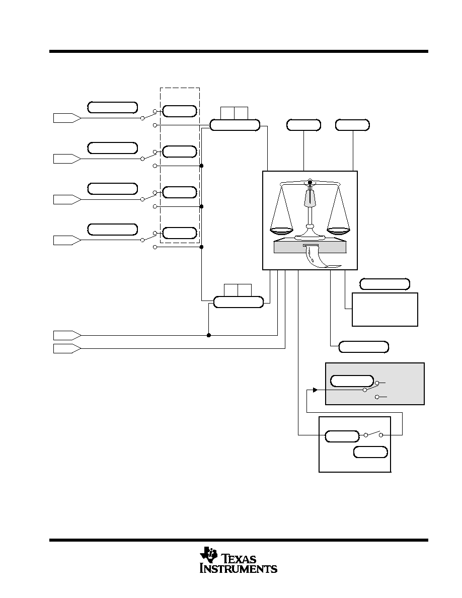
TMS370CxCx
8-BIT MICROCONTROLLER
SPNS040B ≠ NOVEMBER 1995 ≠ REVISED FEBRUARY 1997
37
POST OFFICE BOX 1443
∑
HOUSTON, TEXAS 77251≠1443
analog-to-digital converter 2 module (continued)
The ADC2 module block diagram is illustrated in Figure 12.
ADCTL.4 ≠ 3
4
3
ADENA.0
REF VOLTS SELECT
ADCTL.1 ≠ 0
1
0
AD INPUT SELECT
ADIN.0
Port E Input
ENA 0
Port E Data
AN 0
AN0
ADENA.1
ADIN.1
Port E Input
ENA 1
Port E Data
AN 1
AN1
ADENA.2
ADIN.2
Port E Input
ENA 2
Port E Data
AN 2
AN2
ADENA.3
ADIN.3
Port E Input
ENA 3
Port E Data
AN 3
AN3
VCC
VSS
ADCTL.6
SAMPLE
START
ADCTL.7
CONVERT
START
ADDATA.7 ≠ 0
A-to-D
Conversion
Data Register
ADSTAT.2
AD READY
AD PRIORITY
ADPRI.6
0
1
Level 1 INT
Level 2 INT
AD INT FLAG
ADSTAT.1
AD INT ENA
ADSTAT.0
A/D
Figure 12. ADC2 Block Diagram

TMS370CxCx
8-BIT MICROCONTROLLER
SPNS040B ≠ NOVEMBER 1995 ≠ REVISED FEBRUARY 1997
38
POST OFFICE BOX 1443
∑
HOUSTON, TEXAS 77251≠1443
analog-to-digital converter 2 module (continued)
Table 28. A / D CONTROL REGISTER (ADCTL)
Bit #
7
6
5
4
3
2
1
0
P070
CONVERT
START
SAMPLE
START
--
REF VOLT
SELECT1
REF VOLT
SELECT0
--
AD INPUT
SELECT1
AD INPUT
SELECT0
R W≠ 0
RW ≠ 0
RW ≠ 0
RW ≠ 0
RW ≠ 0
RW ≠ 0
RW ≠ 0
R = read, W = write, ≠
n = value of the bit after the register is reset
Bits 0≠1
AD INPUT SELECT 0≠1 (analog input channel select bits 0 ≠ 1)
These bits select the channel used for conversion. Channels should be changed only after the
ADC2 module has cleared the SAMPLE START and CONVERT START bits. Changing the
channel while either SAMPLE START or CONVERT START is 1 invalidates the conversion in
progress.
Table 29. Analog-Input Channel Selection
AD INPUT
SELECT 1
AD INPUT
SELECT 0
AD INPUT
CHANNEL
0
0
1
1
0
1
0
1
AN0
AN1
AN2
AN3
Bit 2
Reserved (read data is indeterminate)
Bits 3≠4
REF VOLT SELECT 3≠4 (reference voltage (+V
REF
) select bits 3≠4)
These bits select the channel the ADC2 module uses for the positive voltage reference. These
bits must not change during the entire conversion.
Table 30. Voltage-Channel Selection
REF VOLT
SELECT 1
REF VOLT
SELECT 0
+VREF
SOURCE
0
0
1
1
0
1
0
1
VCC
AN1
AN2
AN3
Bit 5
Reserved (read data is indeterminate)
Bit 6
SAMPLE START (sample start)
Setting this bit stops any ongoing conversion and starts sampling the selected input channel to
begin a new conversion. This bit is cleared by the ADC2 module. Entering HALT or STANDBY
mode clears this bit and aborts any sampling in progress.
Bit 7
CONVERT START (conversion start)
Setting this bit starts the conversion. This bit is cleared by the ADC2 module. Entering HALT or
STANDBY mode clears this bit and aborts any conversion in progress.

TMS370CxCx
8-BIT MICROCONTROLLER
SPNS040B ≠ NOVEMBER 1995 ≠ REVISED FEBRUARY 1997
39
POST OFFICE BOX 1443
∑
HOUSTON, TEXAS 77251≠1443
analog-to-digital converter 2 module (continued)
Table 31. A / D Control Register (ADSTAT)
Bit #
7
6
5
4
3
2
1
0
P071
--
--
--
--
--
AD
READY
AD INT
FLAG
AD INT
ENA
R ≠ 0
RC ≠ 0
RW ≠ 0
R = read, W = write, C = clear only, ≠
n = value of the bit after the register is reset
Bit 0
AD INT ENA (A / D interrupt enable)
This bit controls the ADC2 module's ability to generate an interrupt.
0 = Disable A/D interrupt
1 = Enable A/D interrupt
Bit 1
AD INT FLAG (A/D interrupt flag)
The ADC2 module sets this bit at the end of an ADC2 conversion. If this bit is set while the A/D
INT ENA bit is set, an interrupt request is generated. Clearing this flag clears pending A/D interrupt
requests. This bit is cleared by the system reset or by entering HALT or STANDBY mode. Software
cannot set this bit.
Bit 2
AD READY (A/D converter ready)
The ADC2 module sets this bit whenever a conversion is not in progress and the ADC2 is ready
for a new conversion to start. Writing to this bit has no effect on its state.
0 = Conversion is in process
1 = Converter is ready
Bits 3≠7
Reserved (read data is indeterminate)
Table 32. A / D
Conversion Data Register (DATA)
Bit #
7
6
5
4
3
2
1
0
P072
DATA 7
DATA 6
DATA 5
DATA 4
DATA 3
DATA 2
DATA 1
DATA 0
R ≠ 0
R ≠ 0
R ≠ 0
R ≠ 0
R ≠ 0
R ≠ 0
R ≠ 0
R ≠ 0
R = read, ≠
n = value of the bit after the register is reset
The analog-to-digital conversion data is loaded into this register at the end of a conversion and remains until
replaced by another conversion.
Table 33. AN0≠AN3 Port E0 ≠ E3 Data Input Register (ADIN)
¡¡¡
¡¡¡
¡¡¡¡¡
¡¡¡¡¡
¡¡¡¡¡
¡¡¡¡¡
¡¡¡¡
¡¡¡¡
¡¡¡¡¡
¡¡¡¡¡
¡¡¡¡¡
¡¡¡¡¡
¡¡¡¡¡
¡¡¡¡¡
¡¡¡¡
¡¡¡¡
¡¡¡¡¡
¡¡¡¡¡
¡
¡
¡¡¡
Bit #
¡¡¡¡¡
7
¡¡¡¡¡
6
¡¡¡¡
5
¡¡¡¡¡
4
¡¡¡¡¡
3
¡¡¡¡¡
2
¡¡¡¡
1
¡¡¡¡¡
0
¡
¡¡¡
¡
¡
¡
¡¡¡
P07D
¡¡¡¡¡
¡
¡¡¡
¡
¡¡¡¡¡
--
¡¡¡¡¡
¡
¡¡¡
¡
¡¡¡¡¡
--
¡¡¡¡
¡
¡¡
¡
¡¡¡¡
--
¡¡¡¡¡
¡
¡¡¡
¡
¡¡¡¡¡
--
¡¡¡¡¡
¡
¡¡¡
¡
¡¡¡¡¡
DATA IN
AN3
¡¡¡¡¡
¡
¡¡¡
¡
¡¡¡¡¡
DATA IN
AN2
¡¡¡¡
¡
¡¡
¡
¡¡¡¡
DATA IN
AN1
¡¡¡¡¡
¡
¡¡¡
¡
¡¡¡¡¡
DATA IN
AN0
¡
¡
¡
¡¡¡
¡¡¡
¡¡¡¡¡
¡¡¡¡¡
¡¡¡¡¡
¡¡¡¡¡
¡¡¡¡
¡¡¡¡
¡¡¡¡¡
¡¡¡¡¡
¡¡¡¡¡
¡¡¡¡¡
R ≠ 0
¡¡¡¡¡
¡¡¡¡¡
R ≠ 0
¡¡¡¡
¡¡¡¡
R ≠ 0
¡¡¡¡¡
¡¡¡¡¡
R ≠ 0
¡
¡
¡¡¡
¡¡¡¡¡
¡¡¡¡¡
¡¡¡¡
¡¡¡¡¡
¡¡¡¡¡
¡¡¡¡¡
¡¡¡¡
¡¡¡¡¡
¡
R = read, ≠
n = value of the bit after the register is reset

TMS370CxCx
8-BIT MICROCONTROLLER
SPNS040B ≠ NOVEMBER 1995 ≠ REVISED FEBRUARY 1997
40
POST OFFICE BOX 1443
∑
HOUSTON, TEXAS 77251≠1443
analog-to-digital converter 2 module (continued)
Bits 0≠3
PORT E DATA AN0≠AN3 (Analog port E data in)
The ADIN register shows the data present at the pins configured for general-purpose input instead
of ADC2 channels. A bit is configured as general-purpose input if the corresponding bit of the port
enable register is a 1. Pins configured as ADC2 channels are read as 0s. Writing to this address
has no effect.
Bits 4≠7
Reserved (read data is indeterminate)
Table 34. AN0 ≠ AN3 Port E0 ≠E3 Data Input-Enable Register (ADENA)
Bit #
7
6
5
4
3
2
1
0
P07E
--
--
--
--
INPUT
ENA 3
INPUT
ENA 2
INPUT
ENA 1
INPUT
ENA 0
RW ≠ 0
RW ≠ 0
RW ≠ 0
R W≠ 0
R = read, W = write, ≠
n = value of the bit after the register is reset
Bits 0≠3
INPUT ENA 0≠3 (Analog port E input enable)
The ADENA register individually configures the pins AN0≠AN3 as either analog-input channels
or as general-purpose input pins.
0 = The pin becomes an analog-input channel for the ADC2. When the bit is 0, the
corresponding bit in the ADIN register reads 0.
1 = Enables the pin as a general-purpose input pin and its digital value can be read from the
corresponding bit in the ADIN register.
Bits 4≠7
Reserved (read data is indeterminate)
Table 35. Analog Interrupt Priority / Conversion Rate Register (ADPRI)
Bit #
7
6
5
4
3
2
1
0
P07F
AD
STEST
AD
PRIORITY
AD
ESPEN
--
--
--
--
--
RP ≠ 0
RP ≠ 0
RP ≠ 0
RW ≠ 0
R W≠ 0
R = read, W = write, P = privileged write, ≠
n = value of the bit after the register is reset
Bits 0≠4
Reserved (read data is indeterminate)
Bit 5
AD ESPEN (emulator suspend enable)
Normally this bit has no effect. However, when using the XDS emulator to debug a program, this
bit determines what happens to the ADC2 when the program is suspended by an action such as
a hardware or software breakpoint.
0 = When the emulator is suspended, the ADC2 continues to run until the conversion is
complete
1 = When the emulator is suspended, the ADC2 is frozen so that its state can be examined at
the point that the emulator was suspended. The conversion data is indeterminate upon
restart.

TMS370CxCx
8-BIT MICROCONTROLLER
SPNS040B ≠ NOVEMBER 1995 ≠ REVISED FEBRUARY 1997
41
POST OFFICE BOX 1443
∑
HOUSTON, TEXAS 77251≠1443
analog-to-digital converter 2 module (continued)
Bit 6
AD PRIORITY (A/D interrupt priority select)
This bit selects the priority level of the A/D interrupt.
0 = A/D Interrupt is a higher priority (level 1) request.
1 = A/D Interrupt is a lower priority (level 2) request.
Bit 7
AD STEST (this bit must be cleared to ensure proper operation)
instruction set overview
Table 36 provides an opcode-to-instruction cross-reference of all 73 instructions and 274 opcodes of the
`370CxCx instruction set. The numbers at the top of this table represent the most significant nibble of the opcode
while the numbers at the left side of the table represent the least significant nibble. The instructions for these
two opcode nibbles contain the mnemonic, operands, and byte / cycle specific to that opcode.
For example, the opcode B5h points to the CLR A instruction. This instruction contains one byte and executes
in eight SYSCLK cycles.

TMS370CxCx
8-BIT MICROCONTROLLER
SPNS040B ≠ NOVEMBER 1995 ≠ REVISED FEBRUAR
Y
1997
T
emp
l
ate
R
e
l
ease
D
ate:
7
≠
11
≠
94
42
POST
OFFICE BOX 1443 HOUST
ON,
TEXAS
77251≠1443
∑
Table 36. TMS370 Family Opcode/Instruction Map
MSN
0
1
2
3
4
5
6
7
8
9
A
B
C
D
E
F
0
JMP
#ra
2/7
INCW
#ra,Rd
3/11
MOV
Ps,A
2/8
CLRC /
TST A
1/9
MOV
A,B
1/9
MOV
A,Rd
2/7
TRAP
15
1/14
LDST
n
2/6
1
JN
ra
2/5
MOV
A,Pd
2/8
MOV
B,Pd
2/8
MOV
Rs,Pd
3/10
MOV
Ps,B
2/7
MOV
B,Rd
2/7
TRAP
14
1/14
MOV
#ra[SP],A
2/7
2
JZ
ra
2/5
MOV
Rs,A
2/7
MOV
#n,A
2/6
MOV
Rs,B
2/7
MOV
Rs,Rd
3/9
MOV
#n,B
2/6
MOV
B,A
1/8
MOV
#n,Rd
3/8
MOV
Ps,Rd
3/10
DEC
A
1/8
DEC
B
1/8
DEC
Rd
2/6
TRAP
13
1/14
MOV
A,*ra[SP]
2/7
3
JC
ra
2/5
AND
Rs,A
2/7
AND
#n,A
2/6
AND
Rs,B
2/7
AND
Rs,Rd
3/9
AND
#n,B
2/6
AND
B,A
1/8
AND
#n,Rd
3/8
AND
A,Pd
2/9
AND
B,Pd
2/9
AND
#n,Pd
3/10
INC
A
1/8
INC
B
1/8
INC
Rd
2/6
TRAP
12
1/14
CMP
*n[SP],A
2/8
4
JP
ra
2/5
OR
Rs,A
2/7
OR
#n,A
2/6
OR
Rs,B
2/7
OR
Rs,Rd
3/9
OR
#n,B
2/6
OR
B,A
1/8
OR
#n,Rd
3/8
OR
A,Pd
2/9
OR
B,Pd
2/9
OR
#n,Pd
3/10
INV
A
1/8
INV
B
1/8
INV
Rd
2/6
TRAP
11
1/14
extend
inst,2
opcodes
L
S
5
JPZ
ra
2/5
XOR
Rs,A
2/7
XOR
#n,A
2/6
XOR
Rs,B
2/7
XOR
Rs,Rd
3/9
XOR
#n,B
2/6
XOR
B,A
1/8
XOR
#n,Rd
3/8
XOR
A,Pd
2/9
XOR
B,Pd
2/9
XOR
#n,Pd
3/10
CLR
A
1/8
CLR
B
1/8
CLR
Rn
2/6
TRAP
10
1/14
S
N
6
JNZ
ra
2/5
BTJO
Rs,A,ra
3/9
BTJO
#n,A,ra
3/8
BTJO
Rs,B,ra
3/9
BTJO
Rs,Rd,ra
4/11
BTJO
#n,B,ra
3/8
BTJO
B,A,ra
2/10
BTJO
#n,Rd,ra
4/10
BTJO
A,Pd,ra
3/11
BTJO
B,Pd,ra
3/10
BTJO
#n,Pd,ra
4/11
XCHB
A
1/10
XCHB A /
TST B
1/10
XCHB
Rn
2/8
TRAP
9
1/14
IDLE
1/6
7
JNC
ra
2/5
BTJZ
Rs.,A,ra
3/9
BTJZ
#n,A,ra
3/8
BTJZ
Rs,B,ra
3/9
BTJZ
Rs,Rd,ra
4/11
BTJZ
#n,B,ra
3/8
BTJZ
B,A,ra
2/10
BTJZ
#n,Rd,ra
4/10
BTJZ
A,Pd,ra
3/10
BTJZ
B,Pd,ra
3/10
BTJZ
#n,Pd,ra
4/11
SWAP
A
1/11
SWAP
B
1/11
SWAP
Rn
2/9
TRAP
8
1/14
MOV
#n,Pd
3/10
8
JV
ra
2/5
ADD
Rs,A
2/7
ADD
#n,A
2/6
ADD
Rs,B
2/7
ADD
Rs,Rd
3/9
ADD
#n,B
2/6
ADD
B,A
1/8
ADD
#n,Rd
3/8
MOVW
#16,Rd
4/13
MOVW
Rs,Rd
3/12
MOVW
#16[B],Rpd
4/15
PUSH
A
1/9
PUSH
B
1/9
PUSH
Rd
2/7
TRAP
7
1/14
SETC
1/7
9
JL
ra
2/5
ADC
Rs,A
2/7
ADC
#n,A
2/6
ADC
Rs,B
2/7
ADC
Rs,Rd
3/9
ADC
#n,B
2/6
ADC
B,A
1/8
ADC
#n,Rd
3/8
JMPL
lab
3/9
JMPL
*Rp
2/8
JMPL
*lab[B]
3/11
POP
A
1/9
POP
B
1/9
POP
Rd
2/7
TRAP
6
1/14
RTS
1/9
A
JLE
ra
2/5
SUB
Rs,A
2/7
SUB
#n,A
2/6
SUB
Rs,B
2/7
SUB
Rs,Rd
3/9
SUB
#n,B
2/6
SUB
B,A
1/8
SUB
#n,Rd
3/8
MOV
& lab,A
3/10
MOV
*Rp,A
2/9
MOV
*lab[B],A
3/12
DJNZ
A,#ra
2/10
DJNZ
B,#ra
2/10
DJNZ
Rd,#ra
3/8
TRAP
5
1/14
RTI
1/12
B
JHS
ra
2/5
SBB
Rs,A
2/7
SBB
#n,A
2/6
SBB
Rs,B
2/7
SBB
Rs,Rd
3/9
SBB
#n,B
2/6
SBB
B,A
1/8
SBB
#n,Rd
3/8
MOV
A, & lab
3/10
MOV
A, *Rp
2/9
MOV
A,*lab[B]
3/12
COMPL
A
1/8
COMPL
B
1/8
COMPL
Rd
2/6
TRAP
4
1/14
PUSH
ST
1/8
All conditional jumps (opcodes 01-0F), BTJO, BTJZ, and DJNZ instructions use two additional cycles if the branch is taken. The BTJO, BTJZ, and DJNZ instructions
have a relative address as the last operand.
L

TMS370CxCx
8-BIT MICROCONTROLLER
SPNS040B ≠ NOVEMBER 1995 ≠ REVISED FEBRUAR
Y
1997
POST
OFFICE BOX 1443 HOUST
ON,
TEXAS
77251≠1443
∑
43
Table 36. TMS370 Family Opcode/Instruction Map
(Continued)
MSN
0
1
2
3
4
5
6
7
8
9
A
B
C
D
E
F
C
JNV
ra
2/5
MPY
Rs,A
2/46
MPY
#n,A
2/45
MPY
Rs,B
2/46
MPY
Rs,Rd
3/48
MPY
#n,B
2/45
MPY
B,A
1/47
MPY
#n,Rs
3/47
BR
lab
3/9
BR
*Rp
2/8
BR
*lab[B]
3/11
RR
A
1/8
RR
B
1/8
RR
Rd
2/6
TRAP
3
1/14
POP
ST
1/8
L
S
D
JGE
ra
2/5
CMP
Rs,A
2/7
CMP
#n,A
2/6
CMP
Rs,B
2/7
CMP
Rs,Rd
3/9
CMP
#n,B
2/6
CMP
B,A
1/8
CMP
#n,Rd
3/8
CMP
& lab,A
3/11
CMP
*Rp,A
2/10
CMP
*lab[B],A
3/13
RRC
A
1/8
RRC
B
1/8
RRC
Rd
2/6
TRAP
2
1/14
LDSP
1/7
S
N
E
JG
ra
2/5
DAC
Rs,A
2/9
DAC
#n,A
2/8
DAC
Rs,B
2/9
DAC
Rs,Rd
3/11
DAC
#n,B
2/8
DAC
B,A
1/10
DAC
#n,Rd
3/10
CALL
lab
3/13
CALL
*Rp
2/12
CALL
*lab[B]
3/15
RL
A
1/8
RL
B
1/8
RL
Rd
2/6
TRAP
1
1/14
STSP
1/8
F
JLO
ra
2/5
DSB
Rs,A
2/9
DSB
#n,A
2/8
DSB
Rs,B
2/9
DSB
Rs,Rd
3/11
DSB
#n,B
2/8
DSB
B,A
1/10
DSB
#n,Rd
3/10
CALLR
lab
3/15
CALLR
*Rp
2/14
CALLR
*lab[B]
3/17
RLC
A
1/8
RLC
B
1/8
RLC
Rd
2/6
TRAP
0
1/14
NOP
1/7
Second byte of two-byte instructions (F4xx):
F4
8
MOVW
*n[Rn]
4/15
DIV
Rn.A
3/14-63
F4
9
JMPL
*n[Rn]
4/16
Legend:
*
= Indirect addressing operand prefix
&
= Direct addressing operand prefix
F4
A
MOV
*n[Rn],A
4/17
#
= immediate operand
#16 = immediate 16-bit number
lab = 16-label
i
di t 8 bit
b
F4
B
MOV
A,*n[Rn]
4/16
n
= immediate 8-bit number
Pd = Peripheral register containing destination type
Pn = Peripheral register
Ps = Peripheral register containing source byte
F4
C
BR
*n[Rn]
4/16
Ps = Peri heral register containing source byte
ra
= Relative address
Rd = Register containing destination type
Rn = Register file
F4
D
CMP
*n[Rn],A
4/18
Rn
Register file
Rp = Register pair
Rpd = Destination register pair
Rps = Source Register pair
F4
E
CALL
*n[Rn]
4/20
Rs = Register containing source byte
F4
F
CALLR
*n[Rn]
4/22
All conditional jumps (opcodes 01-0F), BTJO, BTJZ, and DJNZ instructions use two additional cycles if the branch is taken. The BTJO, BTJZ, and DJNZ instructions
have a relative address as the last operand.

TMS370CxCx
8-BIT MICROCONTROLLER
SPNS040B ≠ NOVEMBER 1995 ≠ REVISED FEBRUARY 1997
44
POST OFFICE BOX 1443
∑
HOUSTON, TEXAS 77251≠1443
development system support
The TMS370 family development support tools include an assembler, a C compiler, a linker, a compact
development tool, and an EEPROM / UVEPROM programmer.
D
Assembler / linker (Part No. TMDS3740850≠02 for PC)
≠
Includes extensive macro capability
≠
Allows high-speed operation
≠
Provides format conversion utilities for popular formats.
D
ANSI C Compiler (Part No. TMDS3740855≠02 for PC, Part No. TMDS3740555≠09 for HP700
TM
, Sun-3
TM
or Sun-4
TM
)
≠
Generates assembly code for the TMS370 that can be inspected easily
≠
Improves code execution speed and reduces code size with optional optimizer pass
≠
Enables direct reference to the TMS370's port registers by using a naming convention
≠
Provides flexibility in specifying the storage for data objects
≠
Interfaces C functions and assembly functions easily
≠
Includes assembler and linker
D
CDT370 (compact development tool) real-time in-circuit emulation
≠
Base (Part Number EDSCDT370 ≠ for PC, requires cable)
≠
Cable for 28-pin PLCC (Part No. EDSTRG28PLCCCX)
≠
Cable for 28-pin DIP (Part No. EDSTRG28DILCX)
≠
Includes EEPROM and EPROM programming support
≠
Allows inspection and modification of memory locations
≠
Allows uploading / downloading program and data memory
≠
Executes programs and software routines
≠
Includes 1 024 samples trace buffer
≠
Provides single-step executable instructions
≠
Uses software breakpoints to halt program execution at selected address
D
Microcontroller programmer
≠
Base (Part No. TMDS3760500A ≠ for PC, requires programmer head)
≠
Single unit head for 28-pin PLCC/DIP (Part No. TMDS3780514A)
≠
Personal computer based, window / function-key-oriented user interface for ease of use and rapid
learning environment
HP700 is a trademark of Hewlett-Packard Company.
Sun-3 and Sun-4 are trademarks of Sun Microsystems, Incorporated.
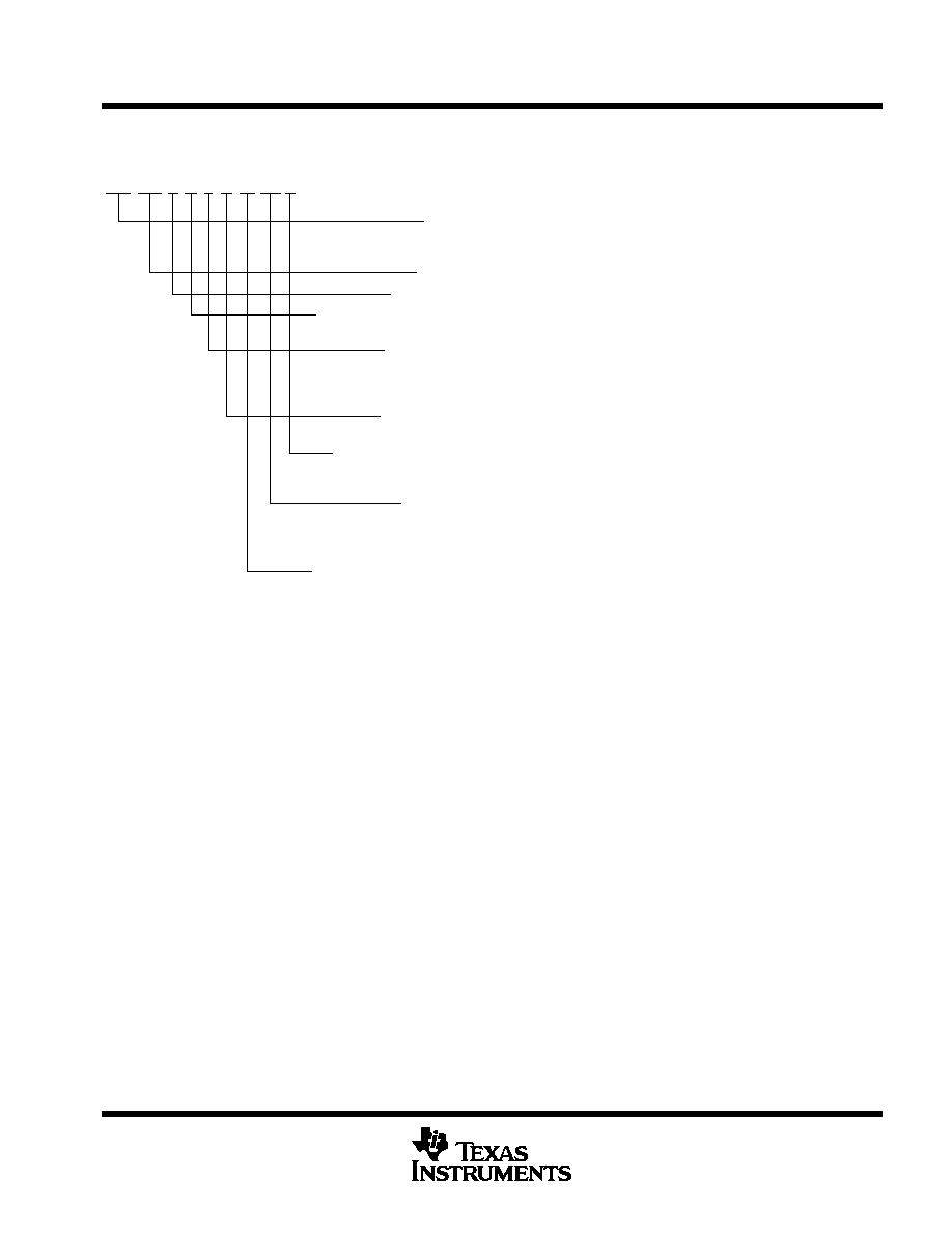
TMS370CxCx
8-BIT MICROCONTROLLER
SPNS040B ≠ NOVEMBER 1995 ≠ REVISED FEBRUARY 1997
45
POST OFFICE BOX 1443
∑
HOUSTON, TEXAS 77251≠1443
device numbering conventions
Figure 13 illustrates the numbering and symbol nomenclature for the TMS370CxCx family.
3
370
C 0
C
Prefix: TMS = Standard prefix for fully qualified devices
SE = System evaluator that is used for
prototyping purpose.
Family:
370 = TMS370 8-Bit Microcontroller Family
Technology:
C = CMOS
Program Memory Types:
3 = Mask ROM, No Data EEPROM
6 = EPROM, No Data EEPROM
Device Type:
C = 'xCx devices containing the following modules:
-- Timer 1
-- Analog-to-Digital Converter 2 (ADC2)
-- Serial Communications Interface 2 (SCI2)
Memory Size:
0 = 4K bytes
2 = 8K bytes
Temperature Ranges:
A = ≠40
∞
C to
85
∞
C
L =
0
∞
C to
70
∞
C
T = ≠40
∞
C to
105
∞
C
Packages:
FN = Plastic Leaded Chip Carrier
FZ = Ceramic Leaded Chip Carrier
N = Plastic Dual-In-Line
JD = Ceramic Dual-In-Line
ROM and EPROM Option:
A = For ROM device, the watchdog timer can be configured
as one of the three different mask options:
≠ A standard watchdog
≠ A hard watchdog
≠ A simple watchdog
The clock mask option can be:
≠ Divide-by-4 clock
≠ Divide-by-1 (PLL) clock
The low-power modes can be:
≠ Enabled
≠ Disabled
TMS
A FN L
Figure 13. TMS370CxCx Family Nomenclature
TMS370CxCx
8-BIT MICROCONTROLLER
SPNS040B ≠ NOVEMBER 1995 ≠ REVISED FEBRUARY 1997
46
POST OFFICE BOX 1443
∑
HOUSTON, TEXAS 77251≠1443
device part numbers
Table 37 lists all of the 'xCx devices available. The devices' part number nomenclature is designed to assist
ordering. Upon ordering, the customer must specify not only the device part number, but also the clock and
watchdog timer options desired. Each device can have only one of the three possible watchdog timer options
and one of the two clock options. The required options information pertains solely to orders involving ROM
devices.
Table 37. Device Part Numbers
DEVICE PART NUMBERS
FOR 28 PINS (LCC)
FOR 28 PINS (DIP)
TMS370C3C0AFNA
TMS370C3C0AFNL
TMS370C3C0AFNT
TMS370C3C0ANA
TMS370C3C0ANL
TMS370C3C0ANT
TMS370C6C2AFNT
TMS370C6C2ANT
SE370C6C2AFZT
SE370C6C2AJDT
System evaluators are for use in prototype environment and their
reliability has not been characterized.

TMS370CxCx
8-BIT MICROCONTROLLER
SPNS040B ≠ NOVEMBER 1995 ≠ REVISED FEBRUARY 1997
47
POST OFFICE BOX 1443
∑
HOUSTON, TEXAS 77251≠1443
new code release form
Figure 14 shows a sample of the new code release form.
NEW CODE RELEASE FORM
TEXAS INSTRUMENTS
TMS370 MICROCONTROLLER PRODUCTS
DATE:
To release a new customer algorithm to TI incorporated into a TMS370 family microcontroller, complete this form and submit with the following information:
1. A ROM description in object form on Floppy Disk, Modem XFR, or EPROM (Verification file will be returned via same media)
2. An attached specification if not using TI standard specification as incorporated in TI's applicable device data book.
Company Name:
Street Address:
Street Address:
City:
State
Zip
Contact Mr./Ms.:
Phone: (
)
Ext.:
Customer Purchase Order Number:
Customer Part Number:
Customer Application:
Customer Print Number *Yes:
#
No:
(Std. spec to be followed)
*If Yes: Customer must provide "print" to TI w/NCRF for approval before ROM
code processing starts.
TMS370 Device:
TI Customer ROM Number:
(provided by Texas Instruments)
CONTACT OPTIONS FOR THE 'A' VERSION TMS370 MICROCONTROLLERS
OSCILLATOR FREQUENCY
MIN
TYP
MAX
[] External Drive (CLKIN)
[] Crystal
[] Ceramic Resonator
Low Power Modes
[] Enabled
[] Disabled
Watchdog counter
[] Standard
[] Hard Enabled
[] Simple Counter
Clock Type
[] Standard (/4)
[] PLL (/1)
[] Supply Voltage MIN:
MAX:
(std range: 4.5V to 5.5V)
NOTE:
Non 'A' version ROM devices of the TMS370 microcontrollers will have the
"Low-power modes Enabled", "Divide-by-4" Clock, and "Standard" Watchdog
options. See the
TMS370 Family User's Guide (literature number SPNU127)
or the
TMS370 Family Data Manual (literature number SPNS014B).
TEMPERATURE RANGE
[] 'L':
0
∞
to 70
∞
C (standard)
[] 'A':
≠40
∞
to 85
∞
C
[] 'T':
≠40
∞
to 105
∞
C
PACKAGE TYPE
[] 'N' 28-pin PDIP
[] "FN" 44-pin PLCC
[] "FN" 28-pin PLCC
[] "FN" 68-pin PLCC
[] "N" 40-pin PDIP
[] "NM" 64-pin PSDIP
[] "NJ" 40-pin PSDIP (formerly known as N2)
SYMBOLIZATION
BUS EXPANSION
[] TI standard symbolization
[] TI standard w/customer part number
[] Customer symbolization
(per attached spec, subject to approval)
[] YES
[] NO
NON-STANDARD SPECIFICATIONS:
ALL NON-STANDARDS SPECIFICATIONS MUST BE APPROVED BY THE TI ENGINEERING STAFF: If the customer requires expedited production material
(i.e., product which must be started in process prior to prototype approval and full production release) and non-standard spec issues are not resolved to the
satisfaction of both the customer and TI in time for a scheduled shipment, the specification parameters in question will be processed/tested to the standard
TI spec. Any such devices which are shipped without conformance to a mutually approved spec, will be identified by a 'P' in the symbolization preceding the
TI part number.
RELEASE AUTHORIZATION:
This document, including any referenced attachments, is and will be the controlling document for all orders placed for this TI custom device. Any changes must
be in writing and mutually agreed to by both the customer and TI. The prototype cycletime commences when this document is signed off and the verification
code is approved by the customer.
1. Customer:
Date:
2. TI: Field Sales:
Marketing:
Prod. Eng.:
Proto. Release:
Figure 14. Sample New Code Release Form
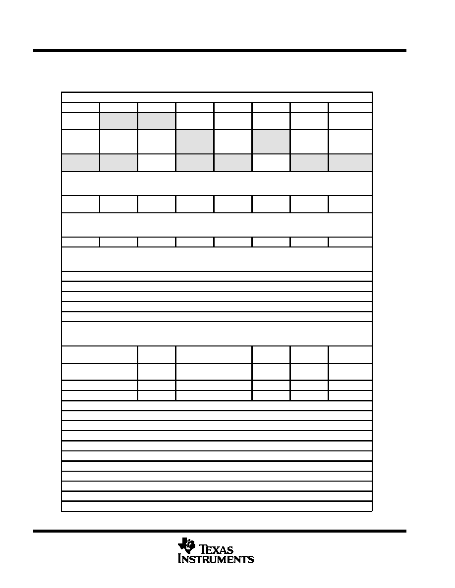
TMS370CxCx
8-BIT MICROCONTROLLER
SPNS040B ≠ NOVEMBER 1995 ≠ REVISED FEBRUARY 1997
48
POST OFFICE BOX 1443
∑
HOUSTON, TEXAS 77251≠1443
Table 38 is a collection of all the peripheral file frames used in the 'CxCx (provided for a quick reference).
Table 38. Peripheral File Frame Compilation
System Configuration Registers
PF
BIT 7
BIT 6
BIT 5
BIT 4
BIT 3
BIT 2
BIT 1
BIT 0
REG
P010
COLD
START
OSC
POWER
PF AUTO
WAIT
OSC FLT
FLAG
MC PIN
WPO
MC PIN
DATA
--
µ
P /
µ
C
MODE
SCCR0
P011
--
--
--
AUTO
WAIT
DISABLE
--
MEMORY
DISABLE
--
--
SCCR1
P012
HALT /
STANDBY
PWRDWN /
IDLE
--
BUS
STEST
CPU
STEST
--
INT1
NMI
PRIVILEGE
DISABLE
SCCR2
P013
to
P016
Reserved
P017
INT1
FLAG
INT1
PIN DATA
--
--
--
INT1
POLARITY
INT1
PRIORITY
INT1
ENABLE
INT1
P018
to
P01B
Reserved
P01C
BUSY
VPPS
--
--
--
--
W0
EXE
EPCTL
P01D
P01E
P01F
Reserved
Digital Port-Control Registers
P020
Reserved
APORT1
P021
Port A Control Register 2 (must be 0)
APORT2
P022
Port A Data
ADATA
P023
Port A Direction
ADIR
P024
to
P02B
Reserved
P02C
Port D Control Register 1
(must be 0)
--
Port D Control Register 1
(must be 0)
--
--
--
DPORT1
P02D
Port D Control Register 2
(must be 0)
--
Port D Control Register 2
(must be 0)
--
--
--
DPORT2
P02E
Port D Data
--
Port D Data
--
--
--
DDATA
P02F
Port D Direction
--
Port D Direction
--
--
--
DDIR
Timer 1 Module Register Memory Map
Modes: Dual-Compare and Capture/Compare
P040
Bit 15
T1Counter MSbyte
Bit 8
T1CNTR
P041
Bit 7
T1 Counter LSbyte
Bit 0
P042
Bit 15
Compare Register MSbyte
Bit 8
T1C
P043
Bit 7
Compare Register LSbyte
Bit 0
P044
Bit 15
Capture/Compare Register MSbyte
Bit 8
T1CC
P045
Bit 7
Capture/Compare Register LSbyte
Bit 0
P046
Bit 15
Watchdog Counter MSbyte
Bit 8
WDCNTR
P047
Bit 7
Watchdog Counter LSbyte
Bit 0
P048
Bit 7
Watchdog Reset Key
Bit 0
WDRST
To configure pin D3 as SYSCLK, set port D control register 2 = 08h.

TMS370CxCx
8-BIT MICROCONTROLLER
SPNS040B ≠ NOVEMBER 1995 ≠ REVISED FEBRUARY 1997
49
POST OFFICE BOX 1443
∑
HOUSTON, TEXAS 77251≠1443
Table 38. Peripheral File Frame Compilation (Continued)
PF
BIT 7
BIT 6
BIT 5
BIT 4
BIT 3
BIT 2
BIT 1
BIT 0
REG
Mode: Dual-Compare and Capture/Compare (Continued)
P049
WD OVRFL
TAP SEL
WD INPUT
SELECT2
WD INPUT
SELECT1
WD INPUT
SELECT0
--
T1 INPUT
SELECT2
T1 INPUT
SELECT1
T1 INPUT
SELECT0
T1CTL1
P04A
WD OVRFL
RST ENA
WD OVRFL
INT ENA
WD OVRFL
INT FLAG
T1 OVRFL
INT ENA
T1 OVRFL
INT FLAG
--
--
T1
SW RESET
T1CTL2
Mode: Dual-Compare
P04B
T1EDGE
INT FLAG
T1C2
INT FLAG
T1C1
INT FLAG
--
--
T1EDGE
INT ENA
T1C2
INT ENA
T1C1
INT ENA
T1CTL3
P04C
T1 MODE=0
T1C1
OUT ENA
T1C2
OUT ENA
T1C1
RST ENA
T1CR
OUT ENA
T1EDGE
POLARITY
T1CR
RST ENA
T1EDGE
DET ENA
T1CTL4
Mode: Capture / Compare
P04B
T1EDGE
INT FLAG
--
T1C1
INT FLAG
--
--
T1EDGE
INT ENA
--
T1C1
INT ENA
T1CTL3
P04C
T1
MODE = 1
T1C1
OUT ENA
--
T1C1
RST ENA
--
T1EDGE
POLARITY
--
T1EDGE
DET ENA
T1CTL4
Modes: Dual-Compare and Capture/Compare
P04D
--
--
--
--
T1EVT
DATA IN
T1EVT
DATA OUT
T1EVT
FUNCTION
T1EVT
DATA DIR
T1PC1
P04E
T1PWM
DATA IN
T1PWM
DATA OUT
T1PWM
FUNCTION
T1PWM
DATA DIR
T1IC/CR
DATA IN
T1IC/CR
DATA OUT
T1IC/CR
FUNCTION
T1IC/CR DATA
DIR
T1PC2
P04F
T1 STEST
T1
PRIORITY
--
--
--
--
--
--
T1PRI
SCI2 Module Control Memory Map
P050
STOP BITS
EVEN/ODD
PARITY
PARITY
ENABLE
ASYNC
ENABLE
ADDRESS/
IDLE WUP
SCI CHAR2
SCI CHAR1
SCI CHAR0
SCICCR
P051
--
--
SCI SW
RESET
CLOCK
ENABLE
TXWAKE
SLEEP
TXENA
RXENA
SCICTL
P052
BAUDF
(MSB)
BAUDE
BAUDD
BAUDC
BAUDB
BAUDA
BAUD9
BAUD8
BAUD
MSB
P053
BAUD7
BAUD6
BAUD5
BAUD4
BAUD3
BAUD2
BAUD1
BAUD0 (LSB)
BAUD LSB
P054
TXRDY
TX EMPTY
--
--
--
--
--
SCI TX
INT ENA
TXCTL
P055
RX
ERROR
RXRDY
BRKDT
FE
OE
PE
RXWAKE
SCI RX
INT ENA
RXCTL
P056
Reserved
P057
RXDT7
RXDT6
RXDT5
RXDT4
RXDT3
RXDT2
RXDT1
RXDT0
RXBUF
P058
Reserved
P059
TXDT7
TXDT6
TXDT5
TXDT4
TXDT3
TXDT2
TXDT1
TXDT0
TXBUF
P05A
to
P05D
Reserved
P05E
SCITXD
DATA IN
SCITXD
DATA OUT
SCITXD
FUNCTION
SCITXD
DATA DIR
SCIRXD
DATA IN
SCIRXD
DATA OUT
SCIRXD
FUNCTION
SCIRXD DATA
DIR
SCIPC2
P05F
SCI STEST
SCITX
PRIORITY
SCIRX
PRIORITY
SCI
ESPEN
--
--
--
--
SCIPRI
Once the WD OVRFL RST ENA bit is set, these bits cannot be changed until a reset; this applies only to the standard
watchdog and to simple counter. In the hard watchdog, these bits can be modified at any time; the WD INPUT SELECT2
bits are ignored.
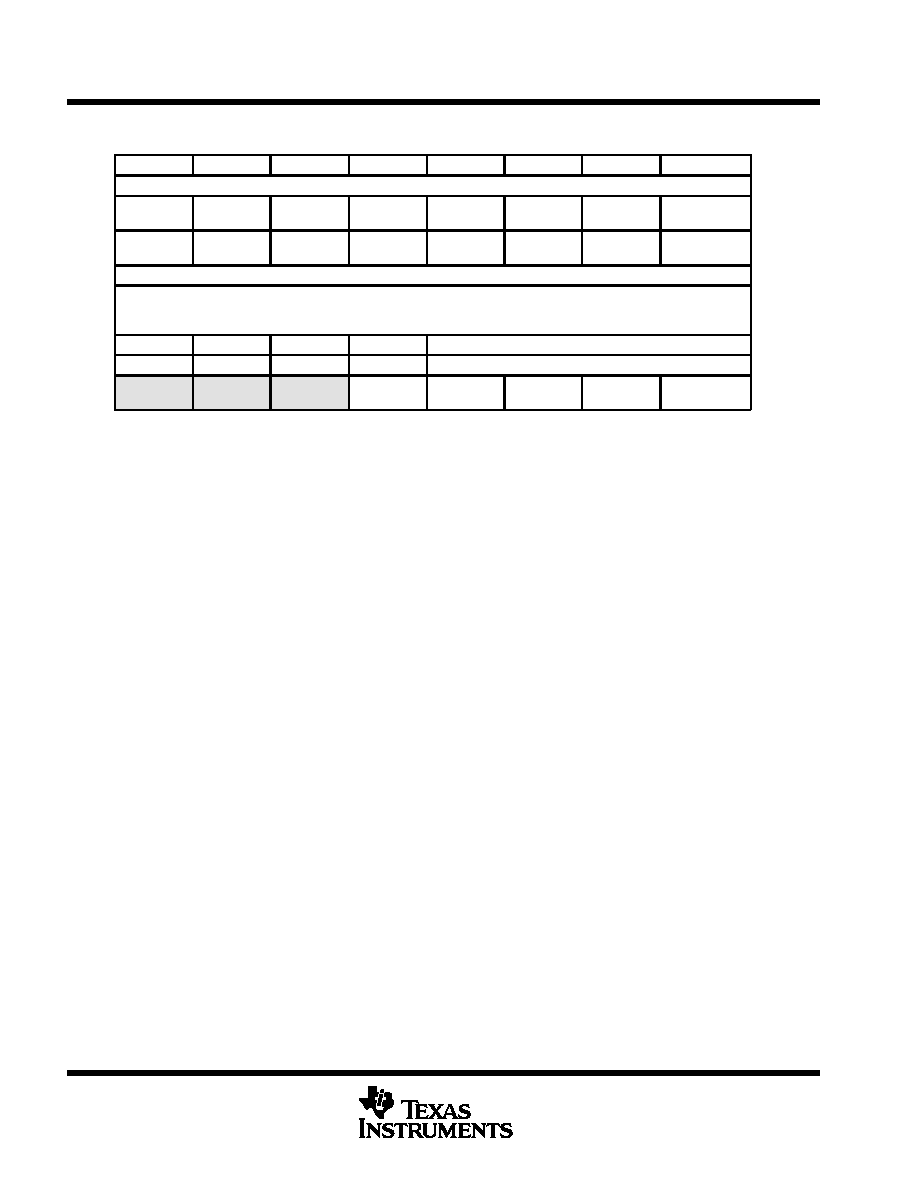
TMS370CxCx
8-BIT MICROCONTROLLER
SPNS040B ≠ NOVEMBER 1995 ≠ REVISED FEBRUARY 1997
50
POST OFFICE BOX 1443
∑
HOUSTON, TEXAS 77251≠1443
Table 38. Peripheral File Frame Compilation (Continued)
PF
BIT 7
BIT 6
BIT 5
BIT 4
BIT 3
BIT 2
BIT 1
BIT 0
REG
ADC2 Module Control Registers
P070
CONVERT
START
SAMPLE
START
--
REF VOLT
SELECT1
REF VOLT
SELECT0
--
AD INPUT
SELECT1
AD INPUT
SELECT0
ADCTL
P071
--
--
--
--
--
AD READY
AD INT
FLAG
AD INT ENA
ADSTAT
P072
A-to-D Conversion Data Register
ADDATA
P073
to
P07C
Reserved
P07D
--
--
--
--
Port E Data Input Register
ADIN
P07E
--
--
--
--
Port E Input Enable Register
ADENA
P07F
AD STEST
AD
PRIORITY
AD ESPEN
--
--
--
--
--
ADPRI
absolute maximum ratings over operating free-air temperature range (unless otherwise noted)
Supply voltage range,V
CC
(see Note 2)
≠ 0.6 V to 7 V
. . . . . . . . . . . . . . . . . . . . . . . . . . . . . . . . . . . . . . . . . . . . . . .
Input voltage range, All pins except MC
≠ 0.6 V to 7 V
. . . . . . . . . . . . . . . . . . . . . . . . . . . . . . . . . . . . . . . . . . . . . .
MC
≠ 0.6 V to 14 V
. . . . . . . . . . . . . . . . . . . . . . . . . . . . . . . . . . . . . . . . . . . . .
Input clamp current, I
IK
(V
I
<
0 or V
I
>
V
CC)
±
20 mA
. . . . . . . . . . . . . . . . . . . . . . . . . . . . . . . . . . . . . . . . . . . . . . . .
Output clamp current, I
OK
(V
O
<
0 or V
O
>
V
CC
)
±
20 mA
. . . . . . . . . . . . . . . . . . . . . . . . . . . . . . . . . . . . . . . . . . . .
Continuous output current per buffer, I
O
(V
O
= 0 to V
CC
) (see Note 3)
±
10 mA
. . . . . . . . . . . . . . . . . . . . . . . . .
Maximum I
CC
current
170 mA
. . . . . . . . . . . . . . . . . . . . . . . . . . . . . . . . . . . . . . . . . . . . . . . . . . . . . . . . . . . . . . . . . . .
Maximum I
SS
current
≠ 170 mA
. . . . . . . . . . . . . . . . . . . . . . . . . . . . . . . . . . . . . . . . . . . . . . . . . . . . . . . . . . . . . . . . . .
Continuous power dissipation
500 mW
. . . . . . . . . . . . . . . . . . . . . . . . . . . . . . . . . . . . . . . . . . . . . . . . . . . . . . . . . . . .
Operating free-air temperature range, T
A:
L version
0
∞
C to 70
∞
C
. . . . . . . . . . . . . . . . . . . . . . . . . . . . . . . . . . . . .
A version
≠ 40
∞
C to 85
∞
C
. . . . . . . . . . . . . . . . . . . . . . . . . . . . . . . . . . .
T version
≠ 40
∞
C to 105
∞
C
. . . . . . . . . . . . . . . . . . . . . . . . . . . . . . . . .
Storage temperature range, T
stg
≠ 65
∞
C to 150
∞
C
. . . . . . . . . . . . . . . . . . . . . . . . . . . . . . . . . . . . . . . . . . . . . . . . . . .
Stresses beyond those listed under "absolute maximum ratings" may cause permanent damage to the device. These are stress ratings only, and
functional operation of the device at these or any other conditions beyond those indicated under "recommended operating conditions" is not
implied. Exposure to absolute-maximum-rated conditions for extended periods may affect device reliability.
NOTES:
2. Unless otherwise noted, all voltage values are with respect to VSS.
3. Electrical characteristics are specified with all output buffers loaded with specified IO current. Exceeding the specified IO current in
any buffer can affect the levels on other buffers.
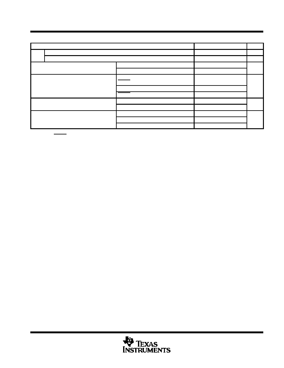
TMS370CxCx
8-BIT MICROCONTROLLER
SPNS040B ≠ NOVEMBER 1995 ≠ REVISED FEBRUARY 1997
51
POST OFFICE BOX 1443
∑
HOUSTON, TEXAS 77251≠1443
recommended operating conditions
MIN
NOM
MAX
UNIT
VCC
Supply voltage (see Note 2)
4.5
5
5.5
V
VCC
RAM data-retention supply voltage (see Note 4)
3
5.5
V
VIL
Low level input voltage
All pins except MC
VSS
0.8
V
VIL
Low-level input voltage
MC, normal operation
VSS
0.3
V
V
Hi h l
l i
t
lt
All pins except MC, XTAL2 / CLKIN, and
RESET
2
VCC
V
VIH
High-level input voltage
XTAL2 / CLKIN
0.8 VCC
VCC
V
RESET
0.7 VCC
VCC
VMC
MC (mode control) voltage
EPROM programming voltage (VPP)
13
13.2
13.5
V
VMC
MC (mode control) voltage
Microcomputer
VSS
0.3
V
L version
0
70
TA
Operating free-air temperature
A version
≠ 40
85
∞
C
T version
≠ 40
105
NOTES:
2. Unless otherwise noted, all voltage values are with respect to VSS.
4. RESET must be activated externally when VCC or SYSCLK is out of the recommended operating range.
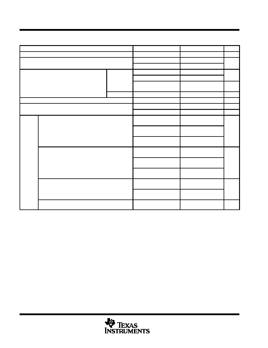
TMS370CxCx
8-BIT MICROCONTROLLER
SPNS040B ≠ NOVEMBER 1995 ≠ REVISED FEBRUARY 1997
52
POST OFFICE BOX 1443
∑
HOUSTON, TEXAS 77251≠1443
electrical characteristics over recommended operating free-air temperature range (unless
otherwise noted)
PARAMETER
TEST CONDITIONS
MIN
TYP
MAX
UNIT
VOL
Low-level output voltage
IOL = 1.4 mA
0.4
V
VOH
High level output voltage
IOH = ≠ 50
µ
A
0.9 VCC
V
VOH
High-level output voltage
IOH = ≠ 2 mA
2.4
V
0 V
VI
0.3 V
10
µ
A
MC
0.3 V < VI
13 V
650
µ
A
II
Input current
MC
12 V
VI
13 V
See Note 5
50
mA
I / O pins
0 V
VI
VCC
±
10
µ
A
IOL
Low-level output current
VOL = 0.4 V
1.4
mA
IOH
High level output current
VOH = 0.9 VCC
≠ 50
µ
A
IOH
High-level output current
VOH = 2.4 V
≠ 2
mA
See Notes 6 and 7
SYSCLK = 5 MHz
20
36
Supply current (operating mode)
OSC POWER bit = 0 (see Note 8)
See Notes 6 and 7
SYSCLK = 3 MHz
13
25
mA
See Notes 6 and 7
SYSCLK = 0.5 MHz
5
11
See Notes 6 and 7
SYSCLK = 5 MHz
10
17
ICC
Supply current (STANDBY mode)
OSC POWER bit = 0 (see Note 9)
See Notes 6 and 7
SYSCLK = 3 MHz
6.5
11
mA
See Notes 6 and 7
SYSCLK = 0.5 MHz
2
3.5
Supply current (STANDBY mode)
See Notes 6 and 7
SYSCLK = 3 MHz
4.5
8.6
mA
y
(
)
OSC POWER bit = 1 (see Note 10)
See Notes 6 and 7
SYSCLK = 0.5 MHz
1.5
3.0
mA
Supply current (HALT mode)
See Note 6
XTAL2 / CLKIN < 0.2 V
1
30
µ
A
NOTES:
5. Input current IPP is a maximum of 50 mA only when you are programming EPROM.
6. Single chip mode, ports configured as inputs or outputs with no load. All inputs
0.2 V or
VCC ≠ 0.2 V.
7. XTAL2/CLKIN is driven with an external square wave signal with 50% duty cycle and rise and fall times less than 10 ns. Current
can be higher with a crystal oscillator. At 5 MHz SYSCLK, this extra current = 0.01 mA x (total load capacitance + crystal capacitance
in pF).
8. Maximum operating current = 5.6 (SYSCLK) + 8 mA.
9. Maximum standby current = 3 (SYSCLK) + 2 mA. (OSC POWER bit = 0).
10. Maximum standby current = 2.24 (SYSCLK) + 1.9 mA. (OSC POWER bit = 1, only valid up to 3 MHz (SYSCLK).
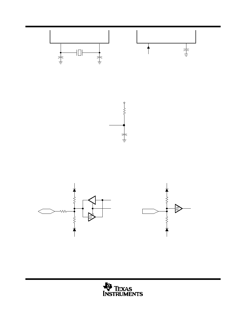
TMS370CxCx
8-BIT MICROCONTROLLER
SPNS040B ≠ NOVEMBER 1995 ≠ REVISED FEBRUARY 1997
53
POST OFFICE BOX 1443
∑
HOUSTON, TEXAS 77251≠1443
External
Clock Signal
XTAL1
XTAL2/CLKIN
C2 (see Note B)
C1
(see Note B)
Crystal/Ceramic
Resonator
(see Note A)
XTAL1
XTAL2/CLKIN
C3 (see Note B)
NOTES: A. The crystal/ceramic resonator frequency is four times the reciprocal of the system clock period.
B. The values of C1 and C2 are typically 15 pF and the value of C3 is typically 50 pF. See the manufacturer's recommendations for
ceramic resonators.
Figure 15. Recommended Crystal/Clock Connections
1.2 k
20 pF
VO
Load Voltage
Case 1: VO = VOH = 2.4 V; Load Voltage = 0 V
Case 2: VO = VOL = 0.4 V; Load Voltage = 2.1 V
NOTE A: All measurements are made with the pin loading as shown unless otherwise noted. All measurements are made with XTAL2/CLKIN
driven by an external square wave signal with a 50% duty cycle and rise and fall times less than 10 ns unless otherwise stated.
Figure 16. Typical Output Load Circuit (See Note A)
VCC
GND
300
20
I/O
Pin Data
Output
Enable
VCC
GND
INT1
6 k
20
30
Figure 17. Typical Buffer Circuitry

TMS370CxCx
8-BIT MICROCONTROLLER
SPNS040B ≠ NOVEMBER 1995 ≠ REVISED FEBRUARY 1997
54
POST OFFICE BOX 1443
∑
HOUSTON, TEXAS 77251≠1443
PARAMETER MEASUREMENT INFORMATION
timing parameter symbology
Timing parameter symbols have been created in accordance with JEDEC Standard 100. In order to shorten the
symbols, some of the pin names and other related terminology have been abbreviated as follows:
AR
Array
RXD
SCIRXD
B
Byte
SC
SYSCLK
CI
XTAL2/CLKIN
TXD
SCITXD
Lowercase subscripts and their meanings are:
c
cycle time (period)
su
setup time
d
delay time
v
valid time
f
fall time
w
pulse duration (width)
r
rise time
The following additional letters are used with these meanings:
H
High
L
Low
V
Valid
All timings are measured between high and low measurement points as indicated in Figure 18 and Figure 19.
0.8 V (Low)
2 V (High)
0.8 V (Low)
0.8 VCC V (High)
Figure 18. XTAL2/CLKIN Measurement Points
Figure 19. General Measurement Points
TMS370CxCx
8-BIT MICROCONTROLLER
SPNS040B ≠ NOVEMBER 1995 ≠ REVISED FEBRUARY 1997
55
POST OFFICE BOX 1443
∑
HOUSTON, TEXAS 77251≠1443
external clocking requirements for divide-by-4 clock (see Note 11 and Figure 20)
NO.
PARAMETER
MIN
MAX
UNIT
1
tw(Cl)
Pulse duration, XTAL2/CLKIN (see Note 12)
20
ns
2
tr(Cl)
Rise time, XTAL2/CLKIN
30
ns
3
tf(CI)
Fall time, XTAL2/CLKIN
30
ns
4
td(CIH-SCL)
Delay time, XTAL2/CLKIN rise to SYSCLK fall
100
ns
CLKIN
Crystal operating frequency
2
20
MHz
SYSCLK
Internal system clock operating frequency
0.5
5
MHz
SYSCLK = CLKIN/4
NOTES: 11. For VIL and VIH, refer to recommended operating conditions.
12. This pulse can be either a high pulse which extends from the earliest valid high to the final valid high in an XTAL2/CLKIN cycle, or
a low pulse, which extends from the earliest valid low to the final valid low in an XTAL2/CLKIN cycle.
XTAL2/CLKIN
3
2
1
4
SYSCLK
Figure 20. External Clock Timing for Divide-by-4
external clocking requirements for divide-by-1 clock (PLL) (see Note 11 and Figure 21)
NO.
PARAMETER
MIN
MAX
UNIT
1
tw(Cl)
Pulse duration, XTAL2/CLKIN (see Note 12)
20
ns
2
tr(Cl)
Rise time, XTAL2/CLKIN
30
ns
3
tf(CI)
Fall time, XTAL2/CLKIN
30
ns
4
td(CIH-SCH)
Delay time, XTAL2/CLKIN rise to SYSCLK rise
100
ns
CLKIN
Crystal operating frequency
2
5
MHz
SYSCLK
Internal system clock operating frequency
2
5
MHz
SYSCLK = CLKIN/1
NOTES: 11. For VIL and VIH, refer to recommended operating conditions.
12. This pulse can be either a high pulse which extends from the earliest valid high to the final valid high in an XTAL2/CLKIN cycle, or
a low pulse, which extends from the earliest valid low to the final valid low in an XTAL2/CLKIN cycle.
4
3
2
1
XTAL2/CLKIN
SYSCLK
Figure 21. External Clock Timing for Divide-by-1
TMS370CxCx
8-BIT MICROCONTROLLER
SPNS040B ≠ NOVEMBER 1995 ≠ REVISED FEBRUARY 1997
56
POST OFFICE BOX 1443
∑
HOUSTON, TEXAS 77251≠1443
switching characteristics and timing requirements
(see Note 13 and Figure 22)
NO.
PARAMETER
MIN
MAX
UNIT
5
t
Cycle time SYSCLK (system clock)
Divide-by-4
200
2 000
ns
5
tc
Cycle time, SYSCLK (system clock)
Divide-by-1
200
500
ns
6
tw(SCL)
Pulse duration, SYSCLK low
0.5 tc≠20
0.5 tc
ns
7
tw(SCH)
Pulse duration, SYSCLK high
0.5 tc
0.5 tc + 20
ns
NOTE 13:
t
c = system clock cycle time = 1 / SYSCLK
SYSCLK
5
6
7
Figure 22. SYSCLK Timing
general purpose output signal switching time requirements (see Figure 23)
MIN
NOM
MAX
UNIT
tr
Rise time
30
ns
tf
Fall time
30
ns
tf
tr
Figure 23. Signal Switching Time
recommended EPROM operating conditions for programming
MIN
NOM
MAX
UNIT
VCC
Supply voltage
4.75
5.5
6
V
VPP
Supply voltage at MC pin
13
13.2
13.5
V
IPP
Supply current at MC pin during programming (VPP = 13 V)
30
50
mA
SYSCLK
System clock operating frequency
Divide-by-4
0.5
5
MHz
SYSCLK
System clock operating frequency
Divide-by-1
2
5
MHz
recommended EPROM timing requirements for programming
MIN
NOM
MAX
UNIT
tw(EPGM)
Pulse duration, programming signal (see Note 14)
0.40
0.50
3
ms
NOTE 14: Programming pulse is active when both EXE (EPCTL.0) and VPPS (EPCTL.6) are set.
TMS370CxCx
8-BIT MICROCONTROLLER
SPNS040B ≠ NOVEMBER 1995 ≠ REVISED FEBRUARY 1997
57
POST OFFICE BOX 1443
∑
HOUSTON, TEXAS 77251≠1443
ADC2
The ADC2 share the V
CC
power bus for its analog and digital circuitry. All ADC2 specifications are given with
respect to V
SS
unless otherwise noted.
Resolution
8 bits (256 values)
. . . . . . . . . . . . . . . . . . . . . . . . . . . . . . . . . . . . . . . . . . . . . . . . . . . . . . . . . . . . . . . . . . . . .
Monotonic
Yes
. . . . . . . . . . . . . . . . . . . . . . . . . . . . . . . . . . . . . . . . . . . . . . . . . . . . . . . . . . . . . . . . . . . . . . . . . . . . . . . . . .
Output conversion code
00h to FFh (00h for V
I
V
SS
; FFh for V
I
V
ref
)
. . . . . . . . . . . . . . . . . . . . . . . . . . . . . . .
Conversion time (excluding sample time)
164t
c
. . . . . . . . . . . . . . . . . . . . . . . . . . . . . . . . . . . . . . . . . . . . . . . . . . . . .
recommended operating conditions
MIN
NOM
MAX
UNIT
VCC
Analog supply voltage
4.5
5
5.5
V
Vref
Non-VCC reference
2.5
VCC
VCC + 0.1
V
Analog input for conversion
VSS
Vref
V
Vref must be stable, within
±
1/2 LSB of the required resolution, during the entire conversion time.
operating characteristics over full ranges of recommended operating conditions
PARAMETER
TEST CONDITIONS
MIN
MAX
UNIT
Absolute accuracy (see Note 15)
VCC = 5.5 V, Vref = 5.1 V
+1.5
LSB
Differential/integral linearity error (see Notes 15 and 16)
VCC = 5.5 V, Vref = 5.1 V
±
0.9
LSB
ICC
Analog supply current
Converting
2
mA
ICC
Analog supply current
Not Converting
5
µ
A
II
Input current, AN0-AN3
0 V
VI
5.5 V
2
µ
A
Iref
Input charge current
1
mA
Z f
Source impedance V f
SYSCLK
3 MHz
24
k
Zref
Source impedance Vref
3 MHz < SYSCLK
5 MHz
10
k
NOTES: 15. Absolute resolution = 20 mV. At Vref = 5 V, this is 1 LSB. As Vref decreases, LSB size decreases and thus absolute accuracy and
differential / integral linearity errors in terms of LSBs increases.
16. Excluding quantization error of 1/2 LSB.
TMS370CxCx
8-BIT MICROCONTROLLER
SPNS040B ≠ NOVEMBER 1995 ≠ REVISED FEBRUARY 1997
58
POST OFFICE BOX 1443
∑
HOUSTON, TEXAS 77251≠1443
ADC2 (continued)
The ADC2 module allows complete freedom in design of the sources for the analog inputs. The period of the
sample time is user-defined such that high-impedance sources can be accommodated without penalty to
low-impedance sources. The sample period begins when the SAMPLE START bit of the ADC2 control register
(ADCTL) is set to 1. The end of the signal sample period occurs when the conversion bit (CONVERT START)
of the ADCTL is set to 1. After a hold time, the converter resets the SAMPLE START and CONVERT START
bits, signaling that a conversion has started and the analog signal can be removed.
analog timing requirements
MIN
MAX
UNIT
tsu(S)
Setup time, analog input to sample command
0
ns
th(AN)
Hold time, analog input from start of conversion
18tc
ns
tw(S)
Pulse duration, sample time per kilohm of source impedance (see Note 17)
1
µ
s/k
NOTE 17: The value given is valid for a signal with a source impedance > 1 k
. If the source impedance is < 1
k
, use a minimum sampling time
of 1
µ
s.
Analog Stable
tsu(S)
th(AN)
tw(S)
Analog
In
Sample
Start
Convert
Start
Figure 24. Analog Timing
Table 39 is designed to aid the user in referencing a device part number to a mechanical drawing. The table
shows a cross-reference of the device part number to the TMS370 generic package name and the associated
mechanical drawing by drawing number and name.
Table 39. TMS370CxCx Family Package Type and Mechanical Cross-Reference
¡¡¡¡¡¡¡
¡¡¡¡¡¡¡
PKG TYPE
(mil pin spacing)
¡¡¡¡¡¡¡¡¡¡
¡¡¡¡¡¡¡¡¡¡
TMS370 GENERIC NAME
¡¡¡¡¡¡¡¡¡¡¡¡
¡¡¡¡¡¡¡¡¡¡¡¡
PKG TYPE NO. AND
MECHANICAL NAME
¡¡¡¡¡¡¡¡
¡¡¡¡¡¡¡¡
DEVICE PART NUMBERS
¡¡¡¡¡¡¡
¡
¡¡¡¡¡
¡
¡
¡¡¡¡¡
¡
¡¡¡¡¡¡¡
FN ≠ 28 pin
(50≠mil pin spacing)
¡¡¡¡¡¡¡¡¡¡
¡
¡¡¡¡¡¡¡¡
¡
¡
¡¡¡¡¡¡¡¡
¡
¡¡¡¡¡¡¡¡¡¡
PLASTIC LEADED CHIP CARRIER
(PLCC)
¡¡¡¡¡¡¡¡¡¡¡¡
¡
¡¡¡¡¡¡¡¡¡¡
¡
¡
¡¡¡¡¡¡¡¡¡¡
¡
¡¡¡¡¡¡¡¡¡¡¡¡
FN(S-PQCC-J**) PLASTIC J-LEADED
CHIP CARRIER
¡¡¡¡¡¡¡¡
¡
¡¡¡¡¡¡
¡
¡
¡¡¡¡¡¡
¡
¡¡¡¡¡¡¡¡
TMS370C3C0AFNA
TMS370C3C0AFNL
TMS370C3C0AFNT
TMS370C6C2AFNT
¡¡¡¡¡¡¡
¡
¡¡¡¡¡
¡
¡¡¡¡¡¡¡
FZ ≠ 28 pin
(50-mil pin spacing)
¡¡¡¡¡¡¡¡¡¡
¡
¡¡¡¡¡¡¡¡
¡
¡¡¡¡¡¡¡¡¡¡
CERAMIC LEADED CHIP CARRIER
(CLCC)
¡¡¡¡¡¡¡¡¡¡¡¡
¡
¡¡¡¡¡¡¡¡¡¡
¡
¡¡¡¡¡¡¡¡¡¡¡¡
FZ(S-CQCC-J**) J-LEADED CERAMIC
CHIP CARRIER
¡¡¡¡¡¡¡¡
¡
¡¡¡¡¡¡
¡
¡¡¡¡¡¡¡¡
SE370C6C2AFZT
¡¡¡¡¡¡¡
¡¡¡¡¡¡¡
JD ≠ 28 pin
(70-mil pin spacing)
¡¡¡¡¡¡¡¡¡¡
¡¡¡¡¡¡¡¡¡¡
CERAMIC SHRINK DUAL-IN-LINE
PACKAGE (CSDIP)
¡¡¡¡¡¡¡¡¡¡¡¡
¡¡¡¡¡¡¡¡¡¡¡¡
JD(R≠CDIP≠T**) CERAMIC SIDE≠BRAZE
DUAL≠IN≠LINE PACKAGE
¡¡¡¡¡¡¡¡
¡¡¡¡¡¡¡¡
SE370C6C2AJDT
¡¡¡¡¡¡¡
¡
¡¡¡¡¡
¡
¡
¡¡¡¡¡
¡
¡¡¡¡¡¡¡
N ≠ 28 pin
(100≠mil pin spacing)
¡¡¡¡¡¡¡¡¡¡
¡
¡¡¡¡¡¡¡¡
¡
¡
¡¡¡¡¡¡¡¡
¡
¡¡¡¡¡¡¡¡¡¡
PLASTIC DUAL≠IN≠LINE PACKAGE
(PDIP)
¡¡¡¡¡¡¡¡¡¡¡¡
¡
¡¡¡¡¡¡¡¡¡¡
¡
¡
¡¡¡¡¡¡¡¡¡¡
¡
¡¡¡¡¡¡¡¡¡¡¡¡
N(R≠PDIP≠T**) PLASTIC DUAL≠IN≠LINE
PACKAGE
¡¡¡¡¡¡¡¡
¡
¡¡¡¡¡¡
¡
¡
¡¡¡¡¡¡
¡
¡¡¡¡¡¡¡¡
TMS370C3C0ANA
TMS370C3C0ANL
TMS370C3C0ANT
TMS370C6C2ANT
TMS370CxCx
8-BIT MICROCONTROLLER
SPNS040B ≠ NOVEMBER 1995 ≠ REVISED FEBRUARY 1997
59
POST OFFICE BOX 1443
∑
HOUSTON, TEXAS 77251≠1443
MECHANICAL DATA
JD (R-CDIP-T**)
CERAMIC SIDE-BRAZE DUAL-IN-LINE PACKAGE
4040087 / B 04/95
24 PIN SHOWN
2.650
(67,31)
52
PINS **
2.050
(52,07)
(36,83)
1.450
0.590 (14,99)
0.620 (15,75)
1.250
DIM
A MAX
(31,75)
24
28
40
(61,85)
2.435
48
0.012 (0,30)
0.008 (0,20)
0.020 (0,51) MIN
Seating Plane
13
12
A
4 Places
0.075 (1,91) MAX
0.045 (1,14)
0.065 (1,65)
24
1
0.021 (0,53)
0.015 (0,38)
0.125 (3,18) MIN
0.175 (4,45)
0.140 (3,56)
TYP
0.590 (15,00)
0
∞
≠ 15
∞
0.100 (2,54)
NOTES: A. All linear dimensions are in inches (millimeters).
B. This drawing is subject to change without notice.
C. This package can be hermetically sealed with a metal lid.
D. The terminals are gold plated.
TMS370CxCx
8-BIT MICROCONTROLLER
SPNS040B ≠ NOVEMBER 1995 ≠ REVISED FEBRUARY 1997
60
POST OFFICE BOX 1443
∑
HOUSTON, TEXAS 77251≠1443
MECHANICAL DATA
N (R-PDIP-T**)
PLASTIC DUAL-IN-LINE PACKAGE
24 PIN SHOWN
12
Seating Plane
0.560 (14,22)
0.520 (13,21)
13
0.610 (15,49)
0.590 (14,99)
52
48
40
0.125 (3,18) MIN
2.390
(60,71)
(62,23)
(53,09)
(51,82)
2.040
2.090
2.450
2.650
(67,31)
(65,79)
2.590
0.010 (0,25) NOM
4040053 / B 04/95
A
0.060 (1,52) TYP
1
24
32
28
24
1.230
(31,24)
(32,26)
(36,83)
(35,81)
1.410
1.450
1.270
PINS **
DIM
0.015 (0,38)
0.021 (0,53)
A MIN
A MAX
1.650
(41,91)
(40,89)
1.610
0.020 (0,51) MIN
0.200 (5,08) MAX
0.100 (2,54)
M
0.010 (0,25)
0
∞
≠ 15
∞
NOTES: A. All linear dimensions are in inches (millimeters).
B. This drawing is subject to change without notice.
C. Falls within JEDEC MS-011
D. Falls within JEDEC MS-015 (32 pin only)
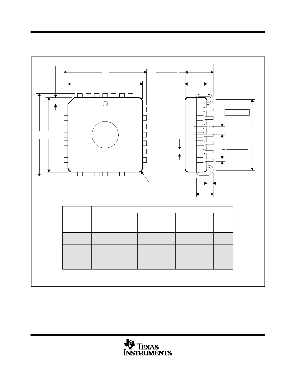
TMS370CxCx
8-BIT MICROCONTROLLER
SPNS040B ≠ NOVEMBER 1995 ≠ REVISED FEBRUARY 1997
61
POST OFFICE BOX 1443
∑
HOUSTON, TEXAS 77251≠1443
MECHANICAL DATA
FZ (S-CQCC-J**)
J-LEADED CERAMIC CHIP CARRIER
4040219 / B 03/95
0.180 (4,57)
0.140 (3,55)
C
0.020 (0,51)
0.032 (0,81)
A
B
A
B
0.025 (0,64) R TYP
0.026 (0,66)
0.120 (3,05)
0.155 (3,94)
0.014 (0,36)
0.120 (3,05)
0.040 (1,02) MIN
0.090 (2,29)
0.040 (1,02)
45
∞
A
MIN
MAX
0.485
(12,32)
(12,57)
0.495
0.455
(11,56)
(10,92)
0.430
MAX
MIN
B
C
MIN
MAX
0.410
(10,41)
(10,92)
0.430
0.630
0.610
0.630
0.655
0.695
0.685
(16,00)
(15,49)
(16,00)
(16,64)
(17,65)
(17,40)
0.740
0.680
0.730
0.765
0.795
0.785
(18,79)
(17,28)
(18,54)
(19,43)
(20,19)
(19,94)
PINS**
28
44
52
NO. OF
JEDEC
MO-087AC
MO-087AB
MO-087AA
OUTLINE
28 LEAD SHOWN
Seating Plane
(at Seating
Plane)
1
4
26
25
19
18
12
11
5
0.050 (1,27)
0.930
0.910
0.930
0.955
0.995
0.985
(23,62)
(23,11)
(23,62)
(24,26)
(25,27)
(25,02)
68
MO-087AD
NOTES: A. All linear dimensions are in inches (millimeters).
B. This drawing is subject to change without notice.
C. This package can be hermetically sealed with a ceramic lid using glass frit.
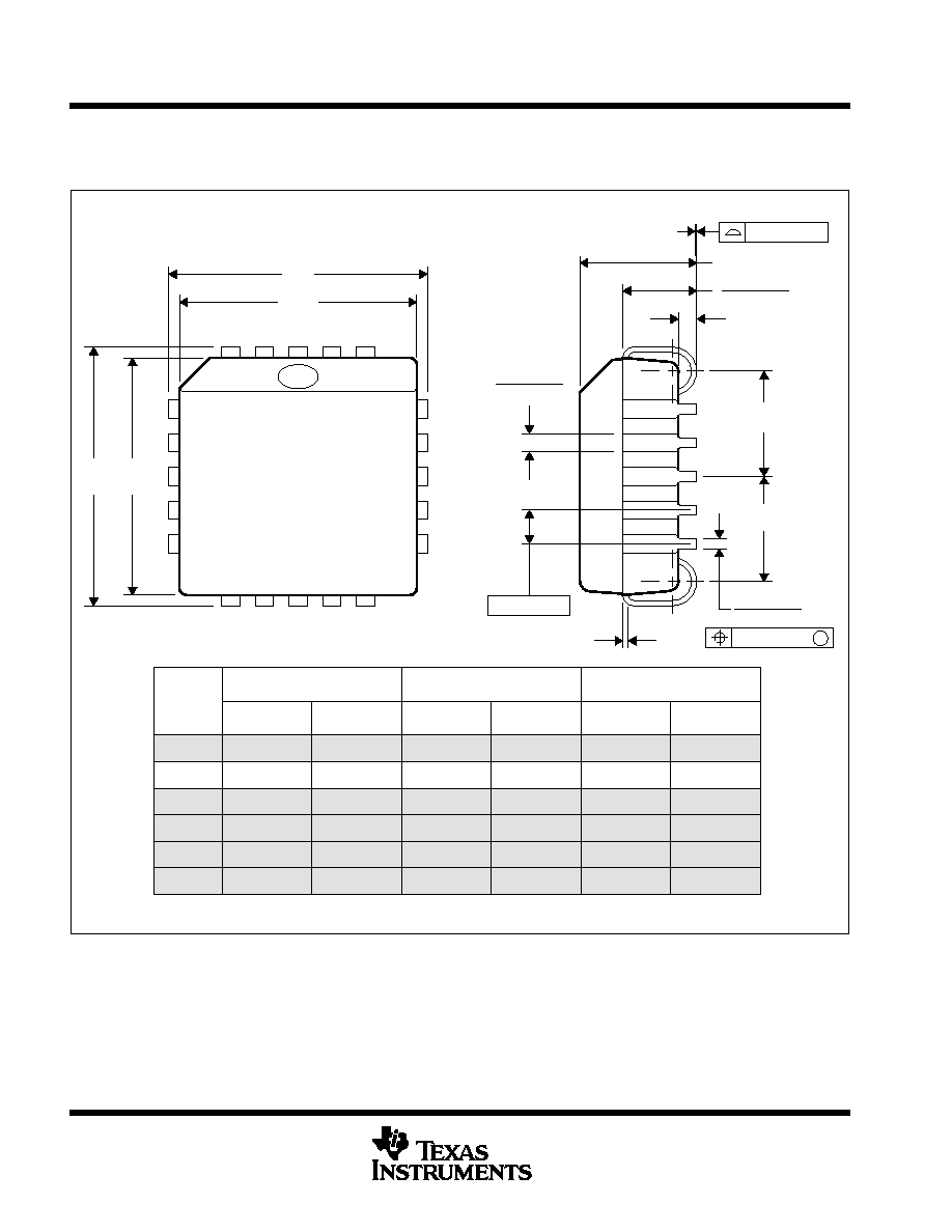
TMS370CxCx
8-BIT MICROCONTROLLER
SPNS040B ≠ NOVEMBER 1995 ≠ REVISED FEBRUARY 1997
62
POST OFFICE BOX 1443
∑
HOUSTON, TEXAS 77251≠1443
MECHANICAL DATA
FN (S-PQCC-J**)
PLASTIC J-LEADED CHIP CARRIER
4040005 / B 03/95
20 PIN SHOWN
0.026 (0,66)
0.032 (0,81)
D2 / E2
0.020 (0,51) MIN
0.180 (4,57) MAX
0.120 (3,05)
0.090 (2,29)
D2 / E2
0.013 (0,33)
0.021 (0,53)
Seating Plane
MAX
D2 / E2
0.219 (5,56)
0.169 (4,29)
0.319 (8,10)
0.469 (11,91)
0.569 (14,45)
0.369 (9,37)
MAX
0.356 (9,04)
0.456 (11,58)
0.656 (16,66)
0.008 (0,20) NOM
1.158 (29,41)
0.958 (24,33)
0.756 (19,20)
0.191 (4,85)
0.141 (3,58)
MIN
0.441 (11,20)
0.541 (13,74)
0.291 (7,39)
0.341 (8,66)
18
19
14
13
D
D1
1
3
9
E1
E
4
8
MIN
MAX
MIN
PINS
**
20
28
44
0.385 (9,78)
0.485 (12,32)
0.685 (17,40)
52
68
84
1.185 (30,10)
0.985 (25,02)
0.785 (19,94)
D / E
0.395 (10,03)
0.495 (12,57)
1.195 (30,35)
0.995 (25,27)
0.695 (17,65)
0.795 (20,19)
NO. OF
D1 / E1
0.350 (8,89)
0.450 (11,43)
1.150 (29,21)
0.950 (24,13)
0.650 (16,51)
0.750 (19,05)
0.004 (0,10)
M
0.007 (0,18)
0.050 (1,27)
NOTES: A. All linear dimensions are in inches (millimeters).
B. This drawing is subject to change without notice.
C. Falls within JEDEC MS-018

IMPORTANT NOTICE
Texas Instruments and its subsidiaries (TI) reserve the right to make changes to their products or to discontinue
any product or service without notice, and advise customers to obtain the latest version of relevant information
to verify, before placing orders, that information being relied on is current and complete. All products are sold
subject to the terms and conditions of sale supplied at the time of order acknowledgement, including those
pertaining to warranty, patent infringement, and limitation of liability.
TI warrants performance of its semiconductor products to the specifications applicable at the time of sale in
accordance with TI's standard warranty. Testing and other quality control techniques are utilized to the extent
TI deems necessary to support this warranty. Specific testing of all parameters of each device is not necessarily
performed, except those mandated by government requirements.
CERTAIN APPLICATIONS USING SEMICONDUCTOR PRODUCTS MAY INVOLVE POTENTIAL RISKS OF
DEATH, PERSONAL INJURY, OR SEVERE PROPERTY OR ENVIRONMENTAL DAMAGE ("CRITICAL
APPLICATIONS"). TI SEMICONDUCTOR PRODUCTS ARE NOT DESIGNED, AUTHORIZED, OR
WARRANTED TO BE SUITABLE FOR USE IN LIFE-SUPPORT DEVICES OR SYSTEMS OR OTHER
CRITICAL APPLICATIONS. INCLUSION OF TI PRODUCTS IN SUCH APPLICATIONS IS UNDERSTOOD TO
BE FULLY AT THE CUSTOMER'S RISK.
In order to minimize risks associated with the customer's applications, adequate design and operating
safeguards must be provided by the customer to minimize inherent or procedural hazards.
TI assumes no liability for applications assistance or customer product design. TI does not warrant or represent
that any license, either express or implied, is granted under any patent right, copyright, mask work right, or other
intellectual property right of TI covering or relating to any combination, machine, or process in which such
semiconductor products or services might be or are used. TI's publication of information regarding any third
party's products or services does not constitute TI's approval, warranty or endorsement thereof.
Copyright
©
1998, Texas Instruments Incorporated