
TPS3307 18M
TRIPLE PROCESSOR SUPERVISORS
SGLS133A - JANUARY 2003 - REVISED DECEMBER 2003
1
POST OFFICE BOX 655303
∑
DALLAS, TEXAS 75265
D
Qualified for Military Applications
D
ESD Protection Exceeds 2000 V Per
MIL-STD-883, Method 3015; Exceeds 200 V
Using Machine Model (C = 200 pF, R = 0)
D
Triple Supervisory Circuits for DSP and
Processor-Based Systems
D
Power-On Reset Generator with Fixed
Delay Time of 200 ms, No External
Capacitor Needed
D
Temperature-Compensated Voltage
Reference
D
Maximum Supply Current of 40
µ
A
D
Supply Voltage Range . . . 2 V to 6 V
D
Defined RESET
Output from V
DD
1.1 V
D
CDIP-8 and LCCC-20 Packages
D
Temperature Range . . . -55
∞
C to 125
∞
C
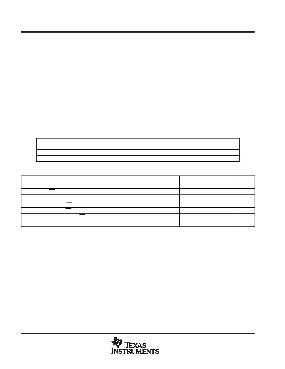
typical applications
Figure 1 lists some of the typical applications for
the TPS3307 family, and a schematic diagram for
a processor-based system application. This
application uses TI part numbers TPS3307-18
and SMJ320C6201B.
SENSE 1
SENSE 2
RESET
TPS3307-18
SENSE 3
VDD
GND
100 nF
RESET
VDD
GND
1.8 V
3.3 V
2.5 V
470 k
620 k
∑
Military applications using DSPs,
Microcontrollers or Microprocessors
w
Industrial Equipment
w
Programmable Controls
Figure 1. Applications Using the TPS3307-18
SMJ320C6201B
description
The TPS3307-18 is a micropower supply voltage supervisor designed for circuit initialization primarily in
automotive DSP and processor-based systems, which require more than one supply voltage.
The TPS3307-18 is designed for monitoring three independent supply voltages: 3.3 V/1.8 V/adj,. The adjustable
SENSE input allows the monitoring of any supply voltage >1.25 V.
Copyright
2003, Texas Instruments Incorporated
PRODUCTION DATA information is current as of publication date.
Products conform to specifications per the terms of Texas Instruments
standard warranty. Production processing does not necessarily include
testing of all parameters.
Please be aware that an important notice concerning availability, standard warranty, and use in critical applications of
Texas Instruments semiconductor products and disclaimers thereto appears at the end of this data sheet.
1
2
3
4
8
7
6
5
SENSE1
SENSE2
SENSE3
GND
V
DD
MR
RESET
RESET
JG PACKAGE
(TOP VIEW)
19
20
1
3
2
17
18
16
15
14
13
12
11
9
10
5
4
6
7
8
NC
MR
NC
RESET
NC
NC
SENSE2
NC
SENSE3
NC
NC
SENSE1
NC
V
NC
GND
NC
RESET
NC
NC
FK PACKAGE
(TOP VIEW)
NC - No internal connection
DD
On products compliant to MIL PRF 38535, all parameters are tested
unless otherwise noted. On all other products, production
processing does not necessarily include testing of all parameters.

TPS3307 18M
TRIPLE PROCESSOR SUPERVISORS
SGLS133A - JANUARY 2003 - REVISED DECEMBER 2003
2
POST OFFICE BOX 655303
∑
DALLAS, TEXAS 75265
description (continued)
The various supply voltage supervisors are designed to monitor the nominal supply voltage as shown in the
following supply voltage monitoring table.
SUPPLY VOLTAGE MONITORING
DEVICE
NOMINAL SUPERVISED VOLTAGE
THRESHOLD VOLTAGE (TYP)
DEVICE
SENSE1
SENSE2
SENSE3
SENSE1
SENSE2
SENSE3
TPS3307-18
3.3 V
1.8 V
User defined
2.93 V
1.68 V
1.25 V
The actual sense voltage has to be adjusted by an external resistor divider according to the application requirements.
During power-on, RESET is asserted when the supply voltage V
DD
becomes higher than 1.1 V. Thereafter, the
supply voltage supervisor monitors the SENSEn inputs
and keeps RESET active as long as SENSEn
remain
below the threshold voltage V
IT+
.
An internal timer delays the return of the RESET output to the inactive state (high) to ensure proper system reset.
The delay time, t
d typ
= 200 ms, starts after all SENSEn inputs
have risen above the threshold voltage V
IT+
. When
the voltage at any SENSE input drops below the threshold voltage V
IT≠
, the RESET output becomes active (low)
again.
The TPS3307-18 incorporates a manual reset input, MR. A low level at MR causes RESET to become active.
In addition to the active-low RESET output, the TPS3307-18 includes an active-high RESET output.
ORDERING INFORMATION
TA
PACKAGE
ORDERABLE
PART NUMBER
TOP-SIDE
MARKING
-55
∞
C to 125
∞
C
Ceramic Dual In Line (JG)
TPS3307-18MJGB
TPS3307-18MJGB
-55
∞
C to 125
∞
C
Leadless Ceramic Chip Carrier (FK)
TPS3307-18MFKB
TPS3307-18MFKB
Package drawings, standard packing quantities, thermal data, symbolization, and PCB design guidelines are
available at www.ti.com/sc/package.
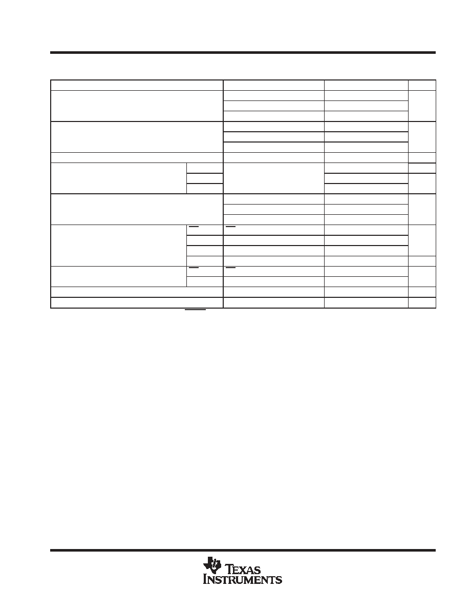
FUNCTION/TRUTH TABLES
MR
SENSE1>VIT1
SENSE2>VIT2
SENSE3>VIT3
RESET
RESET
L
X
X
X
L
H
H
0
0
0
L
H
H
0
0
1
L
H
H
0
1
0
L
H
H
0
1
1
L
H
H
1
0
0
L
H
H
1
0
1
L
H
H
1
1
0
L
H
H
1
1
1
H
L
X = Don't care

TPS3307 18M
TRIPLE PROCESSOR SUPERVISORS
SGLS133A - JANUARY 2003 - REVISED DECEMBER 2003
3
POST OFFICE BOX 655303
∑
DALLAS, TEXAS 75265
functional block diagram
_
+
_
+
_
+
R4
R2
R1
R3
Reference
Voltage
of 1.25 V
RESET
Logic + Timer
Oscillator
14 k
VDD
MR
SENSE 1
SENSE 2
GND
SENSE 3
RESET
RESET
TPS3307
timing diagram
td
td
td
RESET Because of SENSE Below VIT
RESET Because of MR
RESET Because of SENSE Below VIT-
RESET Because of SENSE Below VIT-
SENSEn
V(nom)
VIT-
MR
1
0
1
0
RESET
t
t
t
TPS3307 18M
TRIPLE PROCESSOR SUPERVISORS
SGLS133A - JANUARY 2003 - REVISED DECEMBER 2003
4
POST OFFICE BOX 655303
∑
DALLAS, TEXAS 75265
absolute maximum ratings over operating free-air temperature range (unless otherwise noted)
Supply voltage, V
DD
(see Note1)
7 V
. . . . . . . . . . . . . . . . . . . . . . . . . . . . . . . . . . . . . . . . . . . . . . . . . . . . . . . . . . . . .
All other pins (see Note 1)
-0.3 V to 7 V
. . . . . . . . . . . . . . . . . . . . . . . . . . . . . . . . . . . . . . . . . . . . . . . . . . . . . . . . . .
Maximum low output current, I
OL
5
mA
. . . . . . . . . . . . . . . . . . . . . . . . . . . . . . . . . . . . . . . . . . . . . . . . . . . . . . . . . . .
Maximum high output current, I
OH
-5
mA
. . . . . . . . . . . . . . . . . . . . . . . . . . . . . . . . . . . . . . . . . . . . . . . . . . . . . . . . .
Input clamp current, I
IK
(V
I
< 0 or V
I
> V
DD
)
±
20 mA
. . . . . . . . . . . . . . . . . . . . . . . . . . . . . . . . . . . . . . . . . . . . . . . .
Output clamp current, I
OK
(V
O
< 0 or V
O
> V
DD
)
±
20 mA
. . . . . . . . . . . . . . . . . . . . . . . . . . . . . . . . . . . . . . . . . . . .
Continuous total power dissipation
See Dissipation Rating Table
. . . . . . . . . . . . . . . . . . . . . . . . . . . . . . . . . . . . .
Operating free-air temperature range, T
A
-55
∞
C to 125
∞
C
. . . . . . . . . . . . . . . . . . . . . . . . . . . . . . . . . . . . . . . . . . .
Storage temperature range, T
stg
-65
∞
C to 150
∞
C
. . . . . . . . . . . . . . . . . . . . . . . . . . . . . . . . . . . . . . . . . . . . . . . . . . .
Soldering temperature
260
_
C
. . . . . . . . . . . . . . . . . . . . . . . . . . . . . . . . . . . . . . . . . . . . . . . . . . . . . . . . . . . . . . . . . . . .
Stresses beyond those listed under "absolute maximum ratings" may cause permanent damage to the device. These are stress ratings only, and
functional operation of the device at these or any other conditions beyond those indicated under "recommended operating conditions" is not
implied. Exposure to absolute-maximum-rated conditions for extended periods may affect device reliability.
NOTE 1: All voltage values are with respect to GND. For reliable operation the device must not be operated at 7 V for more than t = 1000 h
continuously.
DISSIPATION RATING TABLE
PACKAGE
TA
25
∞
C
POWER RATING
DERATING FACTOR
ABOVE TA = 25
∞
C
TA = 70
∞
C
POWER RATING
TA = 85
∞
C
POWER RATING
TA = 125
∞
C
POWER RATING
JG
1 W
6.25 mW/
∞
C
719 mW
625 mW
375 mW
FK
1.39 W
11.58 mW/
∞
C
869 mW
695 mW
232 mW
recommended operating conditions at specified temperature range
MIN
MAX
UNIT
Supply voltage, VDD
2
6
V
Input voltage at MR and SENSE3, VI
0
VDD+0.3
V
Input voltage at SENSE1 and SENSE2, VI
0
(VDD+0.3)VIT/1.25V
V
High-level input voltage at MR, VIH
0.7xVDD
V
Low-level input voltage at MR, VIL
0.3
◊
VDD
V
Input transition rise and fall rate at MR,
t/
V
50
ns/V
Operating free-air temperature range, TA
-55
125
∞
C
TPS3307 18M
TRIPLE PROCESSOR SUPERVISORS
SGLS133A - JANUARY 2003 - REVISED DECEMBER 2003
5
POST OFFICE BOX 655303
∑
DALLAS, TEXAS 75265
electrical characteristics over recommended operating free-air temperature range (unless
otherwise noted)
PARAMETER
TEST CONDITIONS
MIN
TYP
MAX
UNIT
VDD = 2 V to 6 V,
IOH = -20
µ
A
VDD≠ 0.2V
VOH
High-level output voltage
VDD = 3.3 V,
IOH = -2 mA
VDD≠ 0.4V
V
VOH
High-level output voltage
VDD = 6 V,
IOH = -3 mA
VDD≠ 0.4V
V
VDD = 2 V to 6 V,
IOL = 20
µ
A
0.2
VOL
Low-level output voltage
VDD = 3.3 V,
IOL = 2 mA
0.4
V
VOL
Low-level output voltage
VDD = 6 V,
IOL = 3 mA
0.4
Power-up reset voltage (see Note 2)
VDD
1.1 V,
IOL = 20
µ
A
0.4
V
Negative-going input threshold voltage
VSENSE3
1.22
1.25
1.29
V
VIT-
Negative-going input threshold voltage
(see Note 3)
VSENSE2
VDD = 2 V to 6 V
1.64
1.68
1.73
V
VIT-
(see Note 3)
VSENSE1
VDD = 2 V to 6 V
2.86
2.93
3.02
V
VIT- = 1.25 V
2
10
30
Vhys
Hysteresis at VSENSEn input
VIT- = 1.68 V
2
15
40
mV
Vhys
Hysteresis at VSENSEn input
VIT- = 2.93 V
3
30
60
mV
MR
MR = 0.7
◊
VDD,
VDD = 6 V
-130
-180
IH
High-level input current
SENSE1
VSENSE1 = VDD = 6 V
5
8
µ
A
IH
High-level input current
SENSE2
VSENSE2 = VDD = 6 V
6
9
µ
A
SENSE3
VSENSE3 = VDD
-25
25
nA
IL
Low-level input current
MR
MR = 0 V,
VDD = 6 V
-430
-600
A
IL
Low-level input current
SENSEn
VSENSE1,2,3 = 0 V
-1
1
µ
A
IDD
Supply current
40
µ
Ci
Input capacitance
VI = 0 V to VDD
10
pF
NOTES:
2. The lowest supply voltage at which RESET becomes active. tr, VDD
15
µ
s/V
3. To ensure best stability of the threshold voltage, a bypass capacitor (ceramic 0.1
µ
F) should be placed close to the supply terminals.