TPS76515, TPS76518, TPS76525, TPS76527
TPS76528, TPS76530, TPS76533, TPS76550, TPS76501
ULTRA-LOW QUIESCIENT CURRENT 150-mA LOW-DROPOUT VOLTAGE REGULATORS
SLVS236 ≠ AUGUST 1999
1
POST OFFICE BOX 655303
∑
DALLAS, TEXAS 75265
D
150-mA Low-Dropout Voltage Regulator
D
Available in 1.5-V, 1.8-V, 2.5-V, 2.7-V, 2.8-V,
3.0-V, 3.3-V, 5.0-V Fixed Output and
Adjustable Versions
D
Dropout Voltage to 85 mV (Typ) at 150 mA
(TPS76550)
D
Ultra-Low 35-
µ
A Typical Quiescent Current
D
3% Tolerance Over Specified Conditions for
Fixed-Output Versions
D
Open Drain Power Good
D
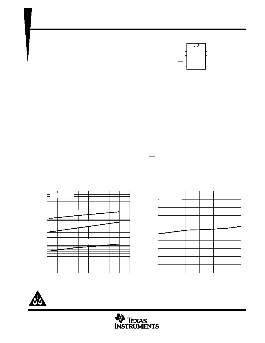
8-Pin SOIC Package
D
Thermal Shutdown Protection
description
This device is designed to have an ultra-low quiescent current and be stable with a 4.7-
µ
F capacitor. This
combination provides high performance at a reasonable cost.
Because the PMOS device behaves as a low-value resistor, the dropout voltage is very low (typically 85 mV
at an output current of 150 mA for the TPS76550) and is directly proportional to the output current. Additionally,
since the PMOS pass element is a voltage-driven device, the quiescent current is very low and independent
of output loading (typically 35
µ
A over the full range of output current, 0 mA to 150 mA). These two key
specifications yield a significant improvement in operating life for battery-powered systems. This LDO family
also features a sleep mode; applying a TTL high signal to EN (enable) shuts down the regulator, reducing the
quiescent current to less than 1
µ
A (typ).
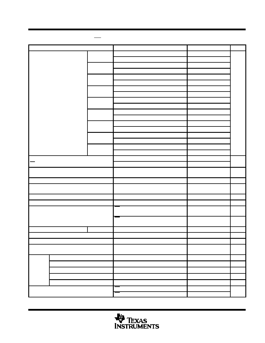
TA ≠ Free-Air Temperature ≠
∞
C
≠ Output V
oltage ≠ V
V
DO
TPS76533
DROPOUT VOLTAGE
vs
FREE-AIR TEMPERATURE
1
10
≠50
≠25
0
25
50
75
100
125
150
VI = 3.2 V
IO = 10 mA
IO = 50 mA
IO = 150 mA
100
10≠1
10≠2
10≠3
34.0
34.1
34.2
34.3
34.4
34.5
34.6
34.7
34.8
34.9
35.0
0
25
50
75
100
125
150
IL ≠ Load Current ≠ mA
TPS76533
GROUND CURRENT
vs
LOAD CURRENT
VO = 3.3 V
TA = 25
∞
C
GNDI
≠
Ground Current ≠
A
µ
Please be aware that an important notice concerning availability, standard warranty, and use in critical applications of
Texas Instruments semiconductor products and disclaimers thereto appears at the end of this data sheet.
PRODUCTION DATA information is current as of publication date.
Products conform to specifications per the terms of Texas Instruments
standard warranty. Production processing does not necessarily include
testing of all parameters.
Copyright
©
1999, Texas Instruments Incorporated
1
2
3
4
8
7
6
5
NC/FB
PG
GND
EN
OUT
OUT
IN
IN
D PACKAGE
(TOP VIEW)
TPS76515, TPS76518, TPS76525, TPS76527
TPS76528, TPS76530, TPS76533, TPS76550, TPS76501
ULTRA-LOW QUIESCIENT CURRENT 150-mA LOW-DROPOUT VOLTAGE REGULATORS
SLVS236 ≠ AUGUST 1999
2
POST OFFICE BOX 655303
∑
DALLAS, TEXAS 75265
description (continued)
Power good (PG) is an active high output, which can be used to implement a power-on reset or a low-battery
indicator.
The TPS765xx is offered in 1.5-V, 1.8-V, 2.5-V, 2.7-V, 2.8-V, 3.0-V, 3.3-V and 5.0-V fixed-voltage versions and
in an adjustable version (programmable over the range of 1.25 V to 5.5 V). Output voltage tolerance is specified
as a maximum of 3% over line, load, and temperature ranges. The TPS765xx family is available in 8 pin SOIC
package.
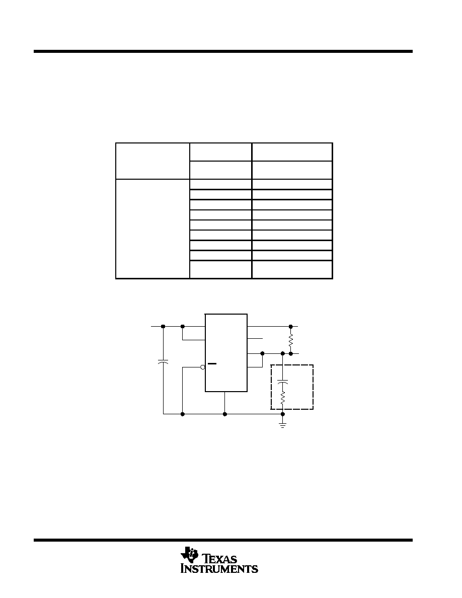
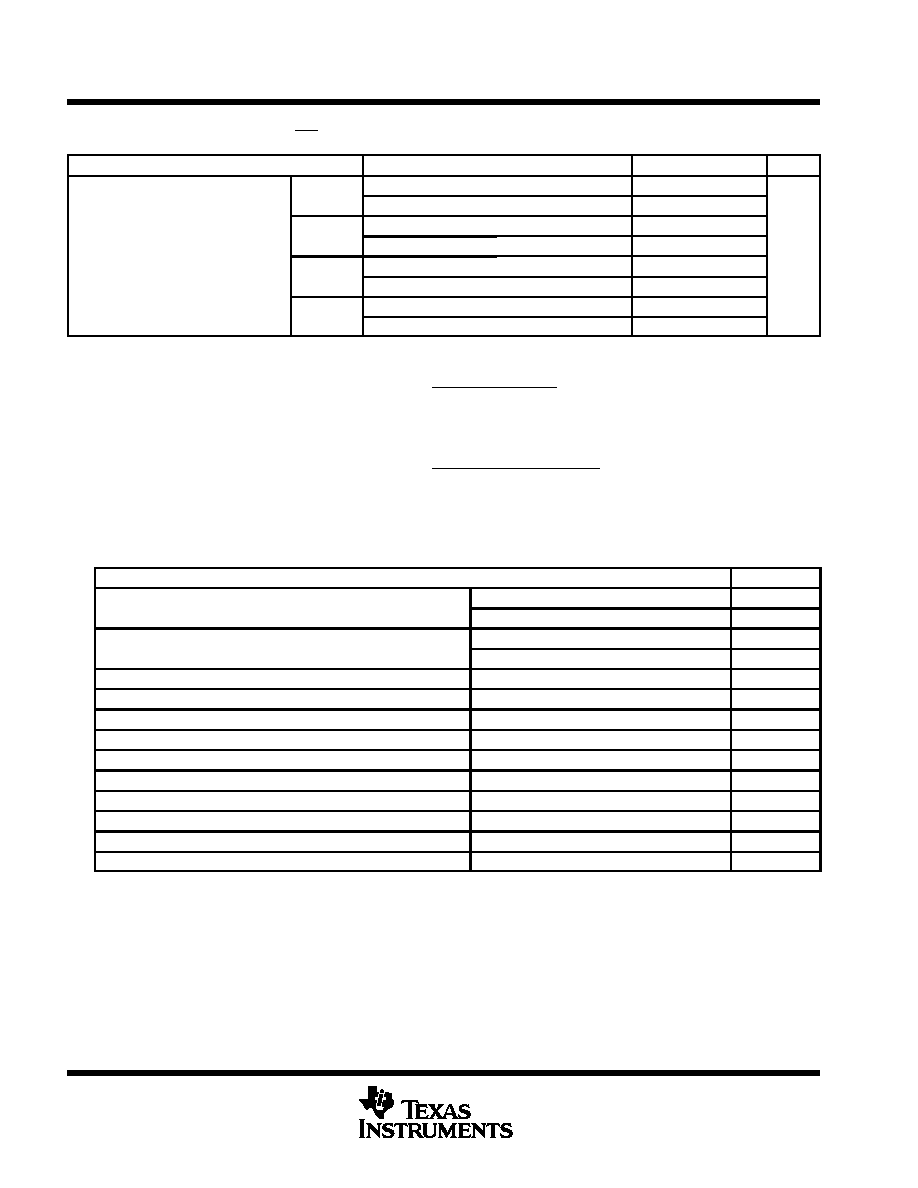
AVAILABLE OPTIONS
TJ
OUTPUT VOLTAGE
(V)
PACKAGED DEVICES
TJ
TYP
SOIC
(D)
5.0
TPS76550D
3.3
TPS76533D
3.0
TPS76530D
2.8
TPS76528D
≠ 40
∞
C to 125
∞
C
2.7
TPS76527D
≠ 40 C to 125 C
2.5
TPS76525D
1.8
TPS76518D
1.5
TPS76515D
Adjustable
1.25 V to 5.5 V
TPS76501D
The TPS76501 is programmable using an external resistor divider (see application
information). The D package is available taped and reeled. Add an R suffix to the
device type (e.g., TPS76501DR).
See application information section for capacitor selection details.
PG
OUT
OUT
6
5
4
IN
IN
EN
GND
3
2
7
8
VI
0.1
µ
F
PG
VO
4.7
µ
F
+
TPS765xx
CO
1
NC/FB
300 m
Figure 1. Typical Application Configuration for Fixed Output Options
TPS76515, TPS76518, TPS76525, TPS76527
TPS76528, TPS76530, TPS76533, TPS76550, TPS76501
ULTRA-LOW QUIESCIENT CURRENT 150-mA LOW-DROPOUT VOLTAGE REGULATORS
SLVS236 ≠ AUGUST 1999
3
POST OFFICE BOX 655303
∑
DALLAS, TEXAS 75265
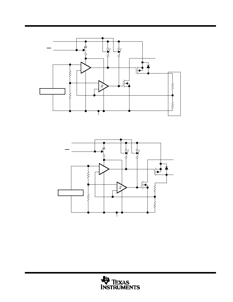
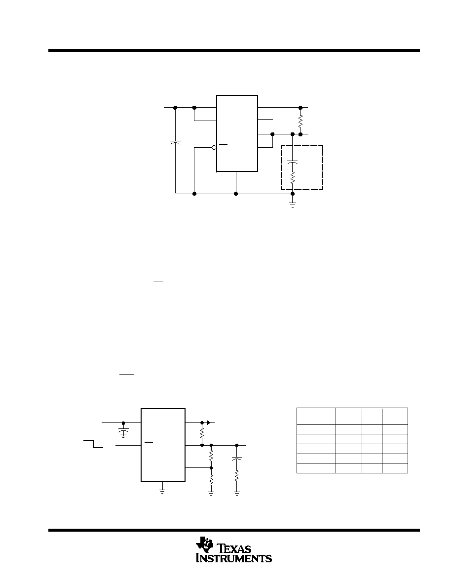
functional block diagram--adjustable version
_
+
Vref = 1.224 V
OUT
FB/NC
EN
GND
PG
_
+
IN
External to the device
R1
R2
functional block diagram--fixed-voltage version
_
+
Vref = 1.224 V
OUT
EN
GND
R1
R2
_
+
IN
PG
TPS76515, TPS76518, TPS76525, TPS76527
TPS76528, TPS76530, TPS76533, TPS76550, TPS76501
ULTRA-LOW QUIESCIENT CURRENT 150-mA LOW-DROPOUT VOLTAGE REGULATORS
SLVS236 ≠ AUGUST 1999
4
POST OFFICE BOX 655303
∑
DALLAS, TEXAS 75265
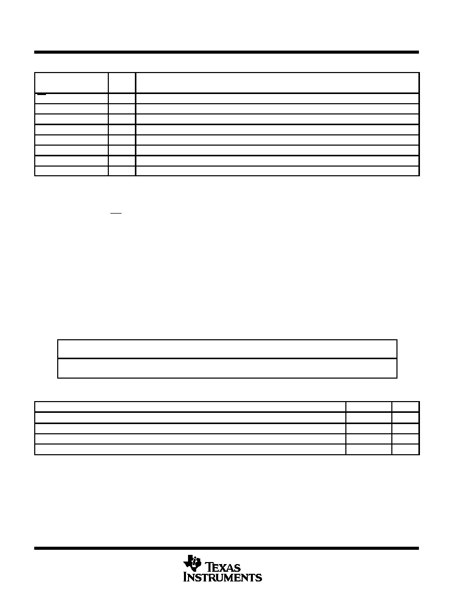
Terminal Functions ≠ SOIC Package
TERMINAL
I/O
DESCRIPTION
NAME
NO.
I/O
DESCRIPTION
EN
4
I
Enable input
FB/NC
1
I
Feedback input voltage for adjustable device (no connect for fixed options)
GND
3
Regulator ground
IN
5
I
Input voltage
IN
6
I
Input voltage
OUT
7
O
Regulated output voltage
OUT
8
O
Regulated output voltage
PG
2
O
PG output
absolute maximum ratings over operating free-air temperature range (unless otherwise noted)
Input voltage range
, V
I
≠ 0.3 V to 13.5 V
. . . . . . . . . . . . . . . . . . . . . . . . . . . . . . . . . . . . . . . . . . . . . . . . . . . . . . . . . .
Voltage range at EN
≠0.3 V to 16.5 V
. . . . . . . . . . . . . . . . . . . . . . . . . . . . . . . . . . . . . . . . . . . . . . . . . . . . . . . . . . . . . .
Maximum PG voltage
16.5 V
. . . . . . . . . . . . . . . . . . . . . . . . . . . . . . . . . . . . . . . . . . . . . . . . . . . . . . . . . . . . . . . . . . . . .
Peak output current
Internally limited
. . . . . . . . . . . . . . . . . . . . . . . . . . . . . . . . . . . . . . . . . . . . . . . . . . . . . . . . . . . . . .
Continuous total power dissipation
See dissipation rating tables
. . . . . . . . . . . . . . . . . . . . . . . . . . . . . . . . . . . . . .
Output voltage, V
O
(OUT, FB)
7 V
. . . . . . . . . . . . . . . . . . . . . . . . . . . . . . . . . . . . . . . . . . . . . . . . . . . . . . . . . . . . . . . .
Operating virtual junction temperature range, T
J
≠ 40
∞
C to 125
∞
C
. . . . . . . . . . . . . . . . . . . . . . . . . . . . . . . . . . . . .
Storage temperature range, T
stg
≠ 65
∞
C to 150
∞
C
. . . . . . . . . . . . . . . . . . . . . . . . . . . . . . . . . . . . . . . . . . . . . . . . . . .
ESD rating, HBM
2 kV
. . . . . . . . . . . . . . . . . . . . . . . . . . . . . . . . . . . . . . . . . . . . . . . . . . . . . . . . . . . . . . . . . . . . . . . . . .
Stresses beyond those listed under "absolute maximum ratings" may cause permanent damage to the device. These are stress ratings only, and
functional operation of the device at these or any other conditions beyond those indicated under "recommended operating conditions" is not
implied. Exposure to absolute-maximum-rated conditions for extended periods may affect device reliability.
All voltage values are with respect to network terminal ground.
DISSIPATION RATING TABLE 1 ≠ FREE-AIR TEMPERATURES
PACKAGE
AIR FLOW
(CFM)
TA < 25
∞
C
POWER RATING
DERATING FACTOR
ABOVE TA = 25
∞
C
TA = 70
∞
C
POWER RATING
TA = 85
∞
C
POWER RATING
D
0
568 mW
5.68 mW/
∞
C
312 mW
227 mW
D
250
904 mW
9.04 mW/
∞
C
497 mW
361 mW
recommended operating conditions
MIN
MAX
UNIT
Input voltage, VI
k
2.7
10
V
Output voltage range, VO
1.2
5.5
V
Output current, IO (Note 1)
0
150
mA
Operating virtual junction temperature, TJ (Note 1)
≠ 40
125
∞
C
k
To calculate the minimum input voltage for your maximum output current, use the following equation: VI(min) = VO(max) + VDO(max load).
NOTE 1: Continuous current and operating junction temperature are limited by internal protection circuitry, but it is not recommended that the
device operate under conditions beyond those specified in this table for extended periods of time.
TPS76515, TPS76518, TPS76525, TPS76527
TPS76528, TPS76530, TPS76533, TPS76550, TPS76501
ULTRA-LOW QUIESCIENT CURRENT 150-mA LOW-DROPOUT VOLTAGE REGULATORS
SLVS236 ≠ AUGUST 1999
5
POST OFFICE BOX 655303
∑
DALLAS, TEXAS 75265
electrical characteristics over recommended operating free-air temperature range,
V
i
= V
O(typ)
+ 1 V, I
O
= 10
µ
A, EN = 0 V, C
O
= 4.7
µ
F (unless otherwise noted)
PARAMETER
TEST CONDITIONS
MIN
TYP
MAX
UNIT
TPS76501
5.5 V
VO
1.25 V,
TJ = 25
∞
C
VO
TPS76501
5.5 V
VO
1.25 V,
TJ = ≠40
∞
C to 125
∞
C
0.97VO
1.03VO
TPS76515
TJ = 25
∞
C,
2.7 V < VIN < 10 V
1.5
TPS76515
TJ = ≠40
∞
C to 125
∞
C,
2.7 V < VIN < 10 V
1.455
1.545
TPS76518
TJ = 25
∞
C,
2.8 V < VIN < 10 V
1.8
TPS76518
TJ = ≠40
∞
C to 125
∞
C,
2.8 V < VIN < 10 V
1.746
1.854
TPS76525
TJ = 25
∞
C,
3.5 V < VIN < 10 V
2.5
TPS76525
TJ = ≠40
∞
C to 125
∞
C,
3.5 V < VIN < 10 V
2.425
2.575
Output voltage
(10
µ
A to 150 mA load)
TPS76527
TJ = 25
∞
C,
3.7 V < VIN < 10 V
2.7
V
(10
µ
A to 150 mA load)
(see Note 2)
TPS76527
TJ = ≠40
∞
C to 125
∞
C,
3.7 V < VIN < 10 V
2.619
2.781
V
(see Note 2)
TPS76528
TJ = 25
∞
C,
3.8 V < VIN < 10 V
2.8
TPS76528
TJ = ≠40
∞
C to 125
∞
C,
3.8 V < VIN < 10 V
2.716
2.884
TPS76530
TJ = 25
∞
C,
4.0 V < VIN < 10 V
3.0
TPS76530
TJ = ≠40
∞
C to 125
∞
C,
4.0 V < VIN < 10 V
2.910
3.090
TPS76533
TJ = 25
∞
C,
4.3 V < VIN < 10 V
3.3
TPS76533
TJ = ≠40
∞
C to 125
∞
C,
4.3 V < VIN < 10 V
3.201
3.399
TPS76550
TJ = 25
∞
C,
6.0 V < VIN < 10 V
5.0
TPS76550
TJ = ≠40
∞
C to 125
∞
C,
6.0 V < VIN < 10 V
4.850
5.150
Quiescent current (GND current)
10
µ
A < IO < 150 mA, TJ = 25
∞
C
35
µ
A
(
)
EN = 0V, (see Note 2)
IO = 150 mA,
TJ = ≠40
∞
C to 125
∞
C
50
µ
A
Output voltage line regulation (
VO/VO
)
(see Notes 2 and 3)
VO + 1 V < VI
10 V,
TJ = 25
∞
C
0.01
%/V
Load regulation
IO = 10
µ
A to 150 mA
0.3%
Output noise voltage
BW = 300 Hz to 50 kHz,
CO = 4.7
µ
F, TJ = 25
∞
C
200
µ
Vrms
Output current Limit
VO = 0 V
0.8
1.2
A
Thermal shutdown junction temperature
150
∞
C
Standby current
EN = VI,
TJ = 25
∞
C,
2.7 V < VI < 10 V
1
µ
A
Standby current
EN = VI,
TJ = ≠40
∞
C to 125
∞
C
2.7 V < VI < 10 V
10
µ
A
FB input current
TPS76501
FB = 1.5 V
2
nA
High level enable input voltage
2.0
V
Low level enable input voltage
0.8
V
Power supply ripple rejection (see Note 2)
f = 1 kHz,
CO = 4.7
µ
F,
IO = 10
µ
A,
TJ = 25
∞
C
63
dB
Minimum input voltage for valid PG
IO(PG) = 300
µ
A
1.1
V
Trip threshold voltage
VO decreasing
92
98
%VO
PG
Hysteresis voltage
Measured at VO
0.5
%VO
Output low voltage
VI = 2.7 V,
IO(PG) = 1mA
0.15
0.4
V
Leakage current
V(PG) = 5 V
1
µ
A
Input current (EN)
EN = 0 V
≠1
0
1
µ
A
Input current (EN)
EN = VI
≠1
1
µ
A
NOTE: 2. Minimum IN operating voltage is 2.7 V or VO(typ) + 1 V, whichever is greater. Maximum IN voltage 10 V.
TPS76515, TPS76518, TPS76525, TPS76527
TPS76528, TPS76530, TPS76533, TPS76550, TPS76501
ULTRA-LOW QUIESCIENT CURRENT 150-mA LOW-DROPOUT VOLTAGE REGULATORS
SLVS236 ≠ AUGUST 1999
6
POST OFFICE BOX 655303
∑
DALLAS, TEXAS 75265
electrical characteristics over recommended operating free-air temperature range,
V
i
= V
O(typ)
+ 1 V, I
O
= 10
µ
A, EN = 0 V, C
O
= 4.7
µ
F (unless otherwise noted) (continued)
PARAMETER
TEST CONDITIONS
MIN
TYP
MAX
UNIT
TPS76528
IO = 150 mA,
TJ = 25
∞
C
190
TPS76528
IO = 150 mA,
TJ = ≠40
∞
C to 125
∞
C
330
TPS76530
IO = 150 mA,
TJ = 25
∞
C
160
Dropout voltage
TPS76530
IO = 150 mA,
TJ = ≠40
∞
C to 125
∞
C
280
mV
g
(See Note 4)
TPS76533
IO = 150 mA,
TJ = 25
∞
C
140
mV
TPS76533
IO = 150 mA,
TJ = ≠40
∞
C to 125
∞
C
240
TPS76550
IO = 150 mA,
TJ = 25
∞
C
85
TPS76550
IO = 150 mA,
TJ = ≠40
∞
C to 125
∞
C
150
NOTES:
3. If VO
1.8 V then Vimin = 2.7 V, Vimax = 10 V:
Line Reg. (mV)
+
% V
V
O
V
imax
*
2.7 V
100
1000
If VO
2.5 V then Vimin = VO + 1 V, Vimax = 10 V:
Line Reg. (mV)
+
% V
V
O
V
imax
*
V
O
)
1 V
100
1000
4. IN voltage equals VO(Typ) ≠ 100 mV; TPS76501 output voltage set to 3.3 V nominal with external resistor divider. TPS76515,
TPS76518, TPS76525, and TPS76527 dropout voltage limited by input voltage range limitations (i.e., TPS76530 input voltage
needs to drop to 2.9 V for purpose of this test).
Table of Graphs
FIGURE
Output voltage
vs Load current
2, 3
Output voltage
vs Free-air temperature
4, 5
Ground current
vs Load current
6, 7
Ground current
vs Free-air temperature
8, 9
Power supply ripple rejection
vs Frequency
10
Output spectral noise density
vs Frequency
11
Output impedance
vs Frequency
12
Dropout voltage
vs Free-air temperature
13, 14
Line transient response
15, 17
Load transient response
16, 18
Output voltage
vs Time
19
Dropout voltage
vs Input voltage
20
Equivalent series resistance (ESR)
vs Output current
21 ≠ 24
Equivalent series resistance (ESR)
vs Added ceramic capacitance
25, 26
TPS76515, TPS76518, TPS76525, TPS76527
TPS76528, TPS76530, TPS76533, TPS76550, TPS76501
ULTRA-LOW QUIESCIENT CURRENT 150-mA LOW-DROPOUT VOLTAGE REGULATORS
SLVS236 ≠ AUGUST 1999
7
POST OFFICE BOX 655303
∑
DALLAS, TEXAS 75265
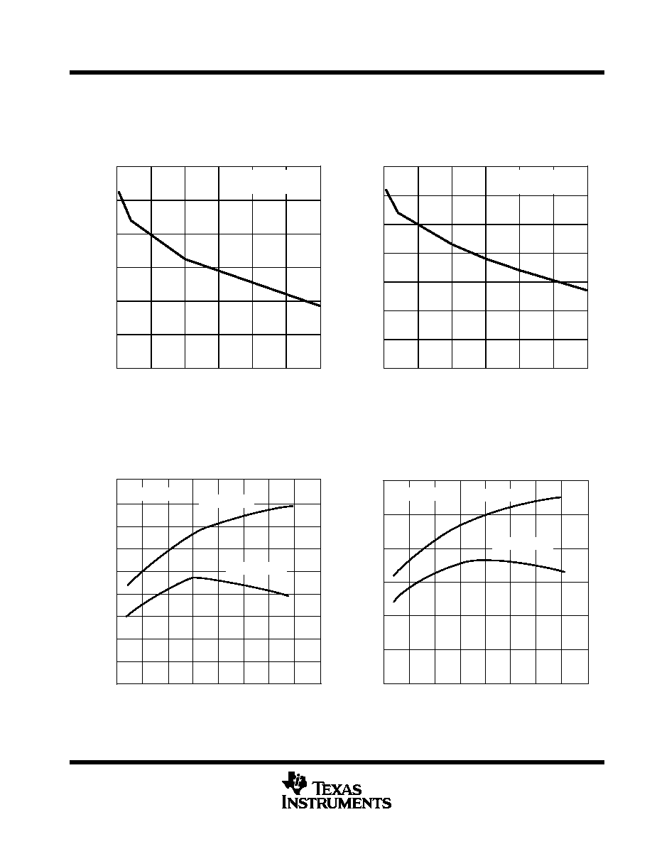
TYPICAL CHARACTERISTICS
Figure 2
IL ≠ Load Current ≠ mA
≠ Output V
oltage ≠ V
V
O
TPS76533
OUTPUT VOLTAGE
vs
LOAD CURRENT
3.292
3.294
3.296
3.298
3.300
3.302
3.304
0
25
50
75
100
125
150
VI = 4.3 V
TA = 25
∞
C
Figure 3
IL ≠ Load Current ≠ mA
≠ Output V
oltage ≠ V
V
O
TPS76515
OUTPUT VOLTAGE
vs
LOAD CURRENT
1.487
1.488
1.489
1.490
1.491
1.492
1.493
1.494
0
25
50
75
100
125
150
VI = 2.7 V
TA = 25
∞
C
Figure 4
TA ≠ Free-Air Temperature ≠
∞
C
TPS76533
OUTPUT VOLTAGE
vs
FREE-AIR TEMPERATURE
≠ Output V
oltage ≠ V
V
O
3.310
3.305
3.300
3.295
3.290
3.285
3.280
3.275
3.270
3.265
≠25
≠50
0
25
50
75
100
125
150
VI = 4.3 V
IO = 10
µ
A
IO = 150 mA
Figure 5
TA ≠ Free-Air Temperature ≠
∞
C
TPS76515
OUTPUT VOLTAGE
vs
FREE-AIR TEMPERATURE
≠ Output V
oltage ≠ V
V
O
1.505
≠50
1.500
1.495
1.490
1.485
1.480
1.475
≠25
0
25
50
75
100
125
150
VI = 2.7 V
IO = 10
µ
A
IO = 150 mA
TPS76515, TPS76518, TPS76525, TPS76527
TPS76528, TPS76530, TPS76533, TPS76550, TPS76501
ULTRA-LOW QUIESCIENT CURRENT 150-mA LOW-DROPOUT VOLTAGE REGULATORS
SLVS236 ≠ AUGUST 1999
8
POST OFFICE BOX 655303
∑
DALLAS, TEXAS 75265
TYPICAL CHARACTERISTICS
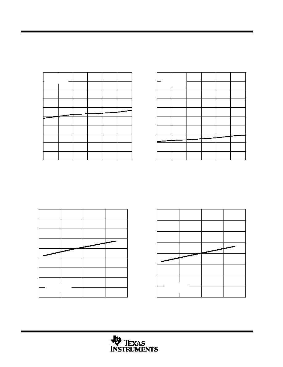
Figure 6
34.0
34.1
34.2
34.3
34.4
34.5
34.6
34.7
34.8
34.9
35.0
0
25
50
75
100
125
150
IL ≠ Load Current ≠ mA
TPS76533
GROUND CURRENT
vs
LOAD CURRENT
VO = 3.3 V
TA = 25
∞
C
GNDI
≠
Ground Current ≠
A
µ
Figure 7
33.0
33.1
33.2
33.3
33.4
33.5
33.6
33.7
33.8
33.9
34.0
0
25
50
75
100
125
150
IL ≠ Load Current ≠ mA
TPS76515
GROUND CURRENT
vs
LOAD CURRENT
VO = 1.5 V
TA = 25
∞
C
GNDI
≠
Ground Current ≠
A
µ
Figure 8
TA ≠ Free-Air Temperature ≠
∞
C
TPS76533
GROUND CURRENT
vs
FREE-AIR TEMPERATURE
10
15
20
25
30
35
40
45
50
55
≠50
0
50
100
150
VO = 3.3 V
IO = 150 mA
GNDI
≠
Ground Current ≠
A
µ
Figure 9
TA ≠ Free-Air Temperature ≠
∞
C
TPS76515
GROUND CURRENT
vs
FREE-AIR TEMPERATURE
15
20
25
30
35
40
45
50
55
≠50
0
50
100
150
VO = 1.5 V
IO = 150 mA
GNDI
≠
Ground Current ≠
A
µ
TPS76515, TPS76518, TPS76525, TPS76527
TPS76528, TPS76530, TPS76533, TPS76550, TPS76501
ULTRA-LOW QUIESCIENT CURRENT 150-mA LOW-DROPOUT VOLTAGE REGULATORS
SLVS236 ≠ AUGUST 1999
9
POST OFFICE BOX 655303
∑
DALLAS, TEXAS 75265
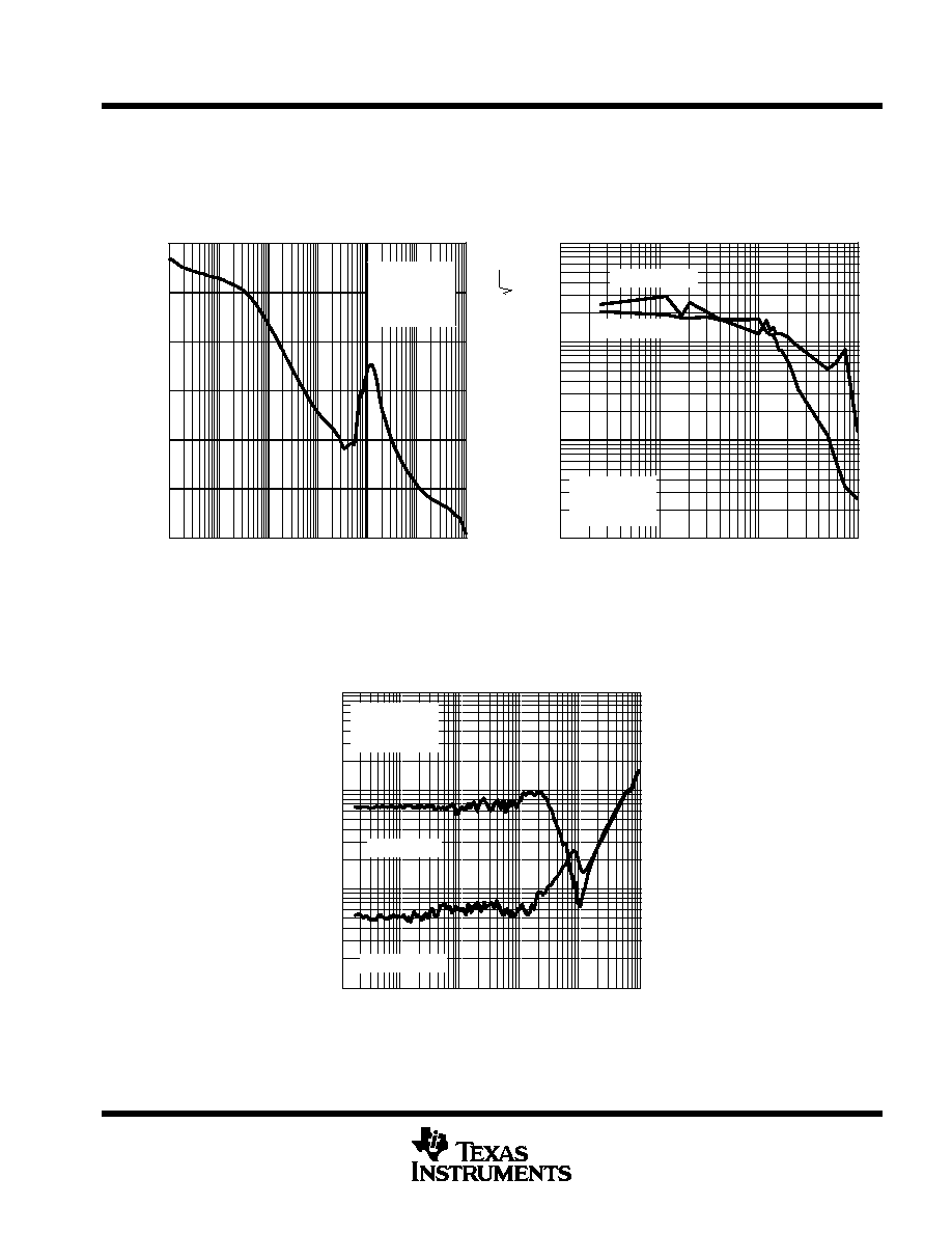
TYPICAL CHARACTERISTICS
Figure 10
f ≠ Frequency ≠ Hz
TPS76533
POWER SUPPLY RIPPLE REJECTION
vs
FREQUENCY
10
20
30
40
50
60
70
10.00
100.00 1000.0010000.00
100000.00
1000000.00
10000000.0
PSRR ≠ Power Supply Ripple Rejection ≠ dB
VI = 4.3 V
CO = 10
µ
F
IO = 150 mA
TA = 25
∞
C
10
100
1k
10k
100k
1M
10M
Figure 11
f ≠ Frequency ≠ Hz
TPS76533
OUTPUT SPECTRAL NOISE DENSITY
vs
FREQUENCY
VI = 4.3 V
CO = 10
µ
F
TA = 25
∞
C
1k
10k
100k
IO = 150 mA
IO = 1 mA
V
Hz
Output Spectral Noise Density ≠
µ
101
100
10≠1
10≠2
100
101
100
10≠1
10≠2
f ≠ Frequency ≠ Hz
TPS76533
OUTPUT IMPEDANCE
vs
FREQUENCY
VI = 4.3 V
CO = 10
µ
F
TA = 25
∞
C
10
1k
10k
1M
IO = 150 mA
IO = 1 mA
100
100k
≠ Output Impedance ≠
Z
o
Figure 12
TPS76515, TPS76518, TPS76525, TPS76527
TPS76528, TPS76530, TPS76533, TPS76550, TPS76501
ULTRA-LOW QUIESCIENT CURRENT 150-mA LOW-DROPOUT VOLTAGE REGULATORS
SLVS236 ≠ AUGUST 1999
10
POST OFFICE BOX 655303
∑
DALLAS, TEXAS 75265
TYPICAL CHARACTERISTICS
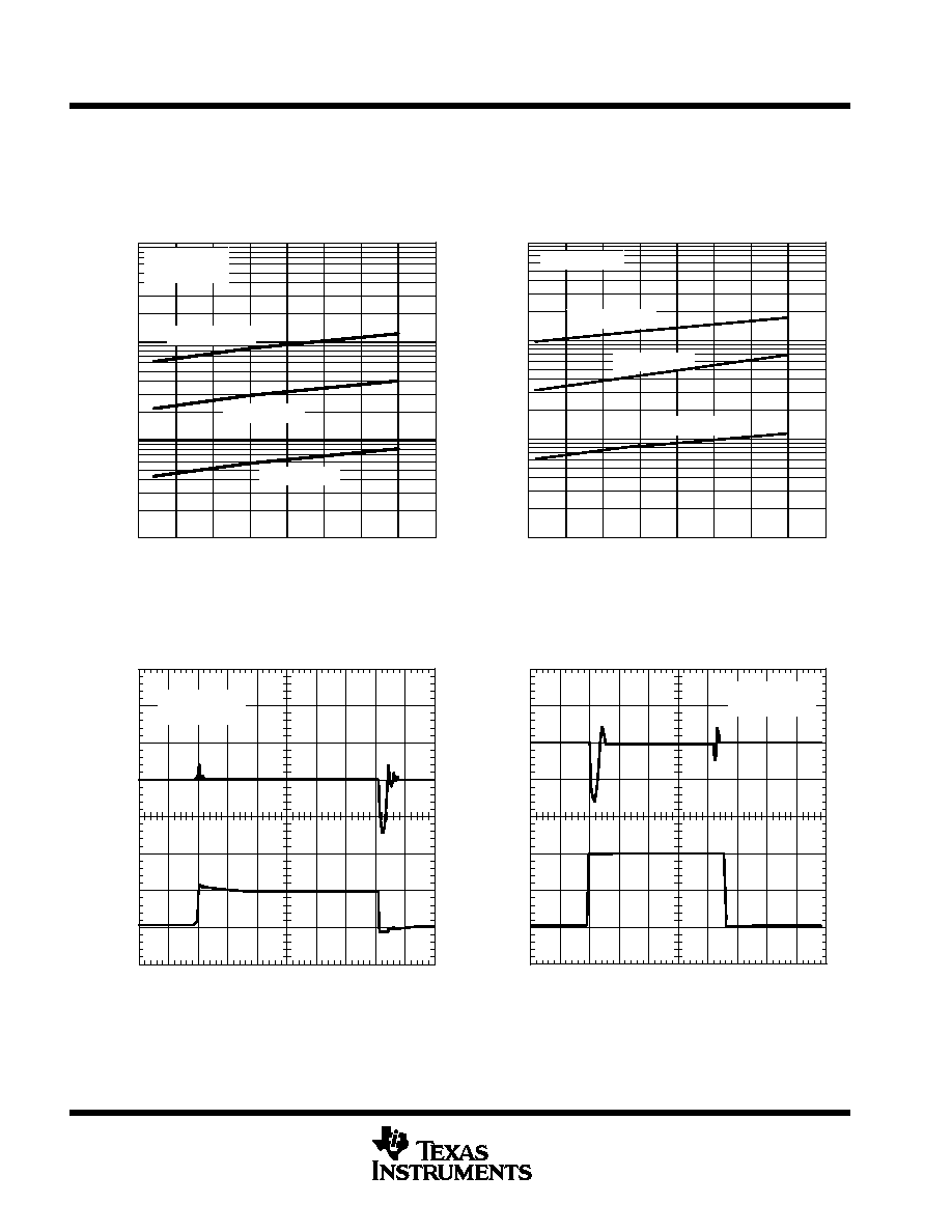
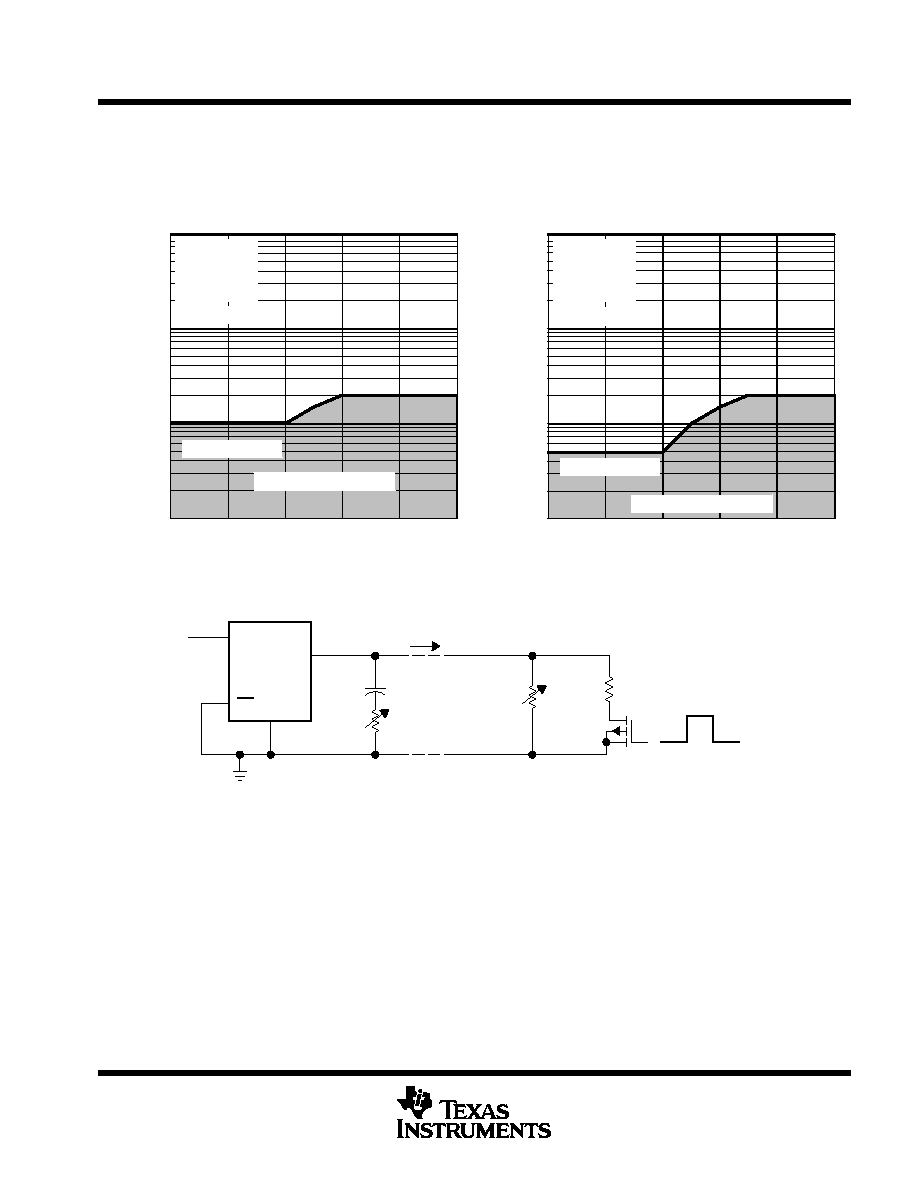
Figure 13
≠50
≠25
0
25
50
75
100
125
150
TA ≠ Free-Air Temperature ≠
∞
C
TPS76550
DROPOUT VOLTAGE
vs
FREE-AIR TEMPERATURE
100
10≠1
10≠2
10≠3
IO = 10 mA
IO = 50 mA
IO = 150 mA
VI = 4.9 V
CO = 4.7
µ
F
≠ Output V
oltage ≠ V
V
DO
Figure 14
TA ≠ Free-Air Temperature ≠
∞
C
TPS76533
DROPOUT VOLTAGE
vs
FREE-AIR TEMPERATURE
≠50
≠25
0
25
50
75
100
125
150
VI = 3.2 V
IO = 10 mA
IO = 50 mA
IO = 150 mA
100
10≠1
10≠2
10≠3
≠ Output V
oltage ≠ V
V
DO
Figure 15
V
O
≠ Change in
50
0
3.7
2.7
TPS76515
LINE TRANSIENT RESPONSE
V
I
t ≠ Time ≠
µ
s
0
300
200
100
400 500
700
600
800 900 1000
≠ Input V
oltage ≠ V
Output
V
oltage ≠ mV
CL = 4.7
µ
F
TA = 25
∞
C
≠50
100
Figure 16
t ≠ Time ≠
µ
s
TPS76515
LOAD TRANSIENT RESPONSE
I ≠ Output Current ≠ mA O
V
O
≠ Change in
Output
V
oltage ≠ mV
CL = 4.7
µ
F
TA = 25
∞
C
150
0
0
200
400
≠200
≠400
0
300
200
100
400 500
700
600
800 900 1000
TPS76515, TPS76518, TPS76525, TPS76527
TPS76528, TPS76530, TPS76533, TPS76550, TPS76501
ULTRA-LOW QUIESCIENT CURRENT 150-mA LOW-DROPOUT VOLTAGE REGULATORS
SLVS236 ≠ AUGUST 1999
11
POST OFFICE BOX 655303
∑
DALLAS, TEXAS 75265
TYPICAL CHARACTERISTICS
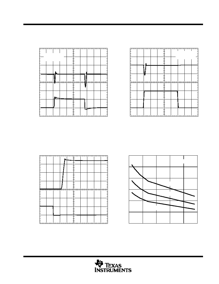
Figure 17
V
O
≠ Change in
100
50
4.3
TPS76533
LINE TRANSIENT RESPONSE
V
I
t ≠ Time ≠
µ
s
≠ Input V
oltage ≠ V
Output
V
oltage ≠ mV
CL = 4.7
µ
F
TA = 25
∞
C
0
5.3
≠100
≠50
0
300
200
100
400 500
700
600
800 900 1000
Figure 18
t ≠ Time ≠
µ
s
TPS76533
LOAD TRANSIENT RESPONSE
I ≠ Output Current ≠ mA O
V
O
≠ Change in
Output
V
oltage ≠ mV
CL = 4.7
µ
F
TA = 25
∞
C
150
0
0
200
400
≠200
0
300
200
100
400 500
700
600
800 900 1000
Figure 19
t ≠ Time ≠
µ
s
TPS76533
OUTPUT VOLTAGE
vs
TIME (AT STARTUP)
3
2
V
O
≠ Output V
oltage ≠ V
0
1
4
Enable Pulse ≠ V
0
0
300
200
100
400 500
700
600
800 900 1000
4.3
Figure 20
VI ≠ Input Voltage ≠ V
≠ Output V
oltage ≠ V
V
DO
TPS76501
DROPOUT VOLTAGE
vs
INPUT VOLTAGE
0.00
0.05
0.10
0.15
0.20
0.25
0.30
2.5
3.0
3.5
4.0
4.5
5.0
IO = 150 mA
TA = 125
∞
C
TA = 25
∞
C
TA = ≠40
∞
C
TPS76515, TPS76518, TPS76525, TPS76527
TPS76528, TPS76530, TPS76533, TPS76550, TPS76501
ULTRA-LOW QUIESCIENT CURRENT 150-mA LOW-DROPOUT VOLTAGE REGULATORS
SLVS236 ≠ AUGUST 1999
12
POST OFFICE BOX 655303
∑
DALLAS, TEXAS 75265
TYPICAL CHARACTERISTICS
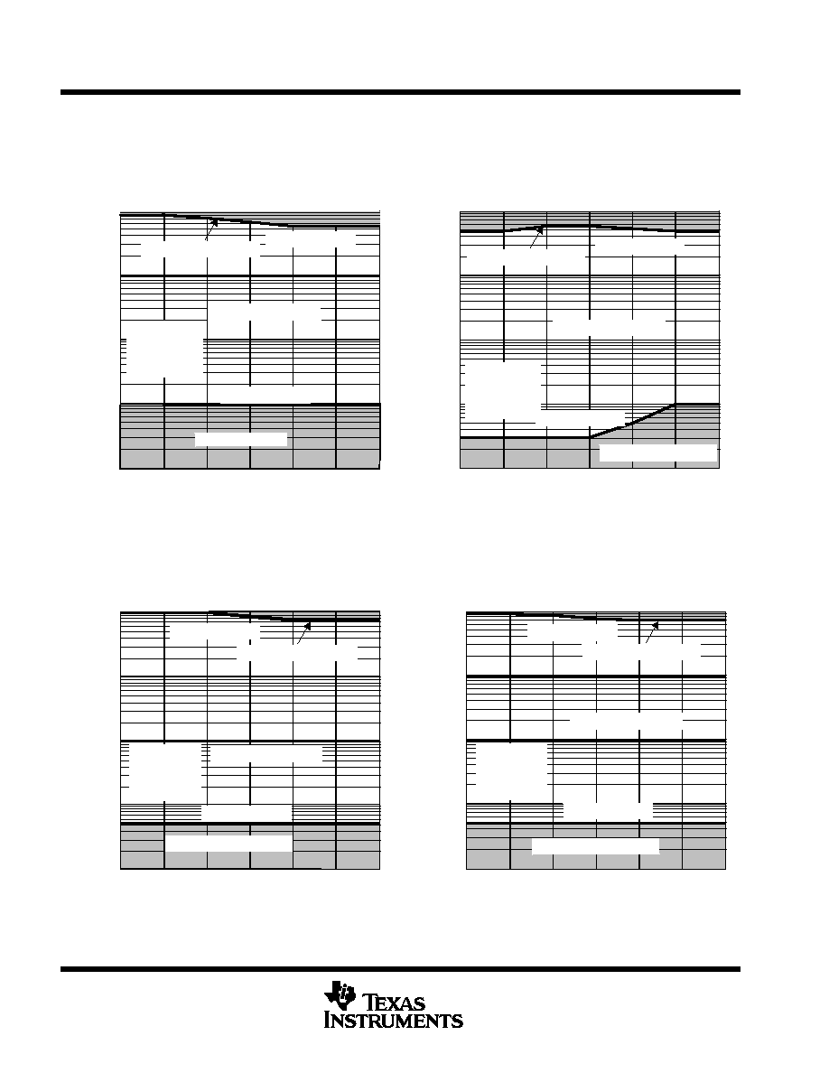
Figure 21
0.01
0.10
1.00
10.00
100.00
0
25
50
75
100
125
150
IO ≠ Output Current ≠ mA
TYPICAL REGION OF STABILITY
EQUIVALENT SERIES RESISTANCE
vs
OUTPUT CURRENT
VI = 4.3 V
CO = 4.7
µ
F
VO = 3.3 V
TA = 25
∞
C
Minimum ESR
ESR ≠ Equivalent Series Resistance ≠
Maximum ESR
Region of Stability
102
101
100
10≠1
10≠2
Region of Instability
Region of Instability
Figure 22
0.01
0.10
1.00
10.00
100.00
0
25
50
75
100
125
150
IO ≠ Output Current ≠ mA
TYPICAL REGION OF STABILITY
EQUIVALENT SERIES RESISTANCE
vs
OUTPUT CURRENT
VI = 4.3 V
CO = 4.7
µ
F
VO = 3.3 V
TA = 125
∞
C
Minimum ESR
ESR ≠ Equivalent Series Resistance ≠
Maximum ESR
Region of Stability
Region of Instability
102
101
100
10≠2
10≠1
Region of Instability
Figure 23
0.01
0.10
1.00
10.00
100.00
0
25
50
75
100
125
150
IO ≠ Output Current ≠ mA
TYPICAL REGION OF STABILITY
EQUIVALENT SERIES RESISTANCE
vs
OUTPUT CURRENT
VI = 4.3 V
CO = 10
µ
F
VO = 3.3 V
TA = 25
∞
C
Minimum ESR
ESR ≠ Equivalent Series Resistance ≠
Maximum ESR
Region of Stability
Region of Instability
102
101
100
10≠2
10≠1
Region of Instability
Figure 24
100
10≠2
0
25
50
75
100
125
150
IO ≠ Output Current ≠ mA
TYPICAL REGION OF STABILITY
EQUIVALENT SERIES RESISTANCE
vs
OUTPUT CURRENT
VI = 4.3 V
CO = 10
µ
F
VO = 3.3 V
TA = 125
∞
C
Minimum ESR
ESR ≠ Equivalent Series Resistance ≠
Maximum ESR
Region of Stability
Region of Instability
101
100
10≠1
Region of Instability
10≠2
102
Equivalent series resistance (ESR) refers to the total series resistance, including the ESR of the capacitor, any series resistance added
externally, and PWB trace resistance to CO.
TPS76515, TPS76518, TPS76525, TPS76527
TPS76528, TPS76530, TPS76533, TPS76550, TPS76501
ULTRA-LOW QUIESCIENT CURRENT 150-mA LOW-DROPOUT VOLTAGE REGULATORS
SLVS236 ≠ AUGUST 1999
13
POST OFFICE BOX 655303
∑
DALLAS, TEXAS 75265
TYPICAL CHARACTERISTICS
Figure 25
0.01
0.10
1.00
10.00
0
0.2
0.4
0.6
0.8
1.0
Added Ceramic Capacitance ≠
µ
F
TYPICAL REGION OF STABILITY
EQUIVALENT SERIES RESISTANCE
vs
ADDED CERAMIC CAPACITANCE
ESR ≠ Equivalent Series Resistance ≠
101
100
10≠1
10≠2
VI = 4.3 V
CO = 4.7
µ
F
VO = 3.3 V
TA = 25
∞
C
Minimum ESR
Region of Instability
IO = 150 mA
Figure 26
Added Ceramic Capacitance ≠
µ
F
TYPICAL REGION OF STABILITY
EQUIVALENT SERIES RESISTANCE
vs
ADDED CERAMIC CAPACITANCE
0.01
0.10
1.00
10.00
0
0.2
0.4
0.6
0.8
1.0
ESR ≠ Equivalent Series Resistance ≠
101
100
10≠1
10≠2
VI = 4.3 V
VO = 3.3 V
CO = 10
µ
F
TA = 25
∞
C
Minimum ESR
Region of Instability
101
IO = 150 mA
IN
EN
OUT
+
GND
CO
ESR
RL
VI
To Load
Figure 27. Test Circuit for Typical Regions of Stability (Figures 20 through 23) (Fixed Output Options)
Equivalent series resistance (ESR) refers to the total series resistance, including the ESR of the capacitor, any series resistance added
externally, and PWB trace resistance to CO.

TPS76515, TPS76518, TPS76525, TPS76527
TPS76528, TPS76530, TPS76533, TPS76550, TPS76501
ULTRA-LOW QUIESCIENT CURRENT 150-mA LOW-DROPOUT VOLTAGE REGULATORS
SLVS236 ≠ AUGUST 1999
14
POST OFFICE BOX 655303
∑
DALLAS, TEXAS 75265
APPLICATION INFORMATION
The TPS765xx family includes eight fixed-output voltage regulators (1.5 V, 1.8 V, 2.5 V, 2.7 V, 2.8 V, 3.0 V,
3.3 V, and 5.0 V), and an adjustable regulator, the TPS76501 (adjustable from 1.25 V to 5.5 V).
device operation
The TPS765xx features very low quiescent current, which remains virtually constant even with varying loads.
Conventional LDO regulators use a pnp pass element, the base current of which is directly proportional to the
load current through the regulator (I
B
= I
C
/
). The TPS765xx uses a PMOS transistor to pass current; because
the gate of the PMOS is voltage driven, operating current is low and invariable over the full load range.
Another pitfall associated with the pnp-pass element is its tendency to saturate when the device goes into
dropout. The resulting drop in
forces an increase in I
B
to maintain the load. During power up, this translates
to large start-up currents. Systems with limited supply current may fail to start up. In battery-powered systems,
it means rapid battery discharge when the voltage decays below the minimum required for regulation. The
TPS765xx quiescent current remains low even when the regulator drops out, eliminating both problems.
The TPS765xx family also features a shutdown mode that places the output in the high-impedance state
(essentially equal to the feedback-divider resistance) and reduces quiescent current to 1
µ
A (typ). If the
shutdown feature is not used, EN should be tied to ground. Response to an enable transition is quick; regulated
output voltage is reestablished in typically 160
µ
s.
minimum load requirements
The TPS765xx family is stable even at zero load; no minimum load is required for operation.
FB - pin connection (adjustable version only)
The FB pin is an input pin to sense the output voltage and close the loop for the adjustable option . The output
voltage is sensed through a resistor divider network to close the loop as it is shown in Figure 29. Normally, this
connection should be as short as possible; however, the connection can be made near a critical circuit to
improve performance at that point. Internally, FB connects to a high-impedance wide-bandwidth amplifier and
noise pickup feeds through to the regulator output. Routing the FB connection to minimize/avoid noise pickup
is essential.
external capacitor requirements
An input capacitor is not usually required; however, a ceramic bypass capacitor (0.047
µ
F or larger) improves
load transient response and noise rejection if the TPS765xx is located more than a few inches from the power
supply. A higher-capacitance electrolytic capacitor may be necessary if large (hundreds of milliamps) load
transients with fast rise times are anticipated.
Like all low dropout regulators, the TPS765xx requires an output capacitor connected between OUT and GND
to stabilize the internal control loop. The minimum recommended capacitance value is 4.7
µ
F and the ESR
(equivalent series resistance) must be between 300-m
and 20-
. Capacitor values 4.7
µ
F or larger are
acceptable, provided the ESR is less than 20
. Solid tantalum electrolytic, aluminum electrolytic, and multilayer
ceramic capacitors are all suitable, provided they meet the requirements described previously.
TPS76515, TPS76518, TPS76525, TPS76527
TPS76528, TPS76530, TPS76533, TPS76550, TPS76501
ULTRA-LOW QUIESCIENT CURRENT 150-mA LOW-DROPOUT VOLTAGE REGULATORS
SLVS236 ≠ AUGUST 1999
15
POST OFFICE BOX 655303
∑
DALLAS, TEXAS 75265
APPLICATION INFORMATION
external capacitor requirements (continued)
PG
OUT
OUT
6
5
4
IN
IN
EN
GND
3
2
7
8
VI
0.1
µ
F
PG
VO
4.7
µ
F
+
TPS765xx
CO
1
NC/FB
300 m
250 k
Figure 28. Typical Application Circuit (Fixed Versions)
programming the TPS76501 adjustable LDO regulator
The output voltage of the TPS76501 adjustable regulator is programmed using an external resistor divider as
shown in Figure 29. The output voltage is calculated using:
V
O
+
V
ref
1
)
R1
R2
(1)
Where
V
ref
= 1.224 V typ (the internal reference voltage)
Resistors R1 and R2 should be chosen for approximately 7-
µ
A divider current. Lower value resistors can be
used but offer no inherent advantage and waste more power. Higher values should be avoided as leakage
currents at FB increase the output voltage error. The recommended design procedure is to choose
R2 = 169 k
to set the divider current at 7
µ
A and then calculate R1 using:
R1
+
V
O
V
ref
*
1
R2
(2)
OUTPUT
VOLTAGE
R1
R2
2.5 V
3.3 V
3.6 V
4.0 V
5.0 V
UNIT
174
287
324
383
523
169
169
169
169
169
k
k
k
k
k
OUTPUT VOLTAGE
PROGRAMMING GUIDE
VO
VI
PG
OUT
FB / NC
R1
R2
GND
EN
IN
0.8 V
2.0 V
TPS76501
PG
0.1
µ
F
250 k
300 m
CO
Figure 29. TPS76501 Adjustable LDO Regulator Programming
TPS76515, TPS76518, TPS76525, TPS76527
TPS76528, TPS76530, TPS76533, TPS76550, TPS76501
ULTRA-LOW QUIESCIENT CURRENT 150-mA LOW-DROPOUT VOLTAGE REGULATORS
SLVS236 ≠ AUGUST 1999
16
POST OFFICE BOX 655303
∑
DALLAS, TEXAS 75265
APPLICATION INFORMATION
power-good indicator
The TPS765xx features a power-good (PG) output that can be used to monitor the status of the regulator. The
internal comparator monitors the output voltage: when the output drops to between 92% and 98% of its nominal
regulated value, the PG output transistor turns on, taking the signal low. The open-drain output requires a pullup
resistor. If not used, it can be left floating. PG can be used to drive power-on reset circuitry or used as a
low-battery indicator.
regulator protection
The TPS765xx PMOS-pass transistor has a built-in back diode that conducts reverse currents when the input
voltage drops below the output voltage (e.g., during power down). Current is conducted from the output to the
input and is not internally limited. When extended reverse voltage is anticipated, external limiting may be
appropriate.
The TPS765xx also features internal current limiting and thermal protection. During normal operation, the
TPS765xx limits output current to approximately 0.8 A. When current limiting engages, the output voltage scales
back linearly until the overcurrent condition ends. While current limiting is designed to prevent gross device
failure, care should be taken not to exceed the power dissipation ratings of the package. If the temperature of
the device exceeds 150
∞
C(typ), thermal-protection circuitry shuts it down. Once the device has cooled below
130
∞
C(typ), regulator operation resumes.
power dissipation and junction temperature
Specified regulator operation is assured to a junction temperature of 125
∞
C; the maximum junction temperature
should be restricted to 125
∞
C under normal operating conditions. This restriction limits the power dissipation
the regulator can handle in any given application. To ensure the junction temperature is within acceptable limits,
calculate the maximum allowable dissipation, P
D(max)
, and the actual dissipation, P
D
, which must be less than
or equal to P
D(max)
.
The maximum-power-dissipation limit is determined using the following equation:
P
D(max)
+
T
J
max
*
T
A
R
q
JA
Where
T
J
max
is the maximum allowable junction temperature
T
A
is the ambient temperature.
R
JA
is the thermal resistance junction-to-ambient for the package, i.e., 176
∞
C/W for the 8-terminal
SOIC.
The regulator dissipation is calculated using:
P
D
+
V
I
*
V
O
I
O
Power dissipation resulting from quiescent current is negligible. Excessive power dissipation will trigger the
thermal protection circuit.
TPS76515, TPS76518, TPS76525, TPS76527
TPS76528, TPS76530, TPS76533, TPS76550, TPS76501
ULTRA-LOW QUIESCIENT CURRENT 150-mA LOW-DROPOUT VOLTAGE REGULATORS
SLVS236 ≠ AUGUST 1999
17
POST OFFICE BOX 655303
∑
DALLAS, TEXAS 75265
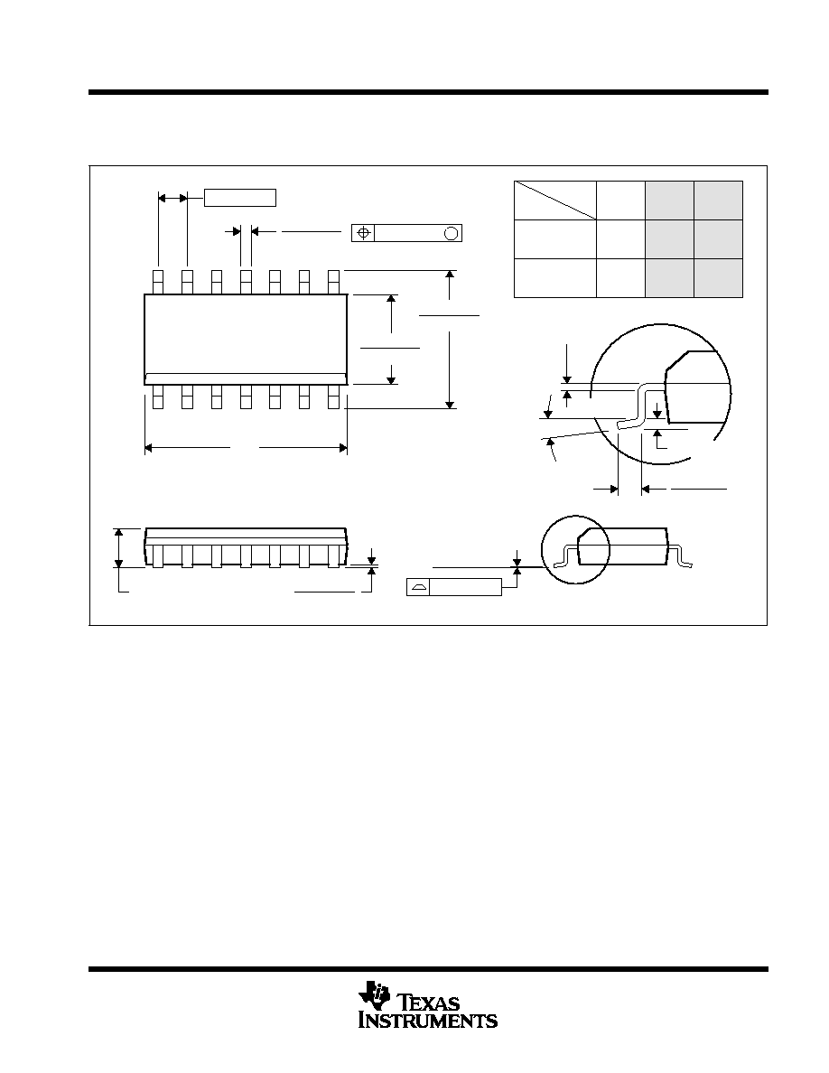
MECHANICAL DATA
D (R-PDSO-G**)
PLASTIC SMALL-OUTLINE PACKAGE
14 PIN SHOWN
4040047 / B 03/95
0.228 (5,80)
0.244 (6,20)
0.069 (1,75) MAX
0.010 (0,25)
0.004 (0,10)
1
14
0.014 (0,35)
0.020 (0,51)
A
0.157 (4,00)
0.150 (3,81)
7
8
0.044 (1,12)
0.016 (0,40)
Seating Plane
0.010 (0,25)
PINS **
0.008 (0,20) NOM
A MIN
A MAX
DIM
Gage Plane
0.189
(4,80)
(5,00)
0.197
8
(8,55)
(8,75)
0.337
14
0.344
(9,80)
16
0.394
(10,00)
0.386
0.004 (0,10)
M
0.010 (0,25)
0.050 (1,27)
0
∞
≠ 8
∞
NOTES: A. All linear dimensions are in inches (millimeters).
B. This drawing is subject to change without notice.
C. Body dimensions do not include mold flash or protrusion, not to exceed 0.006 (0,15).
D. Four center pins are connected to die mount pad.
E. Falls within JEDEC MS-012

IMPORTANT NOTICE
Texas Instruments and its subsidiaries (TI) reserve the right to make changes to their products or to discontinue
any product or service without notice, and advise customers to obtain the latest version of relevant information
to verify, before placing orders, that information being relied on is current and complete. All products are sold
subject to the terms and conditions of sale supplied at the time of order acknowledgement, including those
pertaining to warranty, patent infringement, and limitation of liability.
TI warrants performance of its semiconductor products to the specifications applicable at the time of sale in
accordance with TI's standard warranty. Testing and other quality control techniques are utilized to the extent
TI deems necessary to support this warranty. Specific testing of all parameters of each device is not necessarily
performed, except those mandated by government requirements.
CERTAIN APPLICATIONS USING SEMICONDUCTOR PRODUCTS MAY INVOLVE POTENTIAL RISKS OF
DEATH, PERSONAL INJURY, OR SEVERE PROPERTY OR ENVIRONMENTAL DAMAGE ("CRITICAL
APPLICATIONS"). TI SEMICONDUCTOR PRODUCTS ARE NOT DESIGNED, AUTHORIZED, OR
WARRANTED TO BE SUITABLE FOR USE IN LIFE-SUPPORT DEVICES OR SYSTEMS OR OTHER
CRITICAL APPLICATIONS. INCLUSION OF TI PRODUCTS IN SUCH APPLICATIONS IS UNDERSTOOD TO
BE FULLY AT THE CUSTOMER'S RISK.
In order to minimize risks associated with the customer's applications, adequate design and operating
safeguards must be provided by the customer to minimize inherent or procedural hazards.
TI assumes no liability for applications assistance or customer product design. TI does not warrant or represent
that any license, either express or implied, is granted under any patent right, copyright, mask work right, or other
intellectual property right of TI covering or relating to any combination, machine, or process in which such
semiconductor products or services might be or are used. TI's publication of information regarding any third
party's products or services does not constitute TI's approval, warranty or endorsement thereof.
Copyright
©
1999, Texas Instruments Incorporated