 | –≠–ª–µ–∫—Ç—Ä–æ–Ω–Ω—ã–π –∫–æ–º–ø–æ–Ω–µ–Ω—Ç: TUSB2040N | –°–∫–∞—á–∞—Ç—å:  PDF PDF  ZIP ZIP |

TUSB2040
4-PORT HUB FOR THE UNIVERSAL SERIAL BUS
SLLS260B ≠ NOVEMBER 1996 ≠ REVISED AUGUST 1997
1
POST OFFICE BOX 655303
∑
DALLAS, TEXAS 75265
D
Universal Serial Bus (USB) Version 1.0
Compliant
D
Integrated USB Transceivers
D
Four Downstream Ports
D
Two Power Source Modes
≠
Self-powered Mode
≠
Bus-powered Mode
D
Power Switching and Overcurrent
Reporting is Provided Per Port or Ganged
D
Suspend Status Terminal Avaliable for
External Logic Power Down
D
All Downstream Ports Support Full-Speed
and Low-Speed Operations
D
Supports Suspend and Resume Operations
D
Available in 28-Pin DIP Package and a
48-Pin TQFP
Package
D
3.3-V Operation
description
The TUSB2040 hub is a CMOS device that
provides up to four downstream ports in
conformance with the USB specification, version
1.0. It supports two power source modes:
bus-powered and self-powered. The hub and
downstream ports share the same power source.
The TUSB2040 hub powers down to 20 nA during
the suspend operation by powering down the
internal oscillator.
The TUSB2040 hub supports power switching to
the downstream ports either individually or
ganged. An external device or devices are
required to switch power and to detect overcurrent
conditions. The TUSB2040 provides outputs to
control power switching and inputs to monitor any
overcurrent conditions. In the ganged operation,
all PWRON signals transition simultaneously, and
any OVRCUR input may be used.
JEDEC descriptor S≠PQFP≠G for thin quad flatpack (TQFP)
Please be aware that an important notice concerning availability, standard warranty, and use in critical applications of
Texas Instruments semiconductor products and disclaimers thereto appears at the end of this data sheet.
1
2
3
4
5
6
7
8
9
10
11
12
13
14
28
27
26
25
24
23
22
21
20
19
18
17
16
15
OVRCUR2
PWRON1
OVRCUR1
DP0
DM0
GND
DP1
DM1
BUSPWR
GANGED
DP2
DM2
V
CC
DP3
PWRON2
V
CC
OVRCUR3
PWRON3
GND
XTAL1
XTAL2
OSCOFF
PWRON4
OVRCUR4
RESET
DM4
DP4
DM3
N PACKAGE
(TOP VIEW)
PWRON1
SUSPND
NC
GND
XTAL1
XTAL2
NC
OSCOFF
NC
NC
PWRON4
NC
NC
RESET
36
35
34
33
32
31
30
29
28
27
26
25
1
2
3
4
5
6
7
8
9
10
11
12
DP0
DM0
GND
NC
NC
DP1
DM1
NC
NC
BUSPWR
GANGED
NC
OVRCUR3
OVRCUR1
OVRCUR2
NC
PWRON2
NC
DP4
DM4
NC
DP3
DM3
V
NC
PWRON3
NC
V
DM2
DP2
PT PACKAGE
(TOP VIEW)
39
38
37
46
44
43
42
41
40
47
48
45
20
21
22
23
13
14
15
16
17
24
18
19
CC
CC
NC
NC
OVRCUR4
NC
PRODUCTION DATA information is current as of publication date.
Products conform to specifications per the terms of Texas Instruments
standard warranty. Production processing does not necessarily include
testing of all parameters.
Copyright
©
1997, Texas Instruments Incorporated
TUSB2040
4-PORT HUB FOR THE UNIVERSAL SERIAL BUS
SLLS260B ≠ NOVEMBER 1996 ≠ REVISED AUGUST 1997
2
POST OFFICE BOX 655303
∑
DALLAS, TEXAS 75265
The hub requires a 48-MHz clock signal to sample data from the upstream port and generate a synchronized
12-MHz USB clock signal. The hub supports the flexibility to use either a 48-MHz oscillator or a crystal tuned
to 48-MHz. If an oscillator is used, connect its output to the XTAL1 terminal and leave the XTAL2 terminal open.
An oscillator with TTL output may be used if the output does not exceed 3.6 V. For a crystal implementation,
use the XTAL1 terminal as the input and the XTAL2 terminal as the feedback path to the crystal. Because the
crystal is required to resonate at 48-MHz, a tuning circuit as shown in Figure 6 may be required.
USB-compliant transceivers are provided for the upstream port and all downstream ports. Every downstream
port supports both full- and low-speed connection by automatically setting the slew rate according to the speed
of the device attached to the port.
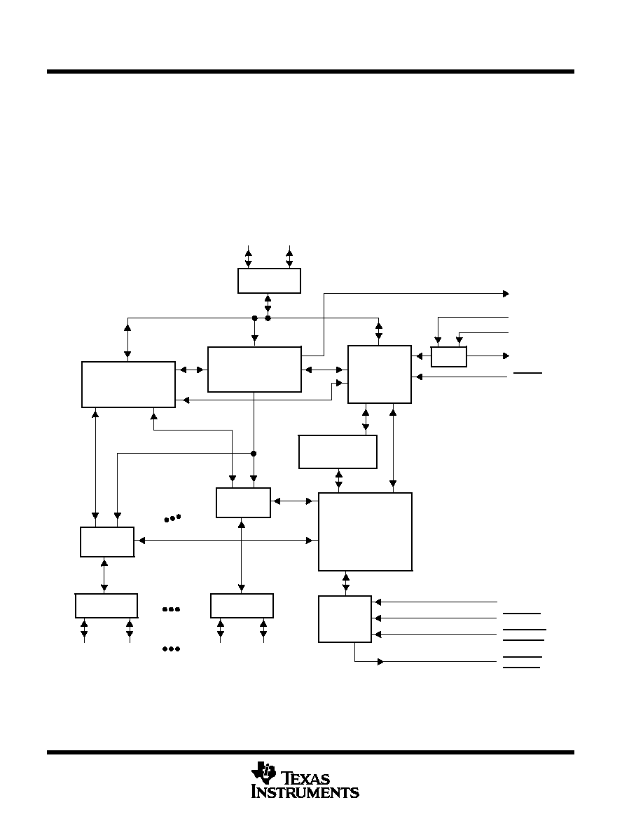
functional block diagram
Hub Repeater
Suspend / Resume
Logic and
Frame Timer
SIE
SIE Interface
Logic
Port 1
Logic
Hub / Device
Command
Decoder
Port 4
Logic
USB
Transceiver
Hub
Power
Logic
GANGED
BUSPWR
OVRCUR1 ≠
OVRCUR4
PWRON1 ≠
PWRON4
OSCOFF
XTAL1
21
23
18
10
9
OSC
DP0
DM0
4
5
USB
Transceiver
DP4
DM4
DP1
DM1
16
17
7
8
3, 1, 26, 19
2, 28, 25, 20
RESET
USB
Transceiver
22
XTAL2
(20)
SUSPND
(see Note B)
(32)
(35)
(34)
(11)
(10)
(48, 46, 38, 27)
(47, 44, 37, 29)
(1)
(2)
(23)
(24)
(6)
(7)
(25)
NOTES: A. Pins in parentheses are for TQFP package
B. SUSPND output only available in TQFP package

TUSB2040
4-PORT HUB FOR THE UNIVERSAL SERIAL BUS
SLLS260B ≠ NOVEMBER 1996 ≠ REVISED AUGUST 1997
3
POST OFFICE BOX 655303
∑
DALLAS, TEXAS 75265
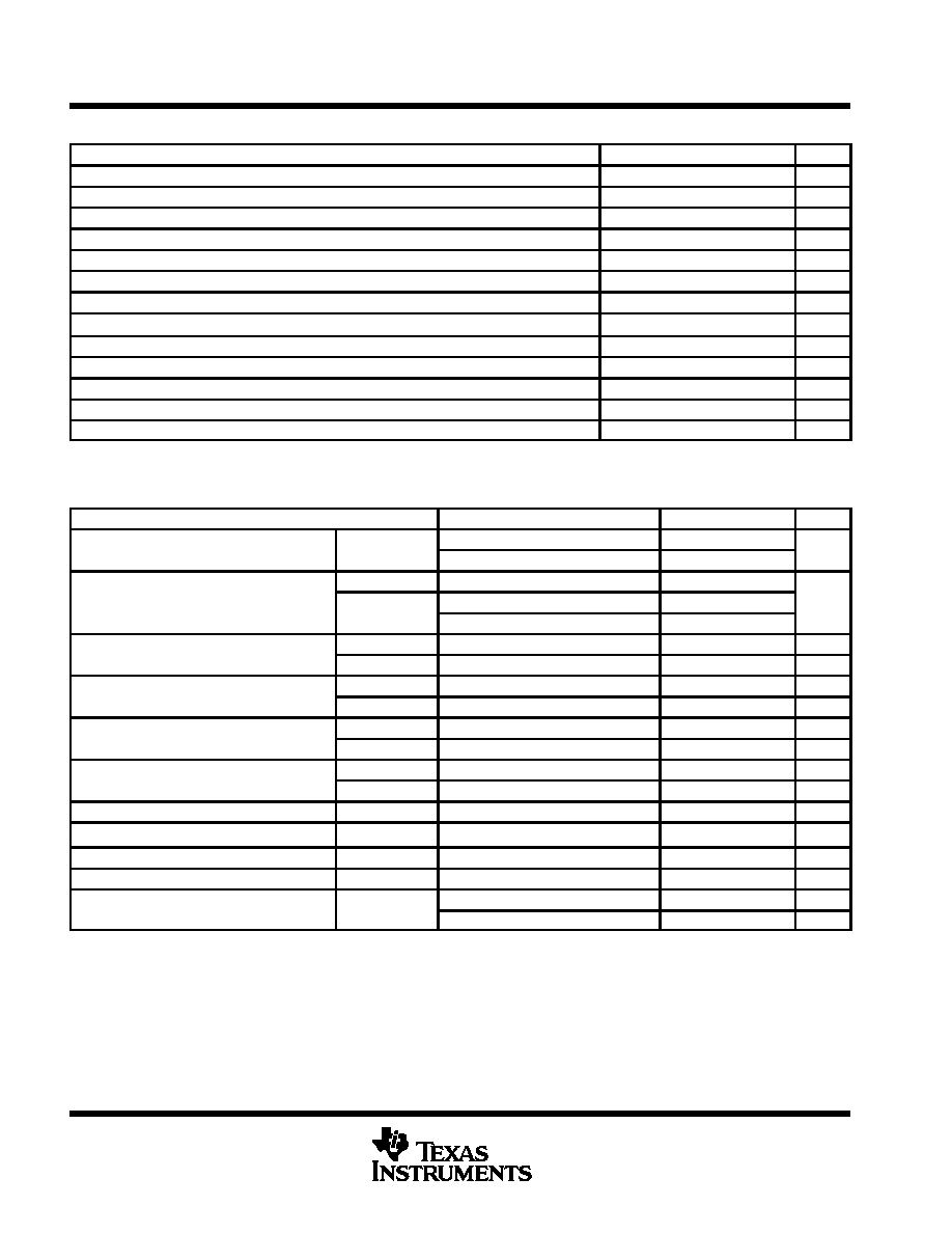
Terminal Functions
TERMINAL
I/O
DESCRIPTION
NAME
N NO.
PT NO.
I/O
DESCRIPTION
BUSPWR
9
10
I
Power source indicator. BUSPWR is an active low input that indicates whether the ports and the
hub derive power from the bus or are self-powered by the local supply. This standard TTL input
must not change dynamically during operation.
DM0
5
2
I/O
Root port USB differential data minus. DM0 paired with DP0 constitutes the upstream USB port.
DM1 ≠ DM4
8, 12,
15, 17
7, 14,
19, 24
I/O
USB differential data minus. DM1 ≠ DM4 paired with DP1 ≠ DP4 support up to four downstream
USB ports.
DP0
4
1
I/O
Root port USB differential data plus. DP0 paired with DM0 constitutes the upstream USB port.
DP1 ≠ DP4
7, 11,
14, 16
6, 13,
18, 23
I/O
USB differential data plus. DP1 ≠ DP4 paired with DM1 ≠ DM4 support up to four downstream
USB ports.
GANGED
10
11
I
Power switching/overcurrent detection mode. GANGED selects between gang or per port
switching and overcurrent detection for downstream ports. This standard TTL input must not
change dynamically during operation.
GND
6, 24
3, 36
Ground. GND terminals must be tied to ground for proper operation.
OSCOFF
21
32
I
Oscillator off. OSCOFF disables the internal oscillator for quiesent current draw (ICCQ) testing.
It must be tied low for proper operation.
OVRCUR1 ≠
OVRCUR4
3, 1,
26, 19
48, 46,
38, 27
I
Overcurrent indicators. OVRCUR1 ≠ OVRCUR4 are active low, standard TTL inputs. One
overcurrent indicator is available for each of the four downstream ports. In GANGED mode, one
implementation is to tie these inputs together. Alternatively, one OVRCUR input pin may be used
with the remaining OVRCUR pins tied to VCC.
PWRON1 ≠
PWRON4
2, 28,
25, 20
47, 44,
37, 29
O
Power-on/-off control signals. PWRON1 ≠ PWRON4 are active low, open-drain outputs. One
power on/off control switch is used for each of the four downstream ports. In GANGED mode, all
outputs are switched together.
RESET
18
25
I
Reset. RESET is an active low TTL input with hysteresis and must be asserted at power up. When
RESET is asserted it initializes all logic.
SUSPND
≠
20
O
Suspend status. SUSPND is an active high output that is available for external logic power down
operations. During the SUSPEND mode, SUSPND is high. SUSPND is low for normal operation.
VCC
13, 27
15, 41
3.3-V supply voltage
XTAL1
23
35
I
Crystal 1. XTAL1 is a 48-MHz crystal input with 50 % duty cycle. Operation at 48-MHz is four
times the USB full-speed bit rate of 12-Mbps.
XTAL2
22
34
O
Crystal 2. XTAL2 is a 48-MHz crystal output. Operation at 48-MHz is four times the USB full-speed
bit rate of 12-Mbps. This terminal is left open when using an oscillator.
absolute maximum ratings over operating free-air temperature range (unless otherwise noted)
Supply voltage range, V
CC
(see Note 1)
≠ 0.5 V to 3.8 V
. . . . . . . . . . . . . . . . . . . . . . . . . . . . . . . . . . . . . . . . . . . . .
Input voltgage range, V
I
≠ 0.5 V to V
CC
+ 0.5 V
. . . . . . . . . . . . . . . . . . . . . . . . . . . . . . . . . . . . . . . . . . . . . . . . . . . .
Output voltage range, V
O
≠0.5 V to V
CC
+ 0.5 V
. . . . . . . . . . . . . . . . . . . . . . . . . . . . . . . . . . . . . . . . . . . . . . . . . . . .
Input clamp current, I
IK
, (V
I
< 0 V or V
I
> V
CC
)
±
20 mA
. . . . . . . . . . . . . . . . . . . . . . . . . . . . . . . . . . . . . . . . . . . . .
Output clamp current, I
OK
, (V
O
< 0 V or V
O
> V
CC
)
±
20 mA
. . . . . . . . . . . . . . . . . . . . . . . . . . . . . . . . . . . . . . . . .
Storage temperature range, T
stg
≠ 65
∞
C to 150
∞
C
. . . . . . . . . . . . . . . . . . . . . . . . . . . . . . . . . . . . . . . . . . . . . . . . . . .
Stresses beyond those listed under "absolute maximum ratings" may cause permanent damage to the device. These are stress ratings only, and
functional operation of the device at these or any other conditions beyond those indicated under "recommended operating conditions" is not
implied. Exposure to absolute-maximum-rated conditions for extended periods may affect device reliability.
NOTE 1: All voltage levels are with respect to GND.
TUSB2040
4-PORT HUB FOR THE UNIVERSAL SERIAL BUS
SLLS260B ≠ NOVEMBER 1996 ≠ REVISED AUGUST 1997
4
POST OFFICE BOX 655303
∑
DALLAS, TEXAS 75265
recommended operating conditions
MIN
NOM
MAX
UNIT
Supply voltage, VCC
3
3.3
3.6
V
Input voltage, TTL/LVCMOS, VI
0
VCC
V
Output voltage, TTL/LVCMOS, VO
0
VCC
V
High-level input voltage, signal-ended receiver, VIH(REC)
2
VCC
V
Low-level input voltage, signal-ended receiver, VIL(REC)
0.8
V
High-level input voltage, TTL/LVCMOS, VIH(TTL)
2
VCC
V
Low-level input voltage, TTL/LVCMOS, VIL(TTL)
0.8
V
Operating free-air temperature, TA
0
70
∞
C
External series, differential driver resistor, R(DRV)
22 (≠5%)
22 (+5%)
Operating (dc differential driver) high speed mode, f(OPRH)
12
Mb/s
Operating (dc differential driver) low speed mode, f(OPRL)
1.5
Mb/s
Common mode, input range, differential receiver, V(ICR)
0.8
2.5
V
Input transition times, tt, TTL/LVCMOS
0
6
ns
electrical characteristics over recommended ranges of operating free-air temperature and supply
voltage (unless otherwise noted)
PARAMETER
TEST CONDITIONS
MIN
MAX
UNIT
VOH
High level output voltage
USB data lines
R(DRV) = 15 k
, to GND
2.8
3.6
V
VOH
High-level output voltage
USB data lines
IOH = ≠ 12 mA (without R(DRV))
VCC ≠ 0.5
V
TTL /LVCMOS
IOL = 4 mA
0.5
VOL
Low-level output voltage
USB data lines
R(DRV) = 1.5 k
to 3.6 V
0.3
V
USB data lines
IOL = 12 mA (without R(DRV))
0.5
VIT
Positive input threshold voltage
TTL /LVCMOS
2
V
VIT+
Positive input threshold voltage
Single-ended
0.8 V
VICR
2.5 V
1.8
V
VIT
Negative input threshold voltage
TTL /LVCMOS
0.8
V
VIT≠
Negative-input threshold voltage
Single-ended
0.8 V
VICR
2.5 V
1
V
Vh
Input hysteresis (V
V
)
TTL /LVCMOS
0.25
0.7
V
Vhys
Input hysteresis (VT+ ≠ VT≠)
Single-ended
0.8 V
VICR
2.5 V
300
500
mV
IOZ
High impedance output current
TTL/LVCMOS
V = VCC or GND
±
10
µ
A
IOZ
High-impedance output current
USB data lines
0 V
VO
VCC
±
10
µ
A
IIL
Low-level input current
TTL/LVCMOS
VI = GND
≠ 1
µ
A
IIH
High-level input current
TTL/LVCMOS
VI = VCC
1
µ
A
zo(DRV) Driver output impedance
USB data lines
Static VOH or VOL
7.1
19.9
VID
Differential input voltage
USB data lines
0.8 V
VICR
2.5 V
0.2
V
ICC
Input supply current
Normal operation
100
mA
ICC
Input supply current
Suspend mode
1
µ
A
Applies for input buffers with hysteresis
Applies for open drain buffers
TUSB2040
4-PORT HUB FOR THE UNIVERSAL SERIAL BUS
SLLS260B ≠ NOVEMBER 1996 ≠ REVISED AUGUST 1997
5
POST OFFICE BOX 655303
∑
DALLAS, TEXAS 75265
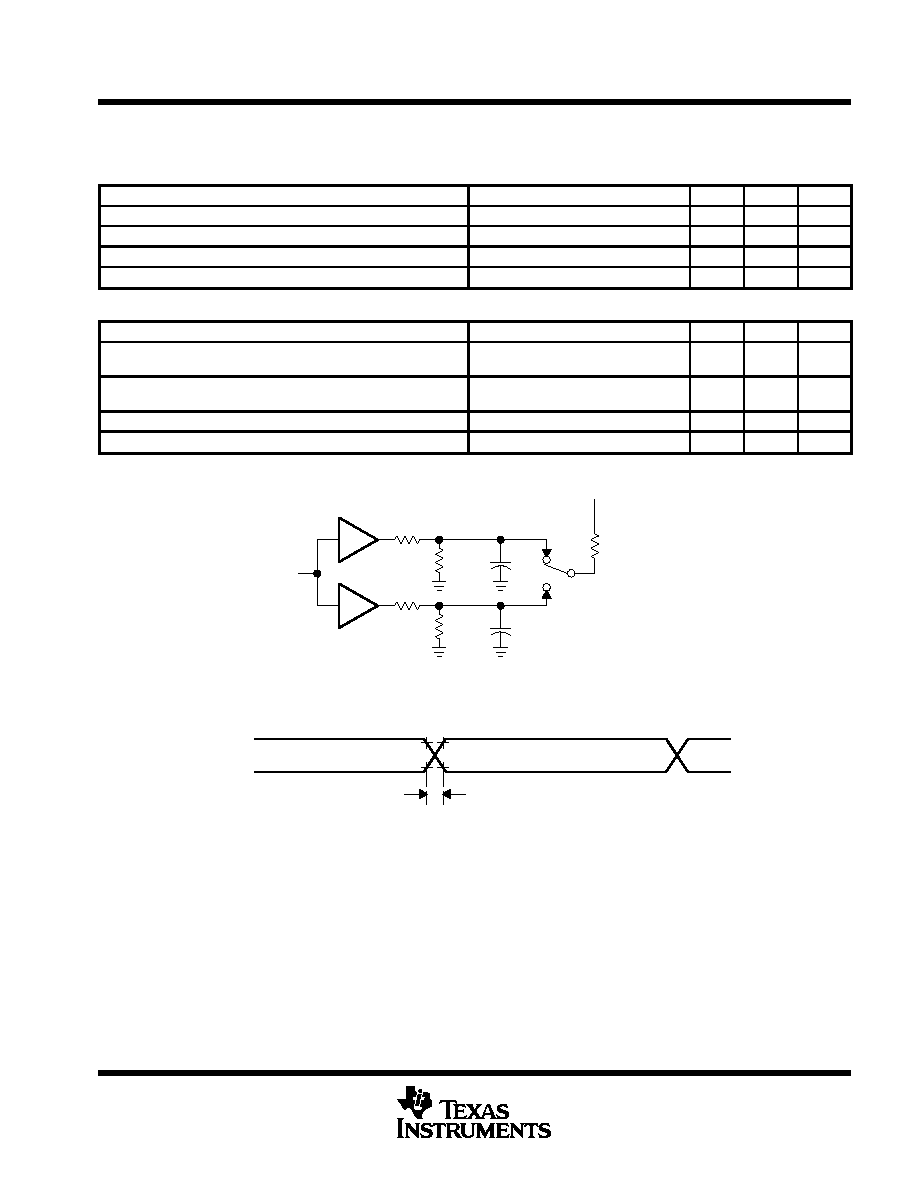
differential driver switching characteristics over recommended ranges of operating free-air
temperature and supply voltage, C
L
= 50 pF unless otherwise noted (see Figures 1 and 2)
full speed mode
PARAMETER
TEST CONDITIONS
MIN
MAX
UNIT
tr
Transition rise time for DP or DM
See Figure 1 and Figure 2
4
20
ns
tf
Transition fall time for DP or DM
See Figure 1 and Figure 2
4
20
ns
t(RFM)
Rise/fall time matching
(tr/tf) x 100
90
110
%
VO(CRS) Signal crossover output voltage
1.3
2.0
V
low speed mode
PARAMETER
TEST CONDITIONS
MIN
MAX
UNIT
tr
Transition rise time for DP to DM
CL = 50 pF to 350 pF, See Figure 1
and Figure 2
75
300
ns
tf
Transition fall time for DP to DM
CL = 50 pF to 350 pF, See Figure 1
and Figure 2
75
300
ns
t(RFM)
Rise/fall time matching
(tr/tf) x 100
80
120
%
VO(CRS) Signal crossover output voltage
CL = 50 pF to 350 pF
1.3
2.0
V
CL
15 k
15 k
CL
Full
Low
V(TERM) = 2.8 V
1.5 k
DP
DN
22
22
Figure 1. Differential Driver Switching Load
tr, tf
90%
10%
VO(CRS)
VOH
VOL
DM
DP
Figure 2. Differential Driver Timing Waveforms