 | –≠–ª–µ–∫—Ç—Ä–æ–Ω–Ω—ã–π –∫–æ–º–ø–æ–Ω–µ–Ω—Ç: U2825N | –°–∫–∞—á–∞—Ç—å:  PDF PDF  ZIP ZIP |
UC1825
UC2825
UC3825
SLUS235A - MARCH 1997 - REVISED MARCH 2004
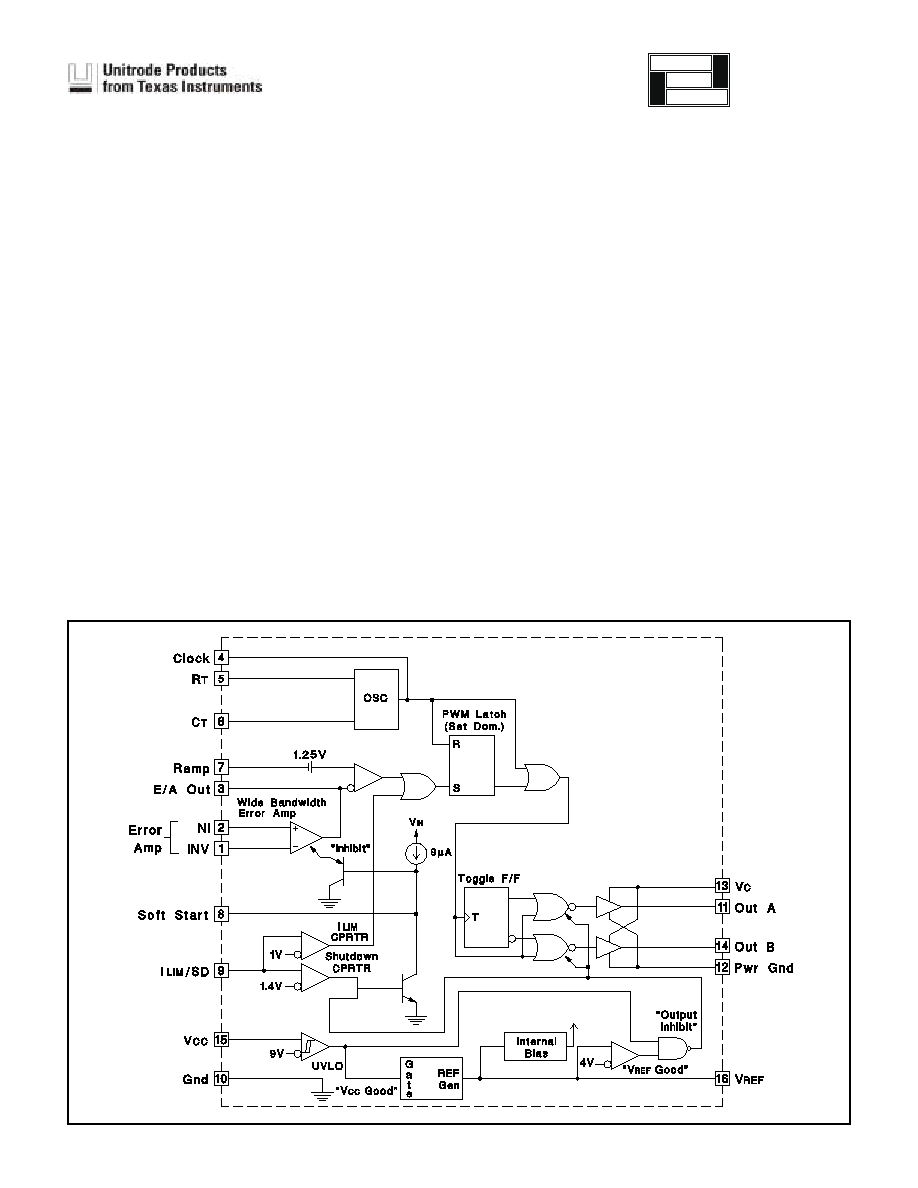
BLOCK DIAGRAM
∑
Compatible with Voltage or Current Mode
Topologies
∑
Practical Operation Switching Frequencies
to 1MHz
∑
50ns Propagation Delay to Output
∑
High Current Dual Totem Pole Outputs
(1.5A Peak)
∑
Wide Bandwidth Error Amplifier
∑
Fully Latched Logic with Double Pulse
Suppression
∑
Pulse-by-Pulse Current Limiting
∑
Soft Start / Max. Duty Cycle Control
∑
Under-Voltage Lockout with Hysteresis
∑
Low Start Up Current (1.1mA)
The UC1825 family of PWM control ICs is optimized for high fre-
quency switched mode power supply applications. Particular care
was given to minimizing propagation delays through the comparators
and logic circuitry while maximizing bandwidth and slew rate of the
error amplifier. This controller is designed for use in either cur-
rent-mode or voltage mode systems with the capability for input volt-
age feed-forward.
Protection circuitry includes a current limit comparator with a 1V
threshold, a TTL compatible shutdown port, and a soft start pin
which will double as a maximum duty cycle clamp. The logic is fully
latched to provide jitter free operation and prohibit multiple pulses at
an output. An under-voltage lockout section with 800mV of hysteresis
assures low start up current. During under-voltage lockout, the out-
puts are high impedance.
These devices feature totem pole outputs designed to source and
sink high peak currents from capacitive loads, such as the gate of a
power MOSFET. The on state is designed as a high level.
High Speed PWM Controller
FEATURES
DESCRIPTION
application
INFO
available
UDG-92030-2
2
UC1825
UC2825
UC3825
CONNECTION DIAGRAMS
DIL-16 (Top View)
J or N Package
SOIC-16 (Top View)
DW Package
PACKAGE PIN FUNCTION
FUNCTION
PIN
N/C
1
INV
2
NI
3
E/A Out
4
Clock
5
N/C
6
R
T
7
C
T
8
Ramp
9
Soft Start
10
N/C
11
ILIM/SD
12
Gnd
13
Out A
14
Pwr Gnd
15
N/C
16
V
C
17
Out B
18
V
CC
19
V
REF
5.1V
20
PLCC-20 & LCC-20
(Top View)
Q & L Packages
ABSOLUTE MAXIMUM RATINGS (Note 1)
Supply Voltage (Pins 13, 15) . . . . . . . . . . . . . . . . . . . . . . . . 30V
Output Current, Source or Sink (Pins 11, 14)
DC . . . . . . . . . . . . . . . . . . . . . . . . . . . . . . . . . . . . . . . . . . . 0.5A
Pulse (0.5
m
s) . . . . . . . . . . . . . . . . . . . . . . . . . . . . . . . . . . . 2.0A
Analog Inputs
(Pins 1, 2, 7). . . . . . . . . . . . . . . . . . . . . . . . . . . . . . . -0.3V to 7V
(Pin 8, 9) . . . . . . . . . . . . . . . . . . . . . . . . . . . . . . . . . -0.3V to 6V
Clock Output Current (Pin 4) . . . . . . . . . . . . . . . . . . . . . . . -5mA
Error Amplifier Output Current (Pin 3) . . . . . . . . . . . . . . . . 5mA
Soft Start Sink Current (Pin 8) . . . . . . . . . . . . . . . . . . . . . 20mA
Oscillator Charging Current (Pin 5) . . . . . . . . . . . . . . . . . . -5mA
Power Dissipation . . . . . . . . . . . . . . . . . . . . . . . . . . . . . . . . 1W
Storage Temperature Range . . . . . . . . . . . . . . -65∞C to +150∞C
Lead Temperature (Soldering, 10 seconds) . . . . . . . . . . 300∞C
Package
Q
JA
Q
JC
DIL-16J
80-120
28
(2)
DIL-16N
90
(1)
45
PLCC-20
43-75(1)
34
LCC-20
70-80
20
(2)
SOIC-16
50-120
(1)
35
THERMAL RATINGS TABLE
Q
Q
3
UC1825
UC2825
UC3825
ELECTRICAL CHARACTERISTICS:
Unless otherwise stated, these specifications apply for , R
T
= 3.65k, C
T
= 1nF, V
CC
= 15V, -55
∞
C<T
A
<125
∞
C for the UC1825, ≠40
∞
C<T
A
<85
∞
C for the UC2825, and 0
∞
C<T
A
<70
∞
C for the UC3825, T
A
=T
O.
UC1825
UC3825
PARAMETERS
TEST CONDITIONS
UC2825
MIN
TOP
MAX
MIN
TOP
MAX
UNITS
Reference Section
Output Voltage
T
O
= 25
∞
C, I
O
= 1mA
5.05
5.10
5.15
5.00
5.10
5.20
V
Line Regulation
10V < V
CC
< 30V
2
20
2
20
mV
Load Regulation
1mA < I
O
< 10mA
5
20
5
20
mV
Temperature Stability*
T
MIN
< T
A
< T
MAX
0.2
0.4
0.2
0.4
mV/
∞
C
Total Output Variation*
Line, Load, Temperature
5.00
5.20
4.95
5.25
V
Output Noise Voltage*
10Hz < f < 10kHz
50
50
µ
V
Long Term Stability*
T
J
= 125
∞
C, 1000hrs.
5
25
5
25
mV
Short Circuit Current
V
REF
= 0V
-15
-50
-100
-15
-50
-100
mA
Oscillator Section
Initial Accuracy*
T
J
= 2
∞
C
360
400
440
360
400
440
kHz
Voltage Stability*
10V < V
CC
< 30V
0.2
2
0.2
2
%
Temperature Stability*
T
MIN
< T
A
< T
MAX
5
5
%
Total Variation*
Line, Temperature
340
460
340
460
kHz
Oscillator Section (cont.)
Clock Out High
3.9
4.5
3.9
4.5
V
Clock Out Low
2.3
2.9
2.3
2.9
V
Ramp Peak*
2.6
2.8
3.0
2.6
2.8
3.0
V
Ramp Valley*
0.7
1.0
1.25
0.7
1.0
1.25
V
Ramp Valley to Peak*
1.6
1.8
2.0
1.6
1.8
2.0
V
Error Amplifier Section
Input Offset Voltage
10
15
mV
Input Bias Current
0.6
3
0.6
3
µ
A
Input Offset Current
0.1
1
0.1
1
µ
A
Open Loop Gain
1V < V
O
< 4V
60
95
60
95
dB
CMRR
1.5V < V
CM
< 5.5V
75
95
75
95
dB
PSRR
10V < V
CC
< 30V
85
110
85
110
dB
Output Sink Current
V
PIN 3
= 1V
1
2.5
1
2.5
mA
Output Source Current
V
PIN 3
= 4V
-0.5
-1.3
-0.5
-1.3
mA
Output High Voltage
I
PIN 3
= -0.5mA
4.0
4.7
5.0
4.0
4.7
5.0
V
Output Low Voltage
I
PIN 3
= 1mA
0
0 .5
1.0
0
0.5
1.0
V
Unity Gain Bandwidth*
3
5.5
3
5.5
MHz
Slew Rate*
6
12
6
12
V/
µ
s
4
UC1825
UC2825
UC3825
UC1825
UC3825
PARAMETERS
TEST CONDITIONS
UC2825
MIN
TOP
MAX
MIN
TOP
MAX
UNITS
PWM Comparator Section
Pin 7 Bias Current
V
PIN 7
= 0V
-1
-5
-1
-5
µ
A
Duty Cycle Range
0
80
0
85
%
Pin 3 Zero DC Threshold
V
PIN 7
= 0V
1.1
1.25
1.1
1.25
V
Delay to Output*
50
80
50
80
ns
Soft-Start Section
Charge Current
V
PIN 8
= 0.5V
3
9
20
3
9
20
µ
A
Discharge Current
V
PIN 8
= 1V
1
1
mA
Current Limit / Shutdown Section
Pin 9 Bias Current
0 < V
PIN 9
< 4V
15
10
µ
A
Current Limit Threshold
0.9
1.0
1.1
0.9
1.0
1.1
V
Shutdown Threshold
1.25
1.40
1.55
1.25
1.40
1.55
V
Delay to Output
50
80
50
80
ns
Output Section
Output Low Level
I
OUT
= 20mA
0.25
0.40
0.25
0.40
V
I
OUT
= 200mA
1.2
2.2
1.2
2.2
V
Output High Level
I
OUT
= -20mA
13.0
13.5
13.0
13.5
V
I
OUT
= -200mA
12.0
13.0
12.0
13.0
V
Collector Leakage
V
C
= 30V
100
500
10
500
µ
A
Rise/Fall Time*
CL = 1nF
30
60
30
60
ns
Under-Voltage Lockout Section
Start Threshold
8.8
9.2
9.6
8.8
9.2
9.6
V
UVLO Hysteresis
0.4
0.8
1.2
0.4
0.8
1.2
V
Supply Current Section
Start Up Current
V
CC
= 8V
1.1
2.5
1.1
2.5
mA
ICC
V
PIN 1
, V
PIN 7
, V
PIN 9
= 0V; V
PIN 2
= 1V
22
33
22
33
mA
ELECTRICAL CHARACTERISTICS:
Unless otherwise stated, these specifications apply for , R
T
= 3.65k, C
T
= 1nF, V
CC
= 15V, -55
∞
C<T
A
<125
∞
C for the UC1825, ≠40
∞
C<T
A
<85
∞
C for the UC2825, and 0
∞
C<T
A
<70
∞
C for the UC3825, T
A
=T
J.
5
UC1825
UC2825
UC3825
High speed circuits demand careful attention to layout
and component placement. To assure proper perfor-
mance of the UC1825 follow these rules: 1) Use a ground
plane. 2) Damp or clamp parasitic inductive kick energy
from the gate of driven MOSFETs. Do not allow the out-
put pins to ring below ground. A series gate resistor or a
shunt 1 Amp Schottky diode at the output pin will serve
this purpose. 3) Bypass V
CC
, V
C
, and V
REF
. Use 0.1
µ
F
monolithic ceramic capacitors with low equivalent series
inductance. Allow less than 1 cm of total lead length for
each capacitor between the bypassed pin and the ground
plane. 4) Treat the timing capacitor, CT, like a bypass ca-
pacitor.
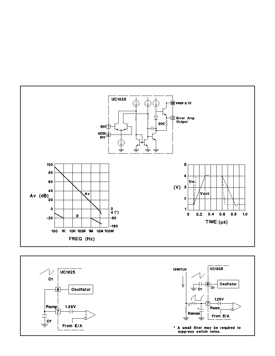
Open Loop Frequency Response
Unity Gain Slew Rate
Simplified Schematic
Error Amplifier Circuit
PWM Applications
Conventional (Voltage Mode)
Current-Mode
Printed Circuit Board Layout Considerations