 | –≠–ª–µ–∫—Ç—Ä–æ–Ω–Ω—ã–π –∫–æ–º–ø–æ–Ω–µ–Ω—Ç: UA2240CN | –°–∫–∞—á–∞—Ç—å:  PDF PDF  ZIP ZIP |
uA2240C
PROGRAMMABLE TIMER/COUNTER
SLFS045 ≠ JUNE 1978 ≠ REVISED MAY 1988
1
POST OFFICE BOX 655303
∑
DALLAS, TEXAS 75265
POST OFFICE BOX 1443
∑
HOUSTON, TEXAS 77251≠1443
D
Accurate Timing From Microseconds to
Days
D
Programmable Delays From 1 Time
Constant to 255 Time Constants
D
Outputs Compatible With TTL and CMOS
D
Wide Supply-Voltage Range
D
External Sync and Modulation Capability
description
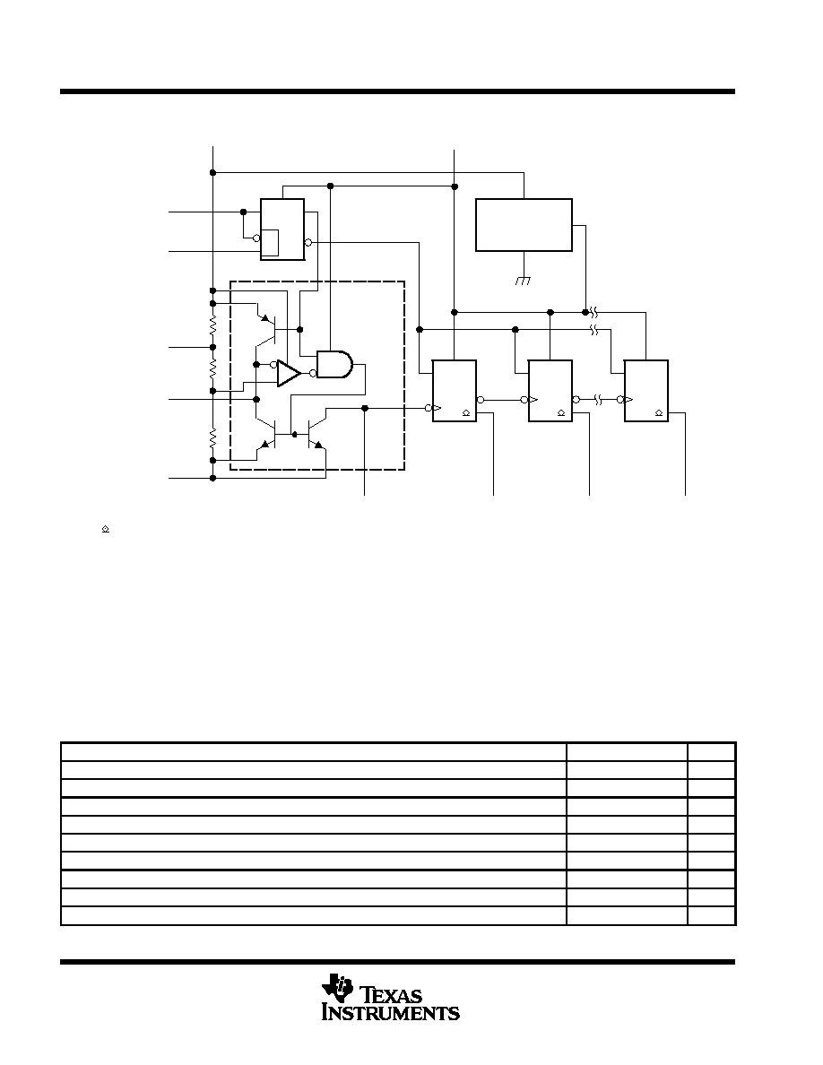
The uA2240C consists of a time-base oscillator,
an 8-bit counter, a control flip-flop, and a voltage
regulator. The frequency of the time-base oscillator is set by the time constant of an external resistor and
capacitor at R/C and can be synchronized or modulated by signals applied to the modulation input. The output
of the time-base section is applied directly to the input of the counter section and also appears at (TIME BASE).
TIME BASE may be used to monitor the frequency of the oscillator, to provide an output pulse to other circuitry,
or (with the time-base section disabled) to drive the counter input from an external source. The counter input
is activated on a negative-going transition. The reset input stops the time-base oscillator and sets each binary
output, Q0≠Q7, and the time-base output to a TTL high level. After resetting, the trigger input starts the oscillator
and all Q outputs go low. Once triggered, the uA2240C will ignore any signals at the trigger input until it is reset.
The uA2240C timer/counter may be operated in the free-running mode or with output-signal feedback to the
reset input for automatic reset. Two or more binary outputs may be connected together to generate complex
pulse patterns, or each output may be used separately to provide eight output frequencies. Using two circuits
in cascade can provide precise time delays of up to three years.
The uA2240C is characterized for operation from 0
∞
C to 70
∞
C.
AVAILABLE OPTIONS
SYMBOLIZATION
OPERATING
VT max
DEVICE
PACKAGE SUFFIX
TEMPERATURE RANGE
T
AT 25
∞
C
uA2240C
N
0
∞
C to 70
∞
C
2 V
Copyright
©
1988, Texas Instruments Incorporated
PRODUCTION DATA information is current as of publication date.
Products conform to specifications per the terms of Texas Instruments
standard warranty. Production processing does not necessarily include
testing of all parameters.
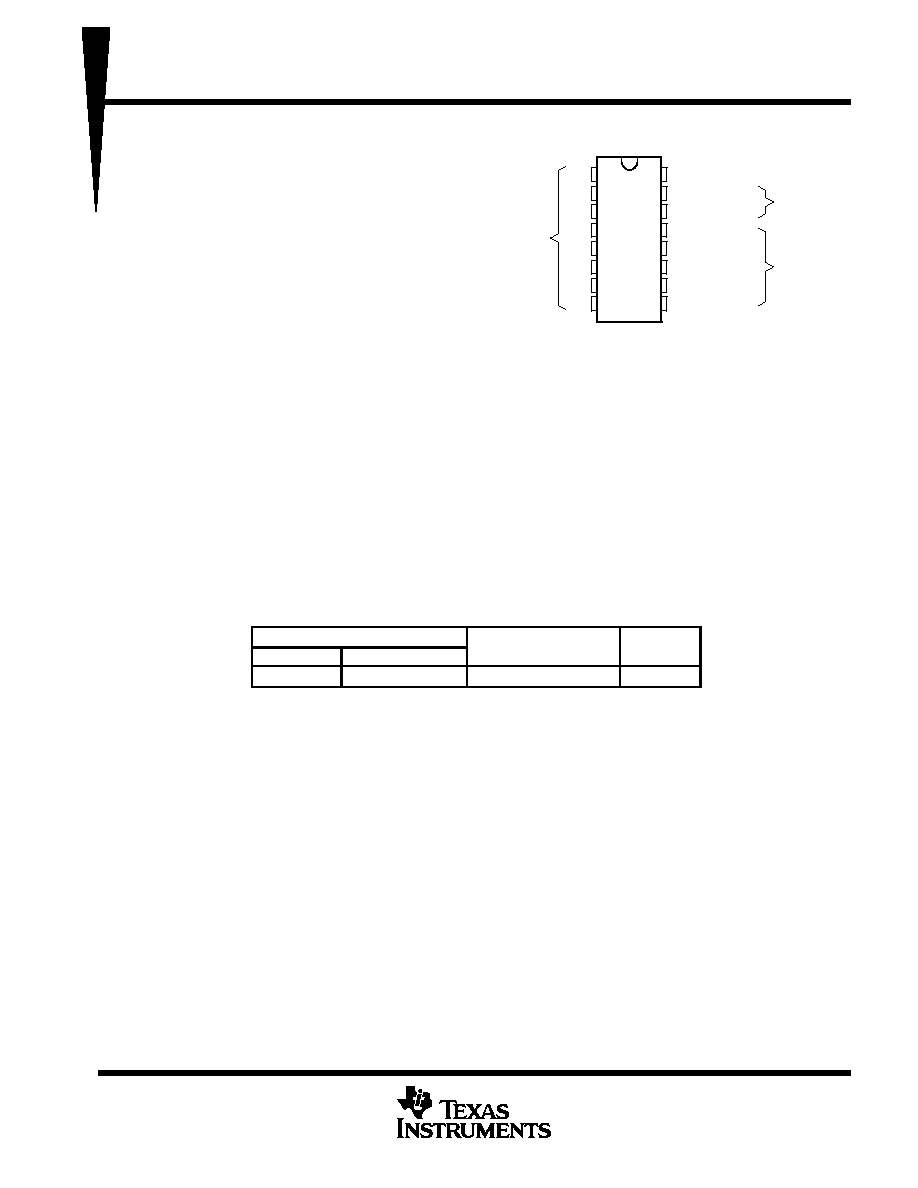
1
2
3
4
5
6
7
8
16
15
14
13
12
11
10
9
Q0
Q1
Q2
Q3
Q4
Q5
Q6
Q7
V
CC
REGULATOR
TIME BASE
R/C
MODULATION
TRIGGER
RESET
GND
N PACKAGE
(TOP VIEW)
OUTPUTS
OUTPUTS
INPUTS
uA2240C
PROGRAMMABLE TIMER/COUNTER
SLFS045 ≠ JUNE 1978 ≠ REVISED MAY 1988
2
POST OFFICE BOX 655303
∑
DALLAS, TEXAS 75265
POST OFFICE BOX 1443
∑
HOUSTON, TEXAS 77251≠1443
functional block diagram
T
VCC
Voltage
Regulator
S
& R
Time Base
Oscillator
S
S
S
T
T
TRIGGER
RESET
R/C
GND
= open-collector outputs
11
10
12
13
9
14
1
2
8
7 k
12 k
Time Base
Q0
Q1
Q7
16
15
REG OUT
MODULATION
absolute maximum ratings over operating free-air temperature range (unless otherwise noted)
Supply voltage, V
CC
(see Note 1)
18 V
. . . . . . . . . . . . . . . . . . . . . . . . . . . . . . . . . . . . . . . . . . . . . . . . . . . . . . . . . . .
Output voltage: Q0 ≠ Q7
18 V
. . . . . . . . . . . . . . . . . . . . . . . . . . . . . . . . . . . . . . . . . . . . . . . . . . . . . . . . . . . . . . . . . . . .
Output current: Q0 ≠ Q7
10 mA
. . . . . . . . . . . . . . . . . . . . . . . . . . . . . . . . . . . . . . . . . . . . . . . . . . . . . . . . . . . . . . . . . . .
Regulator output current
≠5 mA
. . . . . . . . . . . . . . . . . . . . . . . . . . . . . . . . . . . . . . . . . . . . . . . . . . . . . . . . . . . . . . . . . .
Continuous total dissipation at (or below) 25
∞
C free-air temperature
650 mW
. . . . . . . . . . . . . . . . . . . . . . . . . .
Operating free-air temperature range
0
∞
C to 70
∞
C
. . . . . . . . . . . . . . . . . . . . . . . . . . . . . . . . . . . . . . . . . . . . . . . . . .
Lead temperature 1,6 mm (1/16 inch) from case for 10 seconds
260
∞
C
. . . . . . . . . . . . . . . . . . . . . . . . . . . . . . .
NOTE 1: Voltage values are with respect to the network ground terminal.
recommended operating conditions
MIN
NOM
MAX
UNIT
Supply voltage, VCC (see Note 2)
4
14
V
Timing resistor
0.001
10
M
Timing capacitor
0.01
1000
µ
F
Counter input frequency (Pin 14)
1.5
MHz
Pull-up resistor, time-based output
20
k
Trigger and reset input pulse voltage
2
3
V
Trigger and reset input pulse duration
2
µ
s
External clock input pulse voltage
3
V
External clock input pulse duration
1
µ
s
NOTE 2: For operation with VCC
4.5 V, short regulator output to VCC.

uA2240C
PROGRAMMABLE TIMER/COUNTER
SLFS045 ≠ JUNE 1978 ≠ REVISED MAY 1988
3
POST OFFICE BOX 655303
∑
DALLAS, TEXAS 75265
POST OFFICE BOX 1443
∑
HOUSTON, TEXAS 77251≠1443
electrical characteristics at 25
∞
C free-air temperature
PARAMETER
TEST
CIRCUIT
TEST CONDITIONS
MIN
TYP
MAX
UNIT
Regulator output voltage
1
VCC = 5 V,
TRIGGER and RESET open or grounded
3.9
4.4
V
Regulator output voltage
2
VCC = 15 V,
TRIGGER and RESET open or grounded
5.8
6.3
6.8
V
Modulation input open circuit
1
VCC = 5 V,
TRIGGER and RESET open or grounded
2.8
3.5
4.2
V
voltage
1
VCC = 15 V,
TRIGGER and RESET open or grounded
10.5
V
Trigger threshold voltage
1
VCC = 5 V,
RESET at 0 V
1.4
2
V
High-level trigger current
1
VCC = 5 V,
TRIGGER at 2 V,
RESET at 0 V
10
µ
A
Reset threshold voltage
1
VCC = 5 V,
TRIGGER at 0 V
1.4
2
V
High-level reset current
1
VCC = 5 V,
TRIGGER at 0 V
10
µ
A
Counter input (time base)
threshold voltage
2
VCC = 5 V,
TRIGGER and RESET open or grounded
1
1.4
V
Low-level output current, Q0 ≠ Q7
2
VCC = 5 V,
VOL < 0.4 V
TRIGGER at 2 V,
RESET at 0 V,
2
4
mA
High-level output current, Q0 ≠ Q7
2
VOH = 15 V,
RESET at 2 V,
TRIGGER at 0 V
0.01
15
µ
A
1
VCC = 5 V,
TRIGGER at 0 V,
RESET at 5 V
4
7
Supply current
1
VCC = 15 V,
TRIGGER at 0 V,
RESET at 5 V
13
18
mA
3
V+ = 4 V
1.5
operating characteristics at 25
∞
C free-air temperature (unless otherwise noted)
PARAMETER
TEST
CIRCUIT
TEST CONDITIONS
MIN
TYP
MAX
UNIT
Initial error of time base
1
VCC = 5 V,
TRIGGER at 5 V,
RESET at 0 V
±
0.5
±
5
%
Temperature coefficient of time-
1
TA = 0
∞
C to 70
∞
C
VCC = 5 V
≠200
ppm/
∞
C
base period
1
TA = 0
∞
C to 70
∞
C
VCC = 15 V
≠80
ppm/
∞
C
Supply voltage sensitivity of time-
base period
1
VCC
8 V
≠0.08
≠0.3
%/ V
Time-base output frequency
1
VCC = 5 V,
R = MIN,
C = MIN
130
kHz
Propagation delay time
See Note 3
From TRIGGER input
1
µ
s
Propagation delay time
See Note 3
From RESET input
0.8
µ
s
Output rise time
2
RL = 3 k
CL = 10 pF
Q0 Q7
180
ns
Output fall time
2
RL = 3 k
,
CL = 10 pF
Q0 ≠ Q7
180
ns
For conditions shown as MIN or MAX, use the appropriate value specified under recommended operating conditions.
This is the time-base period error due only to the uA2240C and expressed as a percentage of nominal (1.00 RC).
NOTE 3: Propagation delay time is measured from the 50% point on the leading edge of an input pulse to the 50% point on the leading edge of
the resulting change of state at Q0.
uA2240C
PROGRAMMABLE TIMER/COUNTER
SLFS045 ≠ JUNE 1978 ≠ REVISED MAY 1988
4
POST OFFICE BOX 655303
∑
DALLAS, TEXAS 75265
POST OFFICE BOX 1443
∑
HOUSTON, TEXAS 77251≠1443
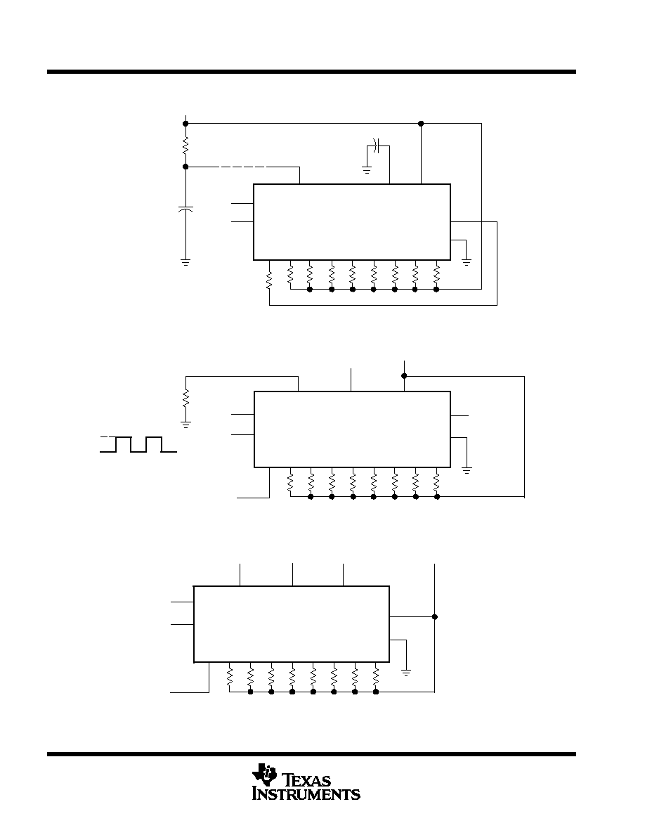
PARAMETER MEASUREMENT INFORMATION
TIME
BASE Q0
Q1
Q2
Q3
Q4
Q5
Q6
Q7
TRIG
RESET
Connected for
Operating Characteristics Tests Only
VCC
MOD
R/C
0.01
µ
F
VCC
R = 10 k
(Unless Otherwise
Specified)
C = 0.1
µ
F
(Unless Otherwise
Specified)
20 k
Each Q0 Thru Q7 Output Load = 10 k
uA2240C
REGULATOR
Figure 1. General Test Circuit
Time
Base Q0
Q1
Q2
Q3
Q4
Q5
Q6
Q7
TRIG
RESET
VCC
MOD
R/C
VCC
1 k
(Disables
Oscillator)
Each QO Thru Q7 Output Load = RL
(Open)
3 V
0 V
Input Signal for
Operating Characteristics
Tests Only
uA2240C
REGULATOR
Figure 2. Counter Test Circuit
TIME
BASE Q0
Q1
Q2
Q3
Q4
Q5
Q6
Q7
TRIG
RESET
VCC
MOD
R/C
(Open)
V+ = 4 V
Each QO Thru Q7 Output Load = 10 k
uA2240C
REGULATOR
These connections may be open or ungrounded for this test.
Figure 3. Reduced-Power Test Circuit (Time Base Disabled)

TRIGGER
RESET
TBO
Q0
Q1
Q7
Figure 5. Timing Diagram of Output Waveform
uA2240C
PROGRAMMABLE TIMER/COUNTER
SLFS045 ≠ JUNE 1978 ≠ REVISED MAY 1988
5
POST OFFICE BOX 655303
∑
DALLAS, TEXAS 75265
POST OFFICE BOX 1443
∑
HOUSTON, TEXAS 77251≠1443
TYPICAL CHARACTERISTICS
2.5
2
1.5
1
0.5
0
1
2
3
4
5
6
Modulation Voltage ≠ V
t
RC
≠ Normalize T
iming
NORMALIZED TIME-BASE PERIOD
vs
MODULATION INPUT VOLTAGE
Figure 4
APPLICATION INFORMATION
Figure 5 shows voltage waveforms for typical
operation of the uA2240C. If both RESET and
TRIGGER are low during power up, the timer/
counter will be in a reset state with all binary (Q)
outputs high and the oscillator stopped. In this state,
a high level on the trigger input starts the time-base
oscillator. The initial negative-going pulse from the
oscillator sets the Q outputs to low logic levels at the
beginning of the first time-base period. The uA2240C
will ignore any further signals at the TRIGGER until
after a reset signal is applied to RESET. With
TRIGGER low, a high level at the reset input will set
Q outputs high and stop the time-base oscillator. If
the reset signal occurs while TRIGGER is high, the
reset is ignored. If RESET remains high when
TRIGGER goes low, the uA2240C will reset.