 | –≠–ª–µ–∫—Ç—Ä–æ–Ω–Ω—ã–π –∫–æ–º–ø–æ–Ω–µ–Ω—Ç: UA733C | –°–∫–∞—á–∞—Ç—å:  PDF PDF  ZIP ZIP |

The
and no longer supplied.
m
A733M is obsolete
mA733C, mA733M
DIFFERENTIAL VIDEO AMPLIFIERS
SLFS027B - NOVEMBER 1970 - REVISED MAY 2004
1
POST OFFICE BOX 655303
∑
DALLAS, TEXAS 75265
D
200-MHz Bandwidth
D
250-k
Input Resistance
D
Selectable Nominal Amplification of 10,
100, or 400
D
No Frequency Compensation Required
1
2
3
4
5
10
9
8
7
6
IN+
GAIN ADJ 2A
GAIN ADJ 1A
V
CC -
OUT+
IN -
GAIN ADJ 2B
GAIN ADJ 1B
V
CC+
OUT-
m
A733M . . . U PACKAGE
(TOP VIEW)
NC
No internal connection
1
2
3
4
5
6
7
14
13
12
11
10
9
8
IN+
NC
GAIN ADJ 2A
GAIN ADJ 1A
V
CC-
NC
OUT+
IN-
NC
GAIN ADJ 2B
GAIN ADJ 1B
V
CC+
NC
OUT-
m
A733C . . . D, N, OR NS PACKAGE
m
A733M . . . J PACKAGE
(TOP VIEW)
description/ordering information
The
µ
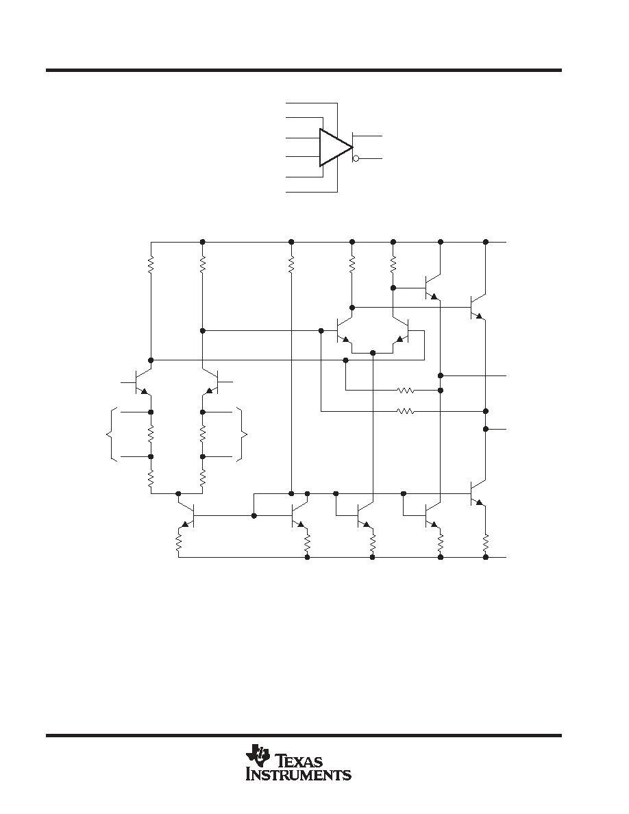
A733 is a monolithic two-stage video amplifier with differential inputs and differential outputs. Internal
series-shunt feedback provides wide bandwidth, low phase distortion, and excellent gain stability.
Emitter-follower outputs enable the device to drive capacitive loads, and all stages are current-source biased
to obtain high common-mode and supply-voltage rejection ratios.
Fixed differential amplification of 10 V/ V, 100 V/ V, or 400 V/ V may be selected without external components,
or amplification may be adjusted from 10 V/ V to 400 V/ V by the use of a single external resistor connected
between 1A and 1B. No external frequency-compensating components are required for any gain option.
The device is particularly useful in magnetic-tape or disc-file systems using phase or NRZ encoding and in
high-speed thin-film or plated-wire memories. Other applications include general-purpose video and pulse
amplifiers where wide bandwidth, low phase shift, and excellent gain stability are required.
The
µ
A733C is characterized for operation from 0
∞
C to 70
∞
C; the
µ
A733M is characterized for operation over
the full military temperature range of -55
∞
C to 125
∞
C.
ORDERING INFORMATION
TA
PACKAGE
ORDERABLE
PART NUMBER
TOP-SIDE
MARKING
P-DIP (N)
Tube of 25
UA733CN
UA733CN
0
∞
C to 70
∞
C
SOIC (D)
Tube of 50
UA733CD
UA733C
0
∞
C to 70
∞
C
SOIC (D)
Reel of 2500
UA733CDR
UA733C
SOP (NS)
Reel of 2000
UA733CNSR
UA733
Package drawings, standard packing quantities, thermal data, symbolization, and PCB design guidelines
are available at www.ti.com/sc/package.
Copyright
2004, Texas Instruments Incorporated
PRODUCTION DATA information is current as of publication date.
Products conform to specifications per the terms of Texas Instruments
standard warranty. Production processing does not necessarily include
testing of all parameters.
Please be aware that an important notice concerning availability, standard warranty, and use in critical applications of
Texas Instruments semiconductor products and disclaimers thereto appears at the end of this data sheet.
The
and no longer supplied.
m
A733M is obsolete
mA733C, mA733M
DIFFERENTIAL VIDEO AMPLIFIERS
SLFS027B - NOVEMBER 1970 - REVISED MAY 2004
2
POST OFFICE BOX 655303
∑
DALLAS, TEXAS 75265
symbol
+
_
GAIN ADJ 1A
GAIN ADJ 2A
IN +
IN -
GAIN ADJ 1B
GAIN ADJ 2B
OUT+
OUT-
schematic
1A
2A
GAIN
ADJ
IN +
IN -
1B
2B
GAIN
ADJ
590
590
300
2.4 k
2.4 k
10 k
1.1 k
1.1 k
50
50
1.4 k
300
400
400
VCC+
OUT+
OUT -
VCC -
7 k
7 k
Component values shown are nominal.
The
and no longer supplied.
m
A733M is obsolete
mA733C, mA733M
DIFFERENTIAL VIDEO AMPLIFIERS
SLFS027B - NOVEMBER 1970 - REVISED MAY 2004
3
POST OFFICE BOX 655303
∑
DALLAS, TEXAS 75265
absolute maximum ratings over operating free-air temperature range (unless otherwise noted)
m
A733C
m
A733M
UNIT
Supply voltage VCC+ (see Note 1)
8
8
V
Supply voltage VCC- (see Note 1)
- 8
- 8
V
Differential input voltage
±
5
±
5
V
Common-mode input voltage
±
6
±
6
V
Output current
10
10
mA
Continuous total power dissipation
See Dissipation Rating Table
D package
86
Package thermal impedance,
q
JA (see Notes 2 and 3)
N package
80
∞
C/W
Package thermal impedance,
q
JA (see Notes 2 and 3)
NS package
76
C/W
Maximum junction temperature, TJ
150
∞
C
Lead temperature 1,6 mm (1/16 inch) from case for 60 seconds
J or U package
300
∞
C
Storage temperature range, Tstg
- 65 to 150
- 65 to 150
∞
C
Stresses beyond those listed under absolute maximum ratings may cause permanent damage to the device. This is a stress rating only, and
functional operation of the device at these or any other conditions beyond those indicated in the recommended operating conditions section of
this specification is not implied. Exposure to absolute-maximum-rated conditions for extended periods may affect device reliability.
NOTES:
1. All voltage values, except differential input voltages, are with respect to the midpoint between VCC+ and VCC≠.
2. Maximum power dissipation is a function of TJ(max),
q
JA, and TA. The maximum allowable power dissipation at any allowable
ambient temperature is PD = (TJ(max) ≠ TA)/
q
JA. Operating at the absolute maximum TJ of 150
∞
C can affect reliability.
3. The package thermal impedance is calculated in accordance with JESD 51-7.
DISSIPATION RATING TABLE
PACKAGE
TA
25
∞
C
POWER RATING
DERATING
FACTOR
DERATE
ABOVE TA
TA = 70
∞
C
POWER RATING
TA = 125
∞
C
POWER RATING
J (
µ
A733M)
500 mW
11.0 mW/
∞
C
104
∞
C
500 mW
269 mW
The
and no longer supplied.
m
A733M is obsolete
mA733C, mA733M
DIFFERENTIAL VIDEO AMPLIFIERS
SLFS027B - NOVEMBER 1970 - REVISED MAY 2004
4
POST OFFICE BOX 655303
∑
DALLAS, TEXAS 75265
electrical characteristics, V
CC
±
=
±
6 V, T
A
= 25
∞
C
PARAMETER
FIGURE
TEST CONDITIONS
GAIN
m
A733C
m
A733M
UNIT
PARAMETER
FIGURE
TEST CONDITIONS
GAIN
OPTION
MIN
TYP
MAX
MIN
TYP
MAX
UNIT
Large-signal
differential
1
250
400
600
300
400
500
AVD
Large-signal
differential
voltage
1
VOD = 1 V
2
80
100
120
90
100
110
V/ V
AVD
voltage
amplification
1
VOD = 1 V
3
8
10
12
9
10
11
V/ V
1
50
50
BW
Bandwidth
2
RS = 50
2
90
90
MHz
BW
Bandwidth
2
RS = 50
3
200
200
MHz
IIO
Input offset
current
Any
0.4
5
0.4
3
µ
A
IIB
Input bias current
Any
9
30
9
20
µ
A
VICR
Common-mode
input voltage
range
1
Any
±
1
±
1
V
VOC
Common-mode
output voltage
1
Any
2.4
2.9
3.4
2.4
2.9
3.4
V
VOO
Output offset
1
1
0.6
1.5
0.6
1.5
V
VOO
Output offset
voltage
1
2 & 3
0.35
1.5
0.35
1
V
VOPP
Maximum peak-
to-peak output
voltage swing
1
Any
3
4.7
3
4.7
V
1
4
4
ri
Input resistance
3
VOD
1 V
2
10
24
20
24
k
ri
Input resistance
3
VOD
1 V
3
250
250
k
ro
Output resistance
20
20
Ci
Input capacitance
3
VOD
1 V
2
2
2
pF
CMRR
Common-mode
4
VIC =
±
1 V,
f
100 kHz
2
60
86
60
86
dB
CMRR
Common-mode
rejection ration
4
VIC =
±
1 V,
f = 5 MHz
2
70
70
dB
kSVR
Supply voltage
rejection ratio
(
VCC/(
VIO)
1
VCC
±
=
±
0.5 V
2
50
70
50
70
dB
Vn
Broadband
equivalent input
noise voltage
5
BW = 1 kHz to 10 MHz
Any
12
12
µ
V
Propagation
RS = 50
,
1
7.5
7.5
tpd
Propagation
delay time
2
RS = 50
,
Output voltage
step = 1 V
2
6.0
10
6.0
10
ns
tpd
delay time
2
Output voltage
step = 1 V
3
3.6
3.6
ns
RS = 50
,
1
10.5
10.5
tr
Rise time
2
RS = 50
,
Output voltage
step = 1 V
2
4.5
12
4.5
10
ns
tr
Rise time
2
Output voltage
step = 1 V
3
2.5
2.5
ns
Isink(max)
Maximum output
sink current
Any
2.5
3.6
2.5
3.6
mA
ICC
Supply current
No load,
No signal
Any
16
24
16
24
mA
The gain option is selected as follows:
Gain Option 1: Gain-adjust pin 1A is connected to pin 1B, and pins 2A and 2B are open.
Gain Option 2: Gain-adjust pin 1A and pin 1B are open, pin 2A is connected to pin 2B.
Gain Option 3: All four gain-adjust pins are open.

The
and no longer supplied.
m
A733M is obsolete
mA733C, mA733M
DIFFERENTIAL VIDEO AMPLIFIERS
SLFS027B - NOVEMBER 1970 - REVISED MAY 2004
5
POST OFFICE BOX 655303
∑
DALLAS, TEXAS 75265
electrical characteristics, V
CC
±
=
±
6 V, T
A
= 0
∞
C to 70
∞
C f
or
m
A733C, - 55
∞
C to 125
∞
C for
m
A733M
PARAMETER
FIGURE
TEST CONDITIONS
GAIN
m
A733C
m
A733M
UNIT
PARAMETER
FIGURE
TEST CONDITIONS
GAIN
OPTION
MIN
MAX
MIN
MAX
UNIT
Large-signal differential
1
250
600
200
600
AVD
Large-signal differential
voltage amplification
1
VOD = 1 V
2
80
120
80
120
V/ V
AVD
voltage amplification
1
VOD = 1 V
3
8
12
8
12
V/ V
IIO
Input offset current
Any
6
5
µ
A
IIB
Input bias current
Any
40
40
µ
A
VICR
Common-mode input
voltage range
1
Any
±
1
±
1
V
VOO
Output offset voltage
1
1
1.5
1.5
V
VOO
Output offset voltage
1
2 & 3
1.5
1.2
V
VOPP
Maximum peak-to-peak
output voltage swing
1
Any
2.8
2.5
V
ri
Input resistance
3
VOD
1 V
2
8
8
k
CMRR
Common-mode rejection
ratio
4
VIC = +1 V,
f
100 kHz
2
50
50
dB
kSVR
Supply voltage rejection
ratio (
VCC /(
VIO)
1
VCC
±
=
±
0.5 V
2
50
50
dB
Isink(max)
Maximum output sink
current
Any
2.5
2.2
mA
ICC
Supply current
No load,
No signal
Any
27
27
mA
The gain option is selected as follows:
Gain Option 1: Gain-adjust pin 1A is connected to pin 1B, and pins 2A and 2B are open.
Gain Option 2: Gain-adjust pin 1A and pin 1B are open, pin 2A is connected to pin 2B.
Gain Option 3: All four gain-adjust pins are open.