 | –≠–ª–µ–∫—Ç—Ä–æ–Ω–Ω—ã–π –∫–æ–º–ø–æ–Ω–µ–Ω—Ç: uA747-1M | –°–∫–∞—á–∞—Ç—å:  PDF PDF  ZIP ZIP |
uA747C, uA747M
DUAL GENERAL-PURPOSE OPERATIONAL AMPLIFIERS
SLOS009A ≠ D971, FEBRUARY 1971 ≠ REVISED OCTOBER 1990
POST OFFICE BOX 655303
∑
DALLAS, TEXAS 75265
Copyright
©
1990, Texas Instruments Incorporated
1
∑
No Frequency Compensation Required
∑
Low Power Consumption
∑
Short-Circuit Protection
∑
Offset-Voltage Null Capability
∑
Wide Common-Mode and Differential
Voltage Ranges
∑
No Latch-Up
∑
Designed to Be Interchangeable With
Fairchild
µ
A747C and
µ
A747M
description
The uA747 is a dual general-purpose operational
amplifier featuring offset-voltage null capability.
Each half is electrically similar to uA741.
The high common-mode input voltage range and
the absence of latch-up make this amplifier ideal
for voltage-follower applications. The device is
short-circuit protected and the internal frequency
compensation ensures stability without external
components. A low-value potentiometer may be
connected between the offset null inputs to null out
the offset voltage as shown in Figure 2.
The uA747C is characterized for operation from
0
∞
C to 70
∞
C; the uA747M is characterized for
operation over the full military temperature range
of ≠ 55
∞
C to 125
∞
C.
symbol (each amplifier)
IN+
IN ≠
OUT
OFFSET N1
OFFSET N2
œœœ
œœœ
œœœ
œœœ
≠
+
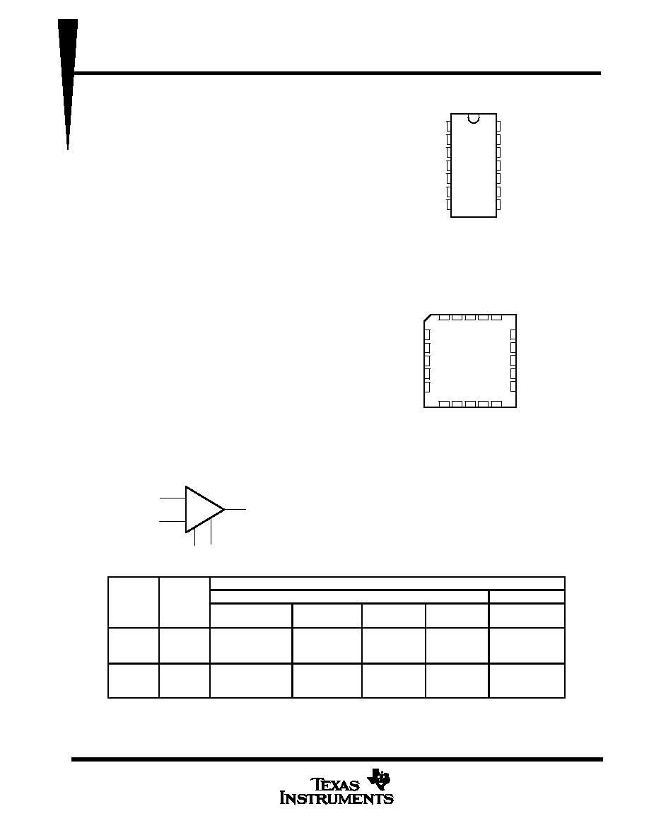
AVAILABLE OPTIONS
PACKAGE
VIO Max
14-PIN
20-PIN
TA
VIO Max
AT 25
∞
C
SMALL OUTLINE
(D)
CERAMIC DIP
(J)
PLASTIC DIP
(N)
FLAT PACK
(W)
CHIP CARRIER
(FK)
0
∞
C
to
70
∞
C
6 mV
uA747CD
--
uA747CN
--
--
≠55
∞
C
to
125
∞
C
5 mV
--
uA747MJ
--
uA747MW
uA747MFK
The D package is available taped and reeled. Add the suffix R to the device type, (i.e., uA747CDR).
1
2
3
4
5
6
7
14
13
12
11
10
9
8
IN ≠
IN +
OFFSET 1N2
V
CC ≠
OFFSET 2N2
IN +
IN ≠
OFFSET 1N1
1 V
CC +
OUT
NC
OUT
2 V
CC +
OFFSET 2N1
D, J, N, OR W PACKAGE
(TOP VIEW)
3
2
1 20 19
9 10 11 12 13
4
5
6
7
8
18
17
16
15
14
OUT
NC
NC
NC
OUT
OFFSET 1N2
NC
V
CC ≠
NC
OFFSET 2N2
uA747m . . . FK PACKAGE
(TOP VIEW)
IN
+
IN
≠
NC
OFFSET
1N1
IN
+
IN
≠
NC
NC ≠ No internal connection
OFFSET
2N1
CC
+
1 V
CC
+
2 V
The two positive supply terminals (1 VCC + and 2 VCC +) are
connected together internally.
PRODUCTION DATA information is current as of publication date.
Products conform to specifications per the terms of Texas Instruments
standard warranty. Production processing does not necessarily include
testing of all parameters.
uA747C, uA747M
DUAL GENERAL-PURPOSE OPERATIONAL AMPLIFIERS
SLOS009A ≠ D971, FEBRUARY 1971 ≠ REVISED OCTOBER 1990
POST OFFICE BOX 655303
∑
DALLAS, TEXAS 75265
2
schematic (each amplifier)
VCC +
OUT
VCC ≠
IN ≠
IN +
OFFSET N2
OFFSET N1
absolute maximum ratings over operating free-air temperature range (unless otherwise noted)
uA747C
uA747M
UNIT
Supply voltage, VCC + (see Note 1)
18
22
V
Supply voltage, VCC ≠ (see Note 1)
≠ 18
≠ 22
V
Differential input voltage (see Note 2)
±
30
±
30
V
Input voltage any input (see Notes 1 and 3)
±
15
±
15
V
Voltage between any offset null terminal (N1/N2) and VCC ≠
±
0.5
±
0.5
V
Duration of output short circuit (see Note 4)
unlimited
unlimited
Continuous total dissipation
See Dissipation Rating Table
Operating free-air temperature range
0 to 70
≠ 55 to 125
∞
C
Storage temperature range
≠ 65 to 150
≠ 65 to 150
∞
C
Case temperature for 60 seconds
FK package
260
∞
C
Lead temperature 1,6 mm (1/16 inch) from case for 60 seconds
J or W package
300
∞
C
Lead temperature 1,6 mm (1/16 inch) from case for 10 seconds
D or N package
260
∞
C
NOTES: 1. All voltage values, unless otherwise noted, are with respect to the midpoint between VCC + and VCC ≠.
2. Differential voltages are at the noninverting input terminal with respect to the inverting input terminal.
3. The magnitude of the input voltage must never exceed the magnitude of the supply voltage or 15 V, whichever is less.
4. The output may be shorted to ground or either power supply. For the uA747M only, the unlimited duration of the short circuit applies
at (or below) 125
∞
C case temperature or 75
∞
C free-air temperature.
DISSIPATION RATING TABLE
PACKAGE
TA
25
∞
C
POWER RATING
DERATING
FACTOR
DERATE
ABOVE TA
TA = 70
∞
C
POWER RATING
TA = 125
∞
C
POWER RATING
D
800 mW
7.6 mW/
∞
C
45
∞
C
608 mW
--
FK
800 mW
11.0 mW/
∞
C
77
∞
C
800 mW
275 mW
J
800 mW
11.0 mW/
∞
C
77
∞
C
800 mW
275 mW
N
800 mW
9.2 mW/
∞
C
63
∞
C
736 mW
--
W
800 mW
8.0 mW/
∞
C
50
∞
C
640 mW
200 mW

uA747C, uA747M
DUAL GENERAL-PURPOSE OPERATIONAL AMPLIFIERS
SLOS009A ≠ D971, FEBRUARY 1971 ≠ REVISED OCTOBER 1990
POST OFFICE BOX 655303
∑
DALLAS, TEXAS 75265
3
electrical characteristics at specified free-air temperature, V
CC
±
=
±
15 V
PARAMETER
TEST CONDITIONS
TA
uA747C
uA747M
UNIT
PARAMETER
TEST CONDITIONS
TA
MIN
TYP
MAX
MIN
TYP
MAX
UNIT
VIO
Input offset voltage
VO = 0
25
∞
C
1
6
1
5
mV
VIO
Input offset voltage
VO = 0
Full range
7.5
6
mV
VIO(adj)
Offset voltage
adjust range
25
∞
C
±
15
±
15
mV
IIO
Input offset current
25
∞
C
20
200
20
200
nA
IIO
Input offset current
Full range
300
500
nA
IIB
Input bias current
25
∞
C
80
500
80
500
nA
IIB
Input bias current
Full range
800
1500
nA
VICR
Common-mode
25
∞
C
±
12
±
13
±
12
±
13
V
VICR
input voltage range
Full range
±
12
±
12
V
RL= 10 k
25
∞
C
24
28
24
28
VO(PP)
Maximum peak-to-peak
RL
10 k
Full range
24
24
V
VO(PP)
output voltage swing
RL= 2 k
25
∞
C
20
26
20
26
V
RL
2 k
Full range
20
20
AVD
Large-signal differential
RL
2 k
,
25
∞
C
25
200
50
200
V/mV
AVD
voltage amplification
VO =
±
10 V
Full range
15
25
V/mV
ri
Input resistance
25
∞
C
0.3
2
0.3*
2
M
ro
Output resistance
See Note 5
25
∞
C
75
75
Ci
Input capacitance
25
∞
C
1.4
1.4
pF
CMRR
Common-mode
VIC = VICR
25
∞
C
70
90
70
90
dB
CMRR
rejection ratio
VIC = VICR
Full range
70
70
dB
kSVS
Supply-voltage
sensitivity
VCC =
±
9 V to
±
15 V
25
∞
C
30
150
30
150
µ
V/V
kSVS
sensitivity
(
VIO /
VCC)
VCC =
±
9 V to
±
15 V
Full range
150
150
µ
V/V
IOS
Short-circuit
output current
25
∞
C
±
25
±
40
±
25
±
40
mA
ICC
Supply current
No load
25
∞
C
1.7
2.8
1.7
2.8
mA
ICC
y
(each amplifier)
No load
Full range
3.3
3.3
mA
PD
Power dissipation
No load
VO = 0
25
∞
C
50
85
50
85
mW
PD
(each amplifier)
No load, VO = 0
Full range
100
100
mW
Vo1/Vo2
Channel separation
25
∞
C
120
120
0
dB
All characteristics are measured under open-loop conditions with zero common-mode input voltage unless otherwise specified.
Full range for uA747C is 0
∞
C to 70
∞
C and for uA747M is ≠ 55
∞
C to 125
∞
C.
*On products compliant to MIL-STD-883, Class B, this parameter is not production tested.
NOTE 5: This typical value applies only at frequencies above a few hundred hertz because of the effects of drift and thermal feedback.
operating characteristics, V
CC
±
=
±
15 V, T
A
= 25
∞
C
PARAMETER
TEST CONDITIONS
MIN
TYP
MAX
UNIT
tr
Rise time
VI = 20 mV RL = 2 k
CL = 100 pF See Figure 1
0.3
µ
s
Overshoot factor
VI = 20 mV, RL = 2 k
, CL = 100 pF, See Figure 1
5%
SR
Slew rate at unity gain
VI = 10 mV, RL = 2 k
, CL = 100 pF, See Figure 1
0.5
V/
µ
s
uA747C, uA747M
DUAL GENERAL-PURPOSE OPERATIONAL AMPLIFIERS
SLOS009A ≠ D971, FEBRUARY 1971 ≠ REVISED OCTOBER 1990
POST OFFICE BOX 655303
∑
DALLAS, TEXAS 75265
4
PARAMETER MEASUREMENT INFORMATION
≠
+
VI
0 V
Input
OUT
RL = 2 k
CL = 100 pF
œ
INPUT VOLTAGE
WAVEFORM
TEST CIRCUIT
Figure 1. Rise Time, Overshoot, and Slew Rate
APPLICATION INFORMATION
+
≠
OFFSET N1
10 k
To VCC ≠
IN ≠
IN +
OUT
OFFSET N2
Figure 2. Input Offset Voltage Null Circuit

uA747C, uA747M
DUAL GENERAL-PURPOSE OPERATIONAL AMPLIFIERS
SLOS009A ≠ D971, FEBRUARY 1971 ≠ REVISED OCTOBER 1990
POST OFFICE BOX 655303
∑
DALLAS, TEXAS 75265
5
TYPICAL CHARACTERISTICS
≠ 60
0
IIO ≠ Input Offset Current ≠ nA
TA ≠ Free-Air Temperature ≠ C
140
100
≠ 40 ≠ 20
0
20
40
60
80
100 120
20
40
60
80
uA747C
VCC
±
=
±
15 V
INPUT OFFSET CURRENT
vs
FREE-AIR TEMPERATURE
90
70
50
30
10
I IO
Figure 3
≠ 60
0
IIB ≠ Input Bias Current ≠ nA
TA ≠ Free-Air Temperature ≠ C
140
400
≠ 40 ≠ 20
0
20
40
60
80
100 120
100
200
300
uA747C
INPUT BIAS CURRENT
vs
FREE-AIR TEMPERATURE
VCC
±
=
±
15 V
350
250
150
50
IBI
Figure 4
Data at high and low temperatures are applicable only within the rated operating free-air temperature range of the particular devices.
uA747C, uA747M
DUAL GENERAL-PURPOSE OPERATIONAL AMPLIFIERS
SLOS009A ≠ D971, FEBRUARY 1971 ≠ REVISED OCTOBER 1990
POST OFFICE BOX 655303
∑
DALLAS, TEXAS 75265
6
TYPICAL CHARACTERISTICS
VCC ≠ Maximum Peak-to-Peak Output V
oltage ≠ V
0.1
VCC ≠ Maximum Peak-to-Peak Output V
oltage ≠ V
RL ≠ Load Resistance ≠ k
28
10
8
10
12
14
16
18
20
22
24
26
0.2
0.4
0.7 1
2
4
7
TA = 25
∞
C
100
f ≠ Frequency ≠ Hz
40
1 M
0
4
8
12
16
20
24
28
32
36
1 k
10 k
100 k
MAXIMUM PEAK-TO-PEAK
OUTPUT VOLTAGE
vs
LOAD RESISTANCE
MAXIMUM PEAK-TO-PEAK
OUTPUT VOLTAGE
vs
FREQUENCY
VCC
±
=
±
15 V
¡¡
¡¡
¡¡
V
CC
¡¡
¡¡
¡¡
V
O(PP)
¡¡¡¡¡
¡¡¡¡¡
¡¡¡¡¡
RL = 10 k
TA = 25
∞
C
VCC
±
=
±
15 V
Figure 5
Figure 6
1
A
VD ≠ Differential V
oltage
Amplification
f ≠ Frequency ≠ Hz
107
100 M
10 ≠ 1
10
100
1 k
10 k 100 k
1 M
10 M
1
101
102
103
10 4
105
106
RL = 2 k
TA = 25
∞
C
0
A
VD ≠ Differential V
oltage
Amplification
V/mV
|VCC
±
| ≠ Supply Voltage ≠ V
400
20
10
2
4
6
8
10
12
14
16
18
200
100
20
40
RL = 2 k
TA = 25
∞
C
OPEN-LOOP LARGE-SIGNAL
DIFFERENTIAL
VOLTAGE AMPLIFICATION
vs
FREQUENCY
OPEN-LOOP LARGE-SIGNAL
DIFFERENTIAL
VOLTAGE AMPLIFICATION
vs
SUPPLY VOLTAGE
¡¡
¡¡
A
VD
¡¡
¡¡
¡¡
A
VD
VCC
±
=
±
15 V
Figure 7
Figure 8

uA747C, uA747M
DUAL GENERAL-PURPOSE OPERATIONAL AMPLIFIERS
SLOS009A ≠ D971, FEBRUARY 1971 ≠ REVISED OCTOBER 1990
POST OFFICE BOX 655303
∑
DALLAS, TEXAS 75265
7
TYPICAL CHARACTERISTICS
1
CMRR ≠ Common-Mode Rejection Ratio ≠ dB
f ≠ Frequency ≠ Hz
100
100 M
0
10
100
1 k
10 k 100 k
1 M
10 M
10
20
30
40
50
60
70
80
90
RS = 50
TA = 25
∞
C
VO ≠ Output V
oltage
≠
mV
t ≠ Time ≠
µ
s
28
2.5
≠ 4
0
0.5
1
1.5
2
0
4
8
12
16
20
24
RL = 2 k
CL = 100 pF
ŒŒ
tr
10%
90%
ŒŒŒŒŒ
TA = 25
∞
C
OUTPUT VOLTAGE
vs
ELAPSED TIME
COMMON-MODE REJECTION RATIO
vs
FREQUENCY
VCC
±
=
±
15 V
VCC
±
=
±
15 V
¡¡
¡¡
V
O
Figure 9
Figure 10
Input and Output V
oltages ≠ V
t ≠ Time ≠
µ
s
8
90
≠ 8
0
10
20
30
40
50
60
70
80
≠ 6
≠ 4
≠ 2
0
2
4
6
RL = 2 k
CL = 100 pF
TA = 25
∞
C
Output
Input
VOLTAGE-FOLLOWER
LARGE-SIGNAL PULSE RESPONSE
VCC
±
=
±
15 V
Figure 11

IMPORTANT NOTICE
Texas Instruments and its subsidiaries (TI) reserve the right to make changes to their products or to discontinue
any product or service without notice, and advise customers to obtain the latest version of relevant information
to verify, before placing orders, that information being relied on is current and complete. All products are sold
subject to the terms and conditions of sale supplied at the time of order acknowledgement, including those
pertaining to warranty, patent infringement, and limitation of liability.
TI warrants performance of its semiconductor products to the specifications applicable at the time of sale in
accordance with TI's standard warranty. Testing and other quality control techniques are utilized to the extent
TI deems necessary to support this warranty. Specific testing of all parameters of each device is not necessarily
performed, except those mandated by government requirements.
CERTAIN APPLICATIONS USING SEMICONDUCTOR PRODUCTS MAY INVOLVE POTENTIAL RISKS OF
DEATH, PERSONAL INJURY, OR SEVERE PROPERTY OR ENVIRONMENTAL DAMAGE ("CRITICAL
APPLICATIONS"). TI SEMICONDUCTOR PRODUCTS ARE NOT DESIGNED, AUTHORIZED, OR
WARRANTED TO BE SUITABLE FOR USE IN LIFE-SUPPORT DEVICES OR SYSTEMS OR OTHER
CRITICAL APPLICATIONS. INCLUSION OF TI PRODUCTS IN SUCH APPLICATIONS IS UNDERSTOOD TO
BE FULLY AT THE CUSTOMER'S RISK.
In order to minimize risks associated with the customer's applications, adequate design and operating
safeguards must be provided by the customer to minimize inherent or procedural hazards.
TI assumes no liability for applications assistance or customer product design. TI does not warrant or represent
that any license, either express or implied, is granted under any patent right, copyright, mask work right, or other
intellectual property right of TI covering or relating to any combination, machine, or process in which such
semiconductor products or services might be or are used. TI's publication of information regarding any third
party's products or services does not constitute TI's approval, warranty or endorsement thereof.
Copyright
©
1998, Texas Instruments Incorporated