 | –≠–ª–µ–∫—Ç—Ä–æ–Ω–Ω—ã–π –∫–æ–º–ø–æ–Ω–µ–Ω—Ç: uA748MJG | –°–∫–∞—á–∞—Ç—å:  PDF PDF  ZIP ZIP |

uA748C, uA748M
GENERAL-PURPOSE OPERATIONAL AMPLIFIERS
SLOS095 ≠ D921, DECEMBER 1970 ≠ REVISED OCTOBER 1990
POST OFFICE BOX 655303
∑
DALLAS, TEXAS 75265
Copyright
©
1990, Texas Instruments Incorporated
1
∑
Frequency and Transient Response
Characteristics Adjustable
∑
Short-Circuit Protection
∑
Offset-Voltage Null Capability
∑
Wide Common-Mode and Differential
Voltage Ranges
∑
Low Power Consumption
∑
No Latch-Up
∑
Same Pin Assignments as uA709
description
The uA748 is a general-purpose operational
amplifier that offers the same advantages and
attractive features as the uA741 except for internal
compensation. External compensation can be as
simple as a 30-pF capacitor for unity-gain
conditions and, when the closed-loop gain is
greater than one, can be changed to obtain wider
bandwidth or higher slew rate. This circuit features
high gain, large differential and common-mode
input voltage range, and output short-circuit
protection. Input offset-voltage adjustment can be
provided by connecting a variable resistor
between the offset null pins as shown in Figure 12.
The uA748C is characterized for operation from
0
∞
C to 70
∞
C; the uA748M is characterized for
operation over the full military temperature range
of ≠ 55
∞
C to 125
∞
C.
AVAILABLE OPTIONS
PACKAGE
TA
VIO max
8-PIN
10-PIN
TA
AT 25
∞
C
SMALL OUTLINE
(D)
CERAMIC DIP
(JG)
PLASTIC DIP
(P)
FLAT PACK
(U)
0
∞
C
to
70
∞
C
6 mV
uA748CD
--
uA748CP
--
≠55
∞
C
to
125
∞
C
5 mV
--
uA748MJG
--
uA747MU
The D package is available taped and reeled. Add the suffix R to the device type,(e.g., uA748CDR).
IN +
IN ≠
≠
+
COMP
N1/COMP
N2
OUT
symbol
NC ≠ No internal connection
1
2
3
4
8
7
6
5
N1/COMP
IN ≠
IN +
V
CC ≠
COMP
V
CC +
OUT
N2
uA748C . . . D OR P PACKAGE
uA748M . . . JG PACKAGE
(TOP VIEW)
1
2
3
4
5
10
9
8
7
6
NC
N1/COMP
IN ≠
IN +
V
CC ≠
NC
COMP
V
CC +
OUT
N2
uA748M . . . U FLAT PACKAGE
(TOP VIEW)
PRODUCTION DATA information is current as of publication date.
Products conform to specifications per the terms of Texas Instruments
standard warranty. Production processing does not necessarily include
testing of all parameters.

uA748C, uA748M
GENERAL-PURPOSE OPERATIONAL AMPLIFIERS
SLOS095 ≠ D921, DECEMBER 1970 ≠ REVISED OCTOBER 1990
POST OFFICE BOX 655303
∑
DALLAS, TEXAS 75265
2
schematic
IN ≠
IN +
N2
N1/COMP
VCC +
OUT
VCC ≠
34
34
COMP
1 k
50 k
1 k
Resistor values shown are nominal.
absolute maximum ratings over operating free-air temperature range (unless otherwise noted)
uA748C
uA748M
UNIT
Supply voltage, VCC + (see Note 1)
18
22
V
Supply voltage, VCC ≠ (see Note 1)
≠ 18
≠ 22
V
Differential input voltage (see Note 2)
±
30
±
30
V
Input voltage (either input, see Notes 1 and 3)
±
15
±
15
V
Voltage range between either offset null terminal (N1/N2) and VCC ≠
≠ 0.5 to 2
≠ 0.5
V
Duration of output short circuit (see Note 4)
unlimited
unlimited
Continuous total power dissipation
See Dissipation Rating Table
Operating free-air temperature range
0 to 70
≠ 55 to 125
∞
C
Storage temperature range
≠ 65 to 150
≠ 65 to 150
∞
C
Lead temperature 1,6 mm (1/16 inch) from case for 60 seconds
JG or U package
300
∞
C
Lead temperature 1,6 mm (1/16 inch) from case for 10 seconds
D or P package
260
∞
C
NOTES: 1. All voltage values, unless otherwise noted, are with respect to the midpoint between VCC + and VCC ≠.
2. Differential voltages are at the noninverting input terminal with respect to the inverting input terminal.
3. The magnitude of the input voltage must never exceed the magnitude of the supply voltage or 15V, whichever is less.
4. The output may be shorted to ground or either power supply. For the uA748M only, the unlimited duration of the short circuit applies
at (or below) 125
∞
C case temperature or 75
∞
C free-air temperature
DISSIPATION RATING TABLE
PACKAGE
TA
25
∞
C
POWER RATING
DERATING
FACTOR
DERATE
ABOVE TA
TA = 70
∞
C
POWER RATING
TA = 125
∞
C
POWER RATING
D
500 mW
5.8 mW/
∞
C
64
∞
C
464 mW
N/A
JG
500 mW
8.4 mW/
∞
C
90
∞
C
500 mW
210 mW
P
500 mW
N/A
N/A
500 mW
N/A
U
500 mW
5.4 mW/
∞
C
57
∞
C
432 mW
135 mW
uA748C, uA748M
GENERAL-PURPOSE OPERATIONAL AMPLIFIERS
SLOS095 ≠ D921, DECEMBER 1970 ≠ REVISED OCTOBER 1990
POST OFFICE BOX 655303
∑
DALLAS, TEXAS 75265
3
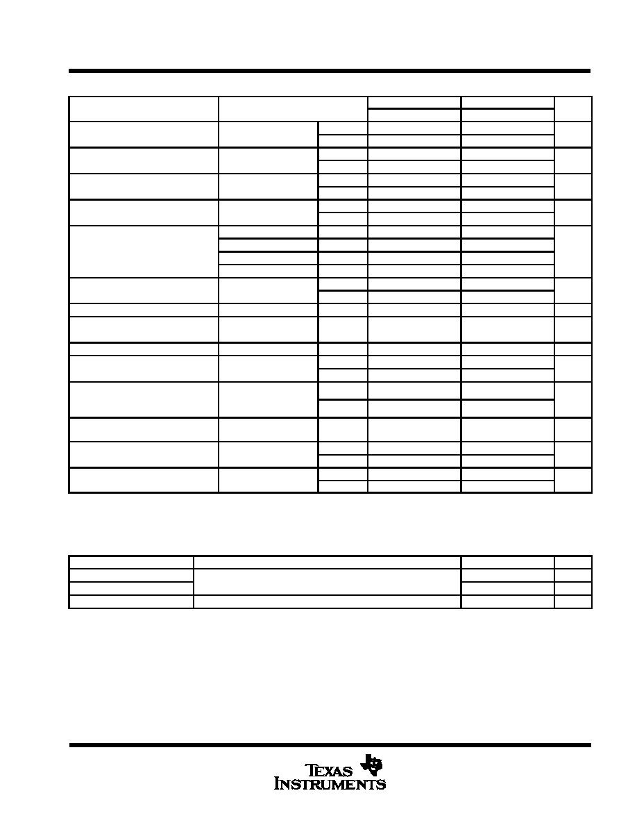
electrical characteristics at specified free-air temperature, V
CC
±
=
±
15 V, C
C
= 30 pF
PARAMETER
TEST CONDITIONS
uA748C
uA748M
UNIT
PARAMETER
TEST CONDITIONS
MIN
TYP
MAX
MIN
TYP
MAX
UNIT
VIO
Input offset voltage
VO = 0
25
∞
C
1
6
1
5
mV
VIO
Input offset voltage
VO = 0
Full range
7.5
6
mV
IIO
Input offset current
VO = 0
25
∞
C
20
200
20
200
nA
IIO
Input offset current
VO = 0
Full range
300
500
nA
IIB
Input bias current
VO = 0
25
∞
C
80
500
80
500
nA
IIB
Input bias current
VO = 0
Full range
800
1500
nA
VICR
Common-mode
25
∞
C
±
12
±
13
±
12
±
13
V
VICR
input voltage range
Full range
±
12
±
12
V
RL= 10 k
25
∞
C
±
12
±
14
±
12
±
14
VO(PP)
Maximum peak
RL
10 k
Full range
±
12
±
12
V
VO(PP)
output voltage swing
RL= 2 k
25
∞
C
±
10
±
13
±
10
±
13
V
RL
2 k
Full range
±
10
±
10
AVD
Large-signal differential
RL
2 k
,
25
∞
C
20
200
50
200
V/mV
AVD
g
g
voltage amplification
VO =
±
10 V
Full range
15
25
V/mV
ri
Input resistance
25
∞
C
0.3
2
0.3
2
M
r
Output resistance
VO = 0,
25
∞
C
75
75
ro
Output resistance
See Note 5
25
∞
C
75
75
Ci
Input capacitance
25
∞
C
1.4
1.4
pF
CMRR
Common-mode
VIC = VICRmin,
25
∞
C
70
90
70
90
dB
CMRR
rejection ratio
VO = 0
Full range
70
70
dB
kSVS
Supply-voltage
sensitivity
VCC =
±
9 V to
±
15 V,
25
∞
C
30
150
30
150
µ
V/V
SVS
sensitivity
(
VIO /
VCC)
CC
VO = 0
Full range
150
150
µ
V/V
IOS
Short-circuit
output current
25
∞
C
±
25
±
40
±
25
±
40
mA
ICC
Supply current
No load
VO = 0
25
∞
C
1.7
2.8
1.7
2.8
mA
ICC
Supply current
No load,
VO = 0
Full range
3.3
3.3
mA
PD
Power dissipation
No load
VO = 0
25
∞
C
50
85
50
85
mW
PD
(each amplifier)
No load,
VO = 0
Full range
100
100
mW
All characteristics are measured under open-loop conditions with zero common-mode input voltage unless otherwise specified. Full range for
uA748C is 0
∞
C to 70
∞
C and for uA748M is ≠ 55
∞
C to 125
∞
C.
NOTE 5: This typical value applies only at frequencies above a few hundred hertz because of the effects of drift and thermal feedback.
operating characteristics, V
CC
±
=
±
15 V, T
A
= 25
∞
C
PARAMETER
TEST CONDITIONS
MIN
TYP
MAX
UNIT
tr
Rise time
VI = 20 mV RL = 2 k
CL = 100 pF CC = 30 pF See Figure 1
0.3
µ
s
Overshoot factor
VI = 20 mV, RL = 2 k
, CL = 100 pF, CC = 30 pF, See Figure 1
5%
SR
Slew rate at unity gain
VI = 10 V, RL = 2 k
, CL = 100 pF, CC = 30 pF, See Figure 1
0.5
V/
µ
s

uA748C, uA748M
GENERAL-PURPOSE OPERATIONAL AMPLIFIERS
SLOS095 ≠ D921, DECEMBER 1970 ≠ REVISED OCTOBER 1990
POST OFFICE BOX 655303
∑
DALLAS, TEXAS 75265
4
PARAMETER MEASUREMENT INFORMATION
VI
0 V
≠
+
Input
COMP
N1
CC = 30 pF
N2 (open)
OUT
RL = 2 k
CL
100 pF
INPUT VOLTAGE
WAVEFORM
TEST CIRCUIT
Figure 1. Rise Time, Overshoot, and Slew Rate
TYPICAL CHARACTERISTICS
≠ 60
0
IIO ≠ Input Offset Current ≠ nA
TA ≠ Free-Air Temperature ≠
∞
C
140
100
≠ 40 ≠ 20
0
20
40
60
80
100 120
20
40
60
80
VCC
±
=
±
15 V
≠ 60
0
IIB ≠ Input Bias Current ≠ nA
TA ≠ Free-Air Temperature ≠
∞
C
140
400
≠ 40 ≠ 20
0
20
40
60
80
100 120
100
200
300
INPUT BIAS CURRENT
vs
FREE-AIR TEMPERATURE
INPUT OFFSET CURRENT
vs
FREE-AIR TEMPERATURE
90
70
50
30
10
I IO
VCC
±
=
±
15 V
350
250
150
50
IBI
œœœœ
œœœœ
uA748C
œœœ
œœœ
uA748C
Figure 2
Figure 3
Data at high and low temperatures are applicably only within the rated operating free-air temperature range of the particular devices.

uA748C, uA748M
GENERAL-PURPOSE OPERATIONAL AMPLIFIERS
SLOS095 ≠ D921, DECEMBER 1970 ≠ REVISED OCTOBER 1990
POST OFFICE BOX 655303
∑
DALLAS, TEXAS 75265
5
TYPICAL CHARACTERISTICS
0.1
VOM ≠ Maximum Peak Output V
oltage ≠ V
RL ≠ Load Resistance ≠ k
±
14
10
±
4
±
5
±
6
±
7
±
8
±
9
±
10
±
11
±
12
±
13
0.2
0.4
0.7 1
2
4
7
VCC
±
=
±
15 V
TA = 25
∞
C
100
f ≠ Frequency ≠ Hz
±
20
1 M
0
±
2
±
4
±
6
±
8
±
10
±
12
±
14
±
16
±
18
1 k
10 k
100 k
MAXIMUM PEAK OUTPUT VOLTAGE
vs
LOAD RESISTANCE
MAXIMUM PEAK OUTPUT VOLTAGE
vs
FREQUENCY
¡¡¡¡¡
¡¡¡¡¡
¡¡¡¡¡
¡¡¡¡¡
RL = 10 k
CC = 30 pF
TA = 25
∞
C
VCC
±
=
±
15 V
¡¡
¡¡
V
OM
VOM ≠ Maximum Peak Output V
oltage ≠ V
¡¡
¡¡
V
OM
Figure 4
Figure 5
1
A
VD ≠ Differential V
oltage
Amplification
f ≠ Frequency ≠ Hz
10 7
100 M
10 ≠ 1
10
100
1 k
10 k 100 k 1 M
10 M
1
101
102
103
104
105
106
VCC
±
=
±
15 V
RL = 2 k
CC = 30 pF
TA = 25
∞
C
0
A
VD ≠ Differential V
oltage
Amplification
V/mV
|VCC
±
| ≠ Supply Voltage ≠ V
400
20
10
2
4
6
8
10
12
14
16
18
200
100
20
40
RL = 2 k
TA = 25
∞
C
OPEN-LOOP LARGE-SIGNAL DIFFERENTIAL
VOLTAGE AMPLIFICATION
vs
FREQUENCY
OPEN-LOOP LARGE-SIGNAL DIFFERENTIAL
VOLTAGE AMPLIFICATION
vs
SUPPLY VOLTAGE
¡¡
¡¡
¡¡
A
VD
¡¡
¡¡
A
VD
Figure 6
Figure 7