 | –≠–ª–µ–∫—Ç—Ä–æ–Ω–Ω—ã–π –∫–æ–º–ø–æ–Ω–µ–Ω—Ç: UA7915C | –°–∫–∞—á–∞—Ç—å:  PDF PDF  ZIP ZIP |
µA7900 SERIES
NEGATIVE VOLTAGE REGULATORS
SLVS058D - JUNE 1976 - REVISED APRIL 2004
1
POST OFFICE BOX 655303
∑
DALLAS, TEXAS 75265
D
3-Terminal Regulators
D
Output Current Up To 1.5 A
D
No External Components
D
Internal Thermal Overload Protection
D
High-Power Dissipation Capability
D
Internal Short-Circuit Current Limiting
D
Output Transistor Safe-Area Compensation
description/ordering information
This series of fixed-negative-voltage
integrated-circuit voltage regulators is designed
to complement Series
µ
A7800 in a wide range of
applications. These applications include on-card
regulation for elimination of noise and distribution
problems associated with single-point regulation. Each of these regulators can deliver up to 1.5 A of output
current. The internal current limiting and thermal shutdown features of these regulators essentially make them
immune to overload. In addition to use as fixed-voltage regulators, these devices can be used with external
components to obtain adjustable output voltages and currents and also as the power-pass element in precision
regulators.
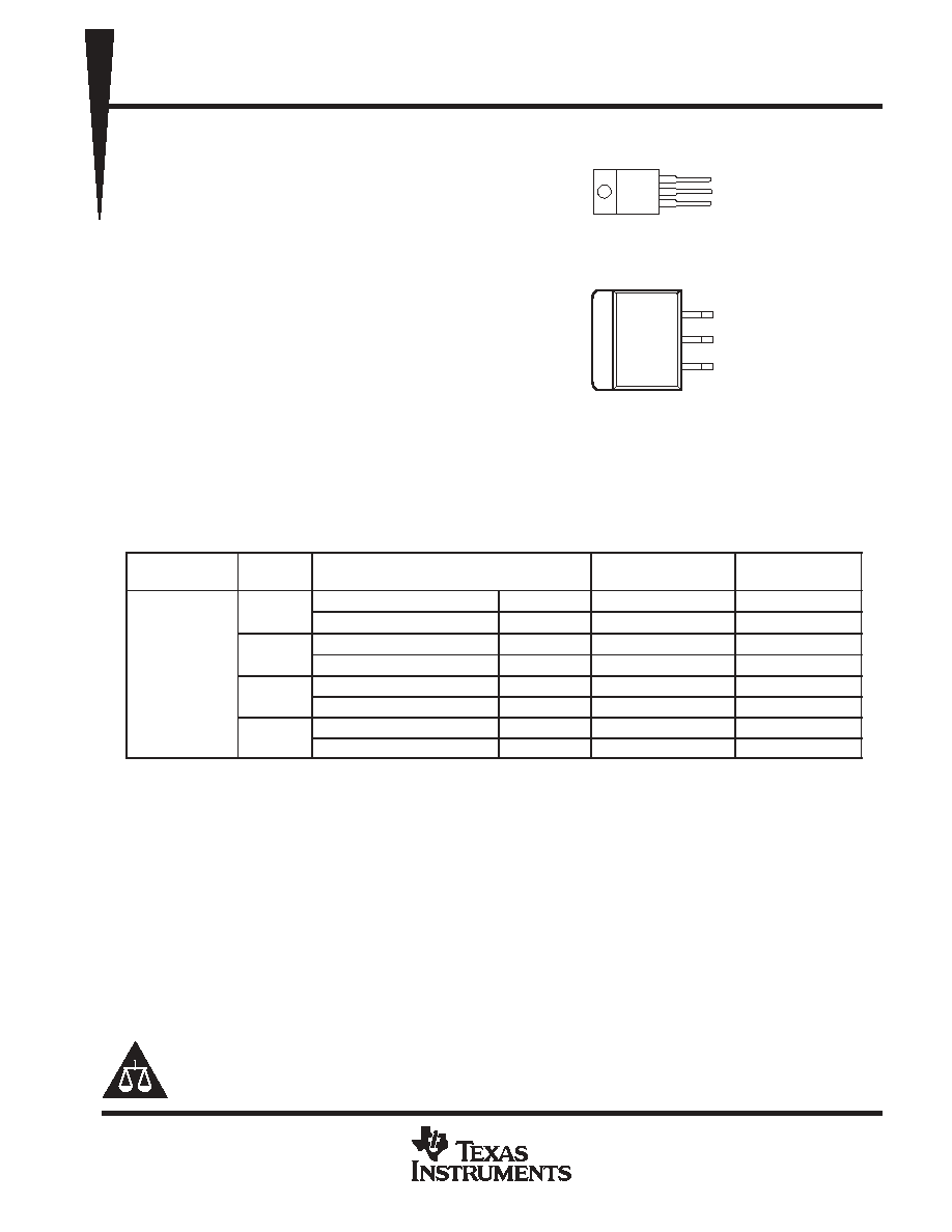
ORDERING INFORMATION
TJ
VO(NOM)
(V)
PACKAGE
ORDERABLE
PART NUMBER
TOP-SIDE
MARKING
-15
Power Flex (KTE)
Reel of 2000
µ
A7915CKTER
µ
A7915C
-15
TO-220, short shoulder (KCS)
Tube of 50
µ
A7915CKCS
µ
A7915C
-12
Power Flex (KTE)
Reel of 2000
µ
A7912CKTER
µ
A7912C
0∞
C to 125
∞
C
-12
TO-220, short shoulder (KCS)
Tube of 50
µ
A7912CKCS
µ
A7912C
0∞
C to 125
∞
C
-8
Power Flex (KTE)
Reel of 2000
µ
A7908CKTER
µ
A7908C
-8
TO-220, short shoulder (KCS)
Tube of 50
µ
A7908CKCS
µ
A7908C
-5
Power Flex (KTE)
Reel of 2000
µ
A7905CKTER
µ
A7905C
-5
TO-220, short shoulder (KCS)
Tube of 50
µ
A7905CKCS
µ
A7905C
Package drawings, standard packing quantities, thermal data, symbolization, and PCB design guidelines are available at
www.ti.com/sc/package.
Please be aware that an important notice concerning availability, standard warranty, and use in critical applications of
Texas Instruments semiconductor products and disclaimers thereto appears at the end of this data sheet.
Copyright
2004, Texas Instruments Incorporated
PRODUCTION DATA information is current as of publication date.
Products conform to specifications per the terms of Texas Instruments
standard warranty. Production processing does not necessarily include
testing of all parameters.
KTE PACKAGE
(TOP VIEW)
OUTPUT
COMMON
INPUT
INPUT
INPUT
OUTPUT
KCS (TO-220) PACKAGE
(TOP VIEW)
COMMON
INPUT
µA7900 SERIES
NEGATIVE VOLTAGE REGULATORS
SLVS058D - JUNE 1976 - REVISED APRIL 2004
2
POST OFFICE BOX 655303
∑
DALLAS, TEXAS 75265
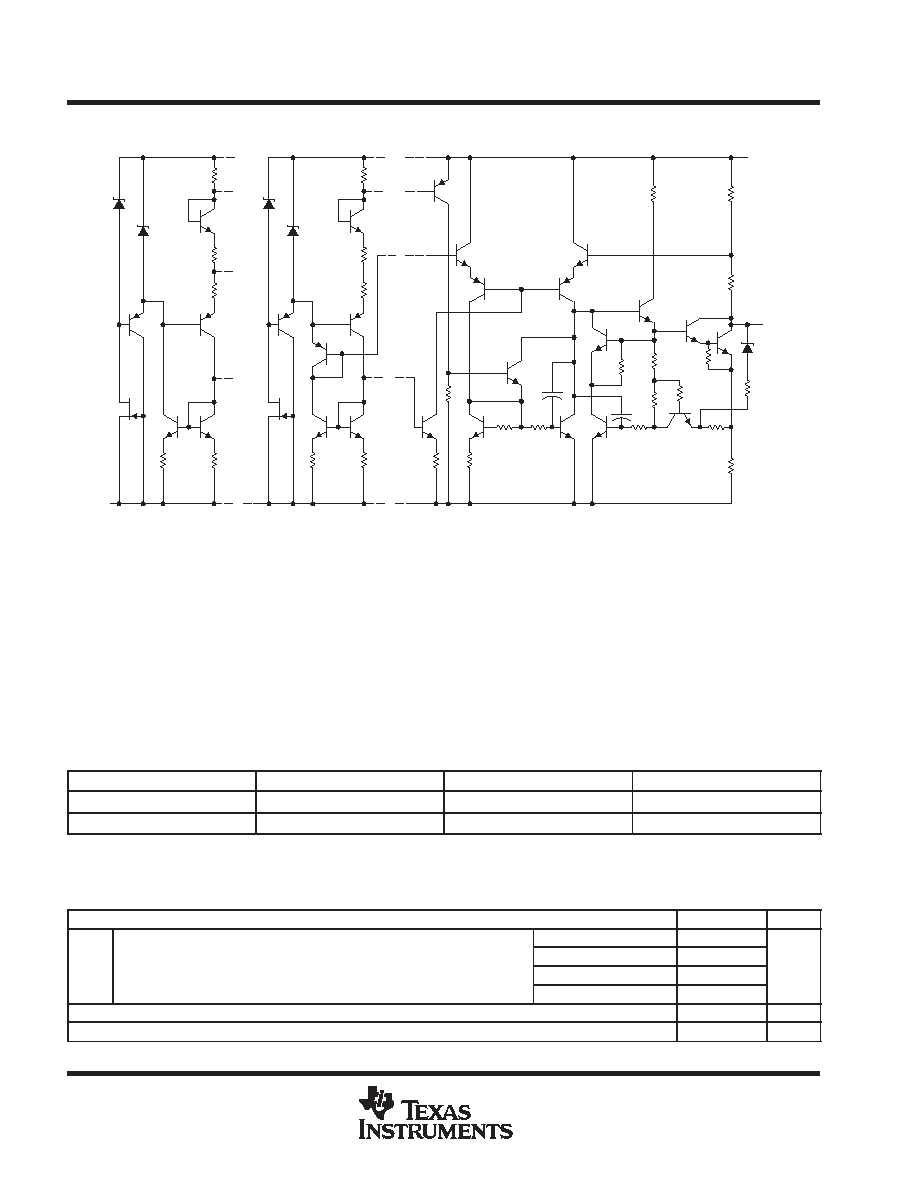
schematic
COMMON
OUTPUT
12 V to 18 V
5 V to 8 V
6.2 V
5 k
20 k
0.2 k
INPUT
All component values are nominal.
absolute maximum ratings over virtual junction temperature range (unless otherwise noted)
Input voltage, V
I
:
µ
A7924C
-40 V
. . . . . . . . . . . . . . . . . . . . . . . . . . . . . . . . . . . . . . . . . . . . . . . . . . . . . . . . . . . . . . . .
All others
-35 V
. . . . . . . . . . . . . . . . . . . . . . . . . . . . . . . . . . . . . . . . . . . . . . . . . . . . . . . . . . . . . . . .
Operating virtual junction temperature, T
J
150
∞
C
. . . . . . . . . . . . . . . . . . . . . . . . . . . . . . . . . . . . . . . . . . . . . . . . . . .
Storage temperature range, T
stg
-65 to 150
∞
C
. . . . . . . . . . . . . . . . . . . . . . . . . . . . . . . . . . . . . . . . . . . . . . . . . . . . .
Stresses beyond those listed under "absolute maximum ratings" may cause permanent damage to the device. These are stress ratings only, and
functional operation of the device at these or any other conditions beyond those indicated under "recommended operating conditions" is not
implied. Exposure to absolute-maximum-rated conditions for extended periods may affect device reliability.
package thermal data (see Note 1)
PACKAGE
BOARD
JC
JA
Power Flex (KTE)
High K, JESD 51-5
3
∞
C/W
23
∞
C/W
TO-220 (KCS)
High K, JESD 51-5
3
∞
C/W
19
∞
C/W
NOTE 1: Maximum power dissipation is a function of TJ(max),
JA, and TA. The maximum allowable power dissipation at any allowable ambient
temperature is PD = (TJ(max) - TA)/
JA. Operating at the absolute maximum TJ of 150
∞
C can affect reliability.
recommended operating conditions
MIN
MAX
UNIT
µ
A7905C
-7
-25
VI
Input voltage
µ
A7908C
-10.5
-25
V
VI
Input voltage
µ
A7912C
-14.5
-30
V
µ
A7915C
-17.5
-30
IO
Output current
1.5
A
TJ
Operating virtual junction temperature
0
125
∞
C
µA7900 SERIES
NEGATIVE VOLTAGE REGULATORS
SLVS058D - JUNE 1976 - REVISED APRIL 2004
3
POST OFFICE BOX 655303
∑
DALLAS, TEXAS 75265
electrical characteristics at specified virtual junction temperature, V
I
= -10 V, I
O
= 500 mA (unless
otherwise noted)
PARAMETER
TEST CONDITIONS
TJ
µ
A7905C
UNITS
PARAMETER
TEST CONDITIONS
TJ
MIN
TYP
MAX
UNITS
25
∞
C
-4.8
-5
-5.2
Output voltage
IO = 5 mA to 1 A,
P
15 W
VI = -7 V to -20 V,
0
∞
C to 125
∞
C
-4.75
-5.25
V
Input regulation
VI = -7 V to -25 V
12.5
50
mV
Input regulation
VI = -8 V to -12 V
4
15
mV
Ripple rejection
VI = -8 V to -18 V,
f = 120 Hz
0
∞
C to 125
∞
C
54
60
dB
Output regulation
IO = 5 mA to 1.5 A
15
100
mV
Output regulation
IO = 250 mA to 750 mA
5
50
mV
Temperature coefficient of output voltage
IO = 5 mA
0
∞
C to 125
∞
C
-0.4
mV/
∞
C
Output noise voltage
f = 10 Hz to 100 kHz
25
∞
C
125
µ
V
Dropout voltage
IO = 1 A
25
∞
C
1.1
V
Bias current
25
∞
C
1.5
2
mA
Bias current change
VI = -7 V to -25 V
0.15
0.5
mA
Bias current change
IO = 5 mA to 1 A
0.08
0.5
mA
Peak output current
25
∞
C
2.1
A
Pulse-testing techniques are used to maintain the junction temperature as close to the ambient temperature as possible. Thermal effects must
be taken into account separately. All characteristics are measured with a 2-
µ
F capacitor across the input and a 1-
µ
F capacitor across the output.
This specification applies only for dc power dissipation permitted by absolute maximum ratings.
electrical characteristics at specified virtual junction temperature, V
I
= -11 V, I
O
= 500 mA (unless
otherwise noted)
PARAMETER
TEST CONDITIONS
TJ
µ
A7906C
UNITS
PARAMETER
TEST CONDITIONS
TJ
MIN
TYP
MAX
UNITS
25
∞
C
-5.75
-6
-6.25
Output voltage
IO = 5 mA to 1 A,
P
15 W
VI = -8 V to -21 V,
0
∞
C to 125
∞
C
-5.7
-6.3
V
Input regulation
VI = -8 V to -25 V
12.5
120
mV
Input regulation
VI = -9 V to -13 V
4
60
mV
Ripple rejection
VI = -9 V to -19 V,
f = 120 Hz
0
∞
C to 125
∞
C
54
60
dB
Output regulation
IO = 5 mA to 1.5 A
15
120
mV
Output regulation
IO = 250 mA to 750 mA
5
60
mV
Temperature coefficient of output voltage
IO = 5 mA
0
∞
C to 125
∞
C
-0.4
mV/
∞
C
Output noise voltage
f = 10 Hz to 100 kHz
25
∞
C
150
µ
V
Dropout voltage
IO = 1 A
25
∞
C
1.1
V
Bias current
25
∞
C
1.5
2
mA
Bias current change
VI = -8 V to -25 V
0.15
1.3
mA
Bias current change
IO = 5 mA to 1 A
0.08
0.5
mA
Peak output current
25
∞
C
2.1
A
Pulse-testing techniques are used to maintain the junction temperature as close to the ambient temperature as possible. Thermal effects must
be taken into account separately. All characteristics are measured with a 2-
µ
F capacitor across the input and a 1-
µ
F capacitor across the output.
This specification applies only for dc power dissipation permitted by absolute maximum ratings.

µA7900 SERIES
NEGATIVE VOLTAGE REGULATORS
SLVS058D - JUNE 1976 - REVISED APRIL 2004
4
POST OFFICE BOX 655303
∑
DALLAS, TEXAS 75265
electrical characteristics at specified virtual junction temperature, V
I
= -14 V, I
O
= 500 mA (unless
otherwise noted)
PARAMETER
TEST CONDITIONS
TJ
µ
A7908C
UNITS
PARAMETER
TEST CONDITIONS
TJ
MIN
TYP
MAX
UNITS
25
∞
C
-7.7
-8
-8.3
Output voltage
IO = 5 mA to 1 A,
P
15 W
VI = -10.5 V to -23 V,
0
∞
C to 125
∞
C
-7.6
-8.4
V
Input regulation
VI = -10.5 V to -25 V
12.5
160
mV
Input regulation
VI = -11 V to -17 V
4
80
mV
Ripple rejection
VI = -11.5 V to -21.5 V, f = 120 Hz
0
∞
C to 125
∞
C
54
60
dB
Output regulation
IO = 5 mA to 1.5 A
15
160
mV
Output regulation
IO = 250 mA to 750 mA
5
80
mV
Temperature coefficient of output voltage
IO = 5 mA
0
∞
C to 125
∞
C
-0.6
mV/
∞
C
Output noise voltage
f = 10 Hz to 100 kHz
25
∞
C
200
µ
V
Dropout voltage
IO = 1 A
25
∞
C
1.1
V
Bias current
25
∞
C
1.5
2
mA
Bias current change
VI = -10.5 V to -25 V
0.15
1
mA
Bias current change
IO = 5 mA to 1 A
0.08
0.5
mA
Peak output current
25
∞
C
2.1
A
Pulse-testing techniques are used to maintain the junction temperature as close to the ambient temperature as possible. Thermal effects must
be taken into account separately. All characteristics are measured with a 2-
µ
F capacitor across the input and a 1-
µ
F capacitor across the output.
This specification applies only for dc power dissipation permitted by absolute maximum ratings.
electrical characteristics at specified virtual junction temperature, V
I
= -19 V, I
O
= 500 mA (unless
otherwise noted)
PARAMETER
TEST CONDITIONS
TJ
µ
A7912C
UNITS
PARAMETER
TEST CONDITIONS
TJ
MIN
TYP
MAX
UNITS
25
∞
C
-11.5
-12
-12.5
Output voltage
IO = 5 mA to 1 A,
P
15 W
VI = -14.5 V to -27 V,
0
∞
C to 125
∞
C
-11.4
-12.6
V
Input regulation
VI = -14.5 V to -30 V
5
80
mV
Input regulation
VI = -16 V to -22 V
3
30
mV
Ripple rejection
VI = -15 V to -25 V, f = 120 Hz
0
∞
C to 125
∞
C
54
60
dB
Output regulation
IO = 5 mA to 1.5 A
15
200
mV
Output regulation
IO = 250 mA to 750 mA
5
75
mV
Temperature coefficient of output voltage
IO = 5 mA
0
∞
C to 125
∞
C
-0.8
mV/
∞
C
Output noise voltage
f = 10 Hz to 100 kHz
25
∞
C
300
µ
V
Dropout voltage
IO = 1 A
25
∞
C
1.1
V
Bias current
25
∞
C
2
3
mA
Bias current change
VI = -14.5 V to -30 V
0.04
0.5
mA
Bias current change
IO = 5 mA to 1 A
0.06
0.5
mA
Peak output current
25
∞
C
2.1
A
Pulse-testing techniques are used to maintain the junction temperature as close to the ambient temperature as possible. Thermal effects must
be taken into account separately. All characteristics are measured with a 2-
µ
F capacitor across the input and a 1-
µ
F capacitor across the output.
This specification applies only for dc power dissipation permitted by absolute maximum ratings.

µA7900 SERIES
NEGATIVE VOLTAGE REGULATORS
SLVS058D - JUNE 1976 - REVISED APRIL 2004
5
POST OFFICE BOX 655303
∑
DALLAS, TEXAS 75265
electrical characteristics at specified virtual junction temperature, V
I
= -23 V, I
O
= 500 mA (unless
otherwise noted)
PARAMETER
TEST CONDITIONS
TJ
µ
A7915C
UNITS
PARAMETER
TEST CONDITIONS
TJ
MIN
TYP
MAX
UNITS
25
∞
C
-14.4
-15
-15.6
Output voltage
IO = 5 mA to 1 A,
P
15 W
VI = -17.5 V to -30 V,
0
∞
C to 125
∞
C
-14.25
-15.75
V
Input regulation
VI = -17.5 V to -30 V
5
100
mV
Input regulation
VI = -20 V to -26 V
3
50
mV
Ripple rejection
VI = -18.5 V to -28.5 V, f = 120 Hz
0
∞
C to 125
∞
C
54
60
dB
Output regulation
IO = 5 mA to 1.5 A
20
300
mV
Output regulation
IO = 250 mA to 750 mA
8
150
mV
Temperature coefficient of output voltage
IO = 5 mA
0
∞
C to 125
∞
C
-1
mV/
∞
C
Output noise voltage
f = 10 Hz to 100 kHz
25
∞
C
375
µ
V
Dropout voltage
IO = 1 A
25
∞
C
1.1
V
Bias current
25
∞
C
2
3
mA
Bias current change
VI = -17.5 V to -30 V
0.04
0.5
mA
Bias current change
IO = 5 mA to 1 A
0.06
0.5
mA
Peak output current
25
∞
C
2.1
A
Pulse-testing techniques are used to maintain the junction temperature as close to the ambient temperature as possible. Thermal effects must
be taken into account separately. All characteristics are measured with a 2-
µ
F capacitor across the input and a 1-
µ
F capacitor across the output.
This specification applies only for dc power dissipation permitted by absolute maximum ratings.
electrical characteristics at specified virtual junction temperature, V
I
= -27 V, I
O
= 500 mA (unless
otherwise noted)
PARAMETER
TEST CONDITIONS
TJ
µ
A7918C
UNITS
PARAMETER
TEST CONDITIONS
TJ
MIN
TYP
MAX
UNITS
25
∞
C
-17.3
-18
-18.7
Output voltage
IO = 5 mA to 1 A,
P
15 W
VI = -21 V to -33 V,
0
∞
C to 125
∞
C
-17.1
-18.9
V
Input regulation
VI = -21 V to -33 V
5
360
mV
Input regulation
VI = -24 V to -30 V
3
180
mV
Ripple rejection
VI = -22 V to -32 V, f = 120 Hz
0
∞
C to 125
∞
C
54
60
dB
Output regulation
IO = 5 mA to 1.5 A
30
360
mV
Output regulation
IO = 250 mA to 750 mA
10
180
mV
Temperature coefficient of output voltage
IO = 5 mA
0
∞
C to 125
∞
C
-1
mV/
∞
C
Output noise voltage
f = 10 Hz to 100 kHz
25
∞
C
450
µ
V
Dropout voltage
IO = 1 A
25
∞
C
1.1
V
Bias current
25
∞
C
2
3
mA
Bias current change
VI = -21 V to -33 V
0.04
1
mA
Bias current change
IO = 5 mA to 1 A
0.06
0.5
mA
Peak output current
25
∞
C
2.1
A
Pulse-testing techniques are used to maintain the junction temperature as close to the ambient temperature as possible. Thermal effects must
be taken into account separately. All characteristics are measured with a 2-
µ
F capacitor across the input and a 1-
µ
F capacitor across the output.
This specification applies only for dc power dissipation permitted by absolute maximum ratings.
µA7900 SERIES
NEGATIVE VOLTAGE REGULATORS
SLVS058D - JUNE 1976 - REVISED APRIL 2004
6
POST OFFICE BOX 655303
∑
DALLAS, TEXAS 75265
electrical characteristics at specified virtual junction temperature, V
I
= -33 V, I
O
= 500 mA (unless
otherwise noted)
PARAMETER
TEST CONDITIONS
TJ
µ
A7924C
UNITS
PARAMETER
TEST CONDITIONS
TJ
MIN
TYP
MAX
UNITS
25
∞
C
-23
-24
-25
Output voltage
IO = 5 mA to 1 A,
P
15 W
VI = -27 V to -38 V,
0
∞
C to 125
∞
C
-22.8
-25.2
V
Input regulation
VI = -27 V to -38 V
5
480
mV
Input regulation
VI = -30 V to -36 V
3
240
mV
Ripple rejection
VI = -28 V to -38 V, f = 120 Hz
0
∞
C to 125
∞
C
54
60
dB
Output regulation
IO = 5 mA to 1.5 A
85
480
mV
Output regulation
IO = 250 mA to 750 mA
25
240
mV
Temperature coefficient of output voltage
IO = 5 mA
0
∞
C to 125
∞
C
-1
mV/
∞
C
Output noise voltage
f = 10 Hz to 100 kHz
25
∞
C
600
µ
V
Dropout voltage
IO = 1 A
25
∞
C
1.1
V
Bias current
25
∞
C
2
3
mA
Bias current change
VI = -27 V to -38 V
0.04
1
mA
Bias current change
IO = 5 mA to 1 A
0.06
0.5
mA
Peak output current
25
∞
C
2.1
A
Pulse-testing techniques are used to maintain the junction temperature as close to the ambient temperature as possible. Thermal effects must
be taken into account separately. All characteristics are measured with a 2-
µ
F capacitor across the input and a 1-
µ
F capacitor across the output.
This specification applies only for dc power dissipation permitted by absolute maximum ratings.
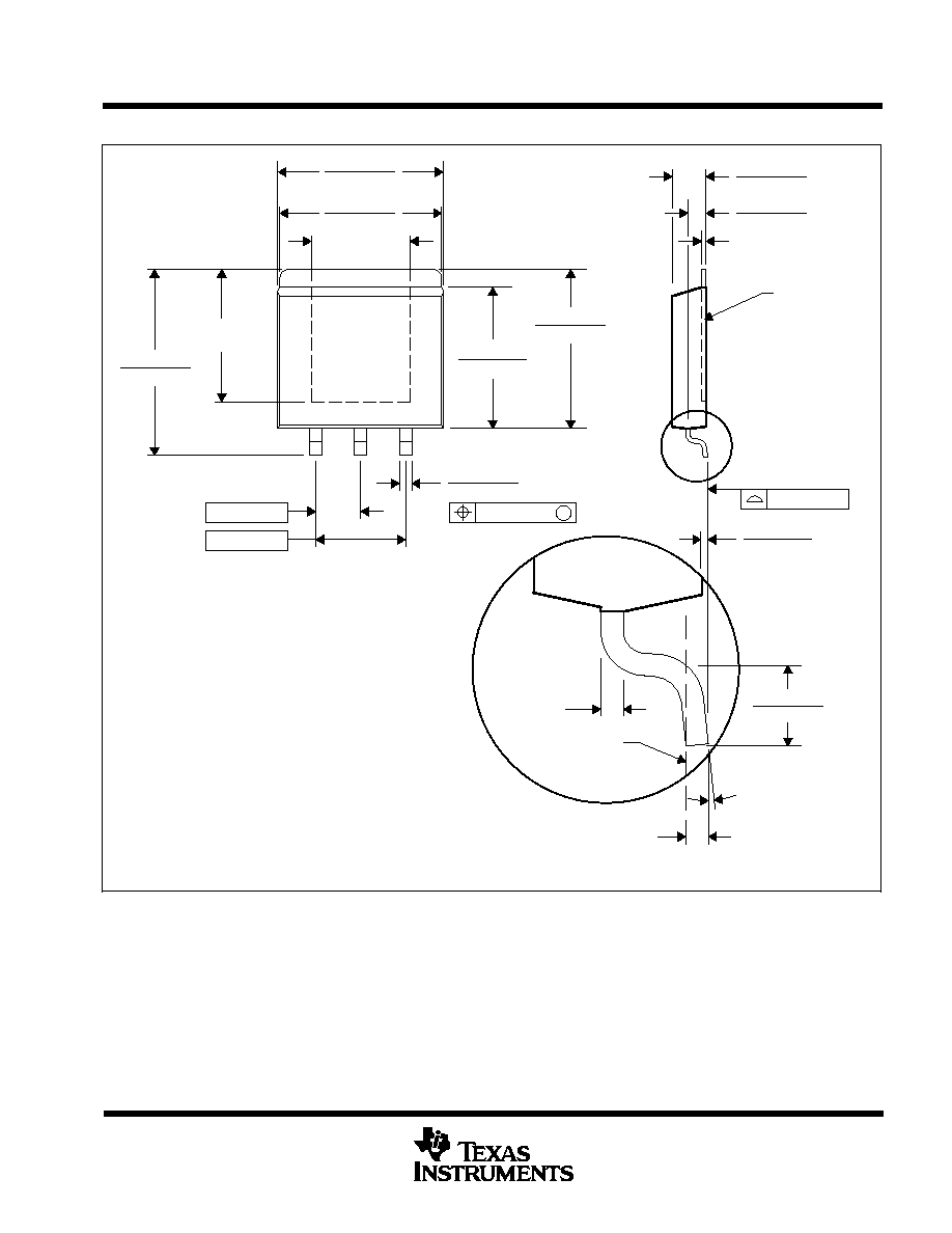
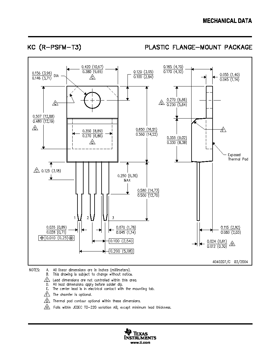
MECHANICAL DATA
MPFM001E ≠ OCTOBER 1994 ≠ REVISED JANUARY 2001
1
POST OFFICE BOX 655303
∑
DALLAS, TEXAS 75265
KTE (R-PSFM-G3)
PowerFLEX
TM
PLASTIC FLANGE-MOUNT
0.360 (9,14)
0.350 (8,89)
0.080 (2,03)
0.070 (1,78)
0.010 (0,25) NOM
0.040 (1,02)
Seating Plane
0.050 (1,27)
0.001 (0,03)
0.005 (0,13)
0.010 (0,25)
NOM
Gage Plane
0.010 (0,25)
0.031 (0,79)
0.041 (1,04)
4073375/F 12/00
NOM
3
1
0.350 (8,89)
0.220 (5,59)
0.360 (9,14)
0.295 (7,49)
NOM
0.320 (8,13)
0.310 (7,87)
0.025 (0,63)
0.031 (0,79)
Thermal Tab
(See Note C)
0.004 (0,10)
M
0.010 (0,25)
0.100 (2,54)
3
∞
≠ 6
∞
0.410 (10,41)
0.420 (10,67)
0.200 (5,08)
0.365 (9,27)
0.375 (9,52)
NOTES: A. All linear dimensions are in inches (millimeters).
B. This drawing is subject to change without notice.
C. The center lead is in electrical contact with the thermal tab.
D. Dimensions do not include mold protrusions, not to exceed 0.006 (0,15).
E. Falls within JEDEC MO-169
PowerFLEX is a trademark of Texas Instruments.


IMPORTANT NOTICE
Texas Instruments Incorporated and its subsidiaries (TI) reserve the right to make corrections, modifications,
enhancements, improvements, and other changes to its products and services at any time and to discontinue
any product or service without notice. Customers should obtain the latest relevant information before placing
orders and should verify that such information is current and complete. All products are sold subject to TI's terms
and conditions of sale supplied at the time of order acknowledgment.
TI warrants performance of its hardware products to the specifications applicable at the time of sale in
accordance with TI's standard warranty. Testing and other quality control techniques are used to the extent TI
deems necessary to support this warranty. Except where mandated by government requirements, testing of all
parameters of each product is not necessarily performed.
TI assumes no liability for applications assistance or customer product design. Customers are responsible for
their products and applications using TI components. To minimize the risks associated with customer products
and applications, customers should provide adequate design and operating safeguards.
TI does not warrant or represent that any license, either express or implied, is granted under any TI patent right,
copyright, mask work right, or other TI intellectual property right relating to any combination, machine, or process
in which TI products or services are used. Information published by TI regarding third-party products or services
does not constitute a license from TI to use such products or services or a warranty or endorsement thereof.
Use of such information may require a license from a third party under the patents or other intellectual property
of the third party, or a license from TI under the patents or other intellectual property of TI.
Reproduction of information in TI data books or data sheets is permissible only if reproduction is without
alteration and is accompanied by all associated warranties, conditions, limitations, and notices. Reproduction
of this information with alteration is an unfair and deceptive business practice. TI is not responsible or liable for
such altered documentation.
Resale of TI products or services with statements different from or beyond the parameters stated by TI for that
product or service voids all express and any implied warranties for the associated TI product or service and
is an unfair and deceptive business practice. TI is not responsible or liable for any such statements.
Following are URLs where you can obtain information on other Texas Instruments products and application
solutions:
Products
Applications
Amplifiers
amplifier.ti.com
Audio
www.ti.com/audio
Data Converters
dataconverter.ti.com
Automotive
www.ti.com/automotive
DSP
dsp.ti.com
Broadband
www.ti.com/broadband
Interface
interface.ti.com
Digital Control
www.ti.com/digitalcontrol
Logic
logic.ti.com
Military
www.ti.com/military
Power Mgmt
power.ti.com
Optical Networking
www.ti.com/opticalnetwork
Microcontrollers
microcontroller.ti.com
Security
www.ti.com/security
Telephony
www.ti.com/telephony
Video & Imaging
www.ti.com/video
Wireless
www.ti.com/wireless
Mailing Address:
Texas Instruments
Post Office Box 655303 Dallas, Texas 75265
Copyright
2004, Texas Instruments Incorporated