 | –≠–ª–µ–∫—Ç—Ä–æ–Ω–Ω—ã–π –∫–æ–º–ø–æ–Ω–µ–Ω—Ç: UA79M08C | –°–∫–∞—á–∞—Ç—å:  PDF PDF  ZIP ZIP |
µ
A79M00 SERIES
NEGATIVE-VOLTAGE REGULATORS
SLVS060J ≠ JUNE 1976 ≠ REVISED MAY 2003
1
POST OFFICE BOX 655303
∑
DALLAS, TEXAS 75265
D
3-Terminal Regulators
D
Output Current Up To 500 mA
D
No External Components
D
High Power-Dissipation Capability
D
Internal Short-Circuit Current Limiting
D
Output Transistor Safe-Area Compensation
µ
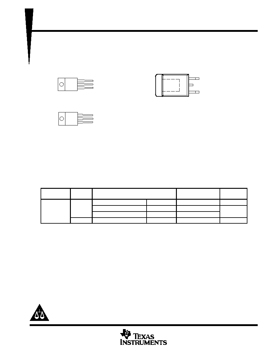
A79M05,
µ
A79M08 . . . KTP PACKAGE
(TOP VIEW)
OUTPUT
INPUT
COMMON
INPUT
OUTPUT
µ
A79M05 . . . KC (TO-220) PACKAGE
(TOP VIEW)
COMMON
INPUT
INPUT
OUTPUT
µ
A79M05 . . . KCS (TO-220) PACKAGE
(TOP VIEW)
COMMON
INPUT
INPUT
description/ordering information
This series of fixed-negative-voltage integrated-circuit voltage regulators is designed to complement the
µ
A78M00 series in a wide range of applications. These applications include on-card regulation for elimination
of noise and distribution problems associated with single-point regulation. Each of these regulators delivers up
to 500 mA of output current. The internal current-limiting and thermal-shutdown features of these regulators
essentially make them immune to overload. In addition to use as fixed-voltage regulators, these devices can
be used with external components to obtain adjustable output voltages and currents, and also as the
power-pass element in precision regulators.
ORDERING INFORMATION
TJ
VO(NOM)
(V)
PACKAGE
ORDERABLE
PART NUMBER
TOP-SIDE
MARKING
Power Flex (KTP)
Reel of 3000
µ
A79M05CKTPR
µ
A79M05C
0
∞
C to 125
∞
C
≠5
TO-220 (KC)
Tube of 50
µ
A79M05CKC
µ
A79M05C
0
∞
C to 125
∞
C
TO-220, short shoulder (KCS)
Tube of 20
µ
A79M05CKCS
µ
A79M05C
≠8
Power Flex (KTP)
Reel of 3000
µ
A79M08CKTPR
µ
A79M08C
Package drawings, standard packing quantities, thermal data, symbolization, and PCB design guidelines are available at
www.ti.com/sc/package.
Please be aware that an important notice concerning availability, standard warranty, and use in critical applications of
Texas Instruments semiconductor products and disclaimers thereto appears at the end of this data sheet.
Copyright
2003, Texas Instruments Incorporated
PRODUCTION DATA information is current as of publication date.
Products conform to specifications per the terms of Texas Instruments
standard warranty. Production processing does not necessarily include
testing of all parameters.
µ
A79M00 SERIES
NEGATIVE-VOLTAGE REGULATORS
SLVS060J ≠ JUNE 1976 ≠ REVISED MAY 2003
2
POST OFFICE BOX 655303
∑
DALLAS, TEXAS 75265
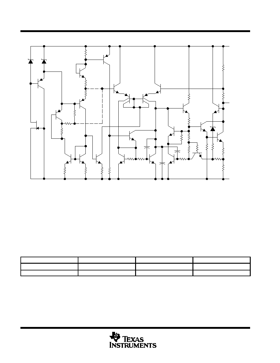
schematic
4.5 k
to 6.3 k
COMMON
OUTPUT
INPUT
0.1
0.2
1.7 k
to 18 k
Resistor values shown are nominal.
absolute maximum ratings over virtual junction temperature range (unless otherwise noted)
Input voltage, V
I
35 V
. . . . . . . . . . . . . . . . . . . . . . . . . . . . . . . . . . . . . . . . . . . . . . . . . . . . . . . . . . . . . . . . . . . . . . . . . . .
Operating virtual junction temperature, T
J
150
∞
C
. . . . . . . . . . . . . . . . . . . . . . . . . . . . . . . . . . . . . . . . . . . . . . . . . . .
Lead temperature 1,6 mm (1/16 inch) from case for 10 seconds
260
∞
C
. . . . . . . . . . . . . . . . . . . . . . . . . . . . . . .
Storage temperature range, T
stg
≠65
∞
C to 150
∞
C
. . . . . . . . . . . . . . . . . . . . . . . . . . . . . . . . . . . . . . . . . . . . . . . . . . . .
Stresses beyond those listed under "absolute maximum ratings" may cause permanent damage to the device. These are stress ratings only, and
functional operation of the device at these or any other conditions beyond those indicated under "recommended operating conditions" is not
implied. Exposure to absolute-maximum-rated conditions for extended periods may affect device reliability.
package thermal data (see Note 1)
PACKAGE
BOARD
JC
JA
POWER-FLEX (KTP)
High K, JESD 51-5
19
∞
C/W
28
∞
C/W
TO-220 (KC/KCS)
High K, JESD 51-5
3
∞
C/W
19
∞
C/W
NOTE 1: Maximum power dissipation is a function of TJ(max),
JA, and TA. The maximum allowable power dissipation at any allowable ambient
temperature is PD = (TJ(max) ≠ TA)/
JA. Operating at the absolute maximum TJ of 150
∞
C can affect reliability.
µ
A79M00 SERIES
NEGATIVE-VOLTAGE REGULATORS
SLVS060J ≠ JUNE 1976 ≠ REVISED MAY 2003
3
POST OFFICE BOX 655303
∑
DALLAS, TEXAS 75265
recommended operating conditions
MIN
MAX
UNIT
VI
Input voltage
µ
A79M05C
≠7
≠25
V
VI
Input voltage
µ
A79M08C
≠10.5
≠25
V
IO
Output current
500
mA
TJ
Operating virtual junction temperature
0
125
∞
C
electrical characteristics at specified virtual junction temperature, V
I
= ≠10 V, I
O
= 350 mA, T
J
= 25
∞
C
(unless otherwise noted)
PARAMETER
TEST CONDITIONS
µ
A79M05C
UNIT
PARAMETER
TEST CONDITIONS
MIN
TYP
MAX
UNIT
Output voltage
VI = 7 V to 25 V
IO = 5 mA to 350 mA
≠4.8
≠5
≠5.2
V
Output voltage
VI = ≠7 V to ≠25 V,
IO = 5 mA to 350 mA
TJ = 0
∞
C to 125
∞
C
≠4.75
≠5.25
V
Input voltage regulation
VI = ≠7 V to ≠25 V
7
50
mV
Input voltage regulation
VI = ≠8 V to ≠18 V
3
30
mV
Ripple rejection
VI = ≠8 V to ≠18 V,
IO = 100 mA,
TJ = 0
∞
C to 125
∞
C
50
dB
Ripple rejection
I
,
f = 120 Hz
IO = 300 mA
54
60
dB
Output voltage regulation
IO = 5 mA to 500 mA
75
100
mV
Output voltage regulation
IO = 5 mA to 350 mA
50
mV
Temperature coefficient
of output voltage
IO = 5 mA,
TJ = 0
∞
C to 125
∞
C
≠0.4
mV/
∞
C
Output noise voltage
f = 10 Hz to 100 kHz
125
µ
V
Dropout voltage
1.1
V
Bias current
1
2
mA
Bias current change
VI = ≠8 V to ≠18 V,
TJ = 0
∞
C to 125
∞
C
0.4
mA
Bias current change
IO = 5 mA to 350 mA,
TJ = 0
∞
C to 125
∞
C
0.4
mA
Short-circuit output current
VI = ≠30 V
140
mA
Peak output current
0.65
A
Pulse-testing techniques maintain TJ as close to TA as possible. Thermal effects must be taken into account separately. All characteristics are
measured with a 2-
µ
F capacitor across the input and a 1-
µ
F capacitor across the output.
µ
A79M00 SERIES
NEGATIVE-VOLTAGE REGULATORS
SLVS060J ≠ JUNE 1976 ≠ REVISED MAY 2003
4
POST OFFICE BOX 655303
∑
DALLAS, TEXAS 75265
electrical characteristics at specified virtual junction temperature, V
I
= ≠19 V, I
O
= 350 mA, T
J
= 25
∞
C
(unless otherwise noted)
PARAMETER
TEST CONDITIONS
µ
A79M08C
UNIT
PARAMETER
TEST CONDITIONS
MIN
TYP
MAX
UNIT
Output voltage
VI = 10 5 V to 25 V
IO = 5 mA to 350 mA
≠7.7
≠8
≠8.3
V
Output voltage
VI = ≠10.5 V to ≠25 V,
IO = 5 mA to 350 mA
TJ = 0
∞
C to 125
∞
C
≠7.6
≠8.4
V
Input voltage regulation
VI = ≠10.5 V to ≠25 V
8
80
mV
Input voltage regulation
VI = ≠11 V to ≠21 V
4
50
mV
Ripple rejection
VI = ≠11.5 V to ≠21.5 V,
IO = 100 mA,
TJ = 0
∞
C to 125
∞
C
50
dB
Ripple rejection
I
,
f = 120 Hz
IO = 300 mA
54
59
dB
Output voltage regulation
IO = 5 mA to 500 mA
90
160
mV
Output voltage regulation
IO = 5 mA to 350 mA
60
mV
Temperature coefficient
of output voltage
IO = 5 mA,
TJ = 0
∞
C to 125
∞
C
≠0.6
mV/
∞
C
Output noise voltage
f = 10 Hz to 100 kHz
200
µ
V
Dropout voltage
IO = 5 mA
1.1
V
Bias current
1
2
mA
Bias current change
VI = ≠10.5 V to ≠25 V,
TJ = 0
∞
C to 125
∞
C
0.4
mA
Bias current change
IO = 5 mA to 350 mA,
TJ = 0
∞
C to 125
∞
C
0.4
mA
Short-circuit output current
VI = ≠30 V
140
mA
Peak output current
0.65
A
Pulse-testing techniques maintain TJ as close to TA as possible. Thermal effects must be taken into account separately. All characteristics are
measured with a 2-
µ
F capacitor across the input and a 1-
µ
F capacitor across the output.
PACKAGING INFORMATION
Orderable Device
Status
(1)
Package
Type
Package
Drawing
Pins Package
Qty
Eco Plan
(2)
Lead/Ball Finish
MSL Peak Temp
(3)
7704001HA
OBSOLETE
CFP
U
10
None
Call TI
Call TI
UA79M05CKC
ACTIVE
TO-220
KC
3
50
None
Call TI
Level-1-220C-UNLIM
UA79M05CKCS
ACTIVE
TO-220
KCS
3
50
None
Call TI
Level-NC-NC-NC
UA79M05CKTPR
ACTIVE
PFM
KTP
2
3000
None
Call TI
Level-1-220C-UNLIM
UA79M05MUB
OBSOLETE
CFP
U
10
None
Call TI
Call TI
UA79M06CKTPR
OBSOLETE
PFM
KTP
2
None
Call TI
Call TI
UA79M08CKC
OBSOLETE
TO-220
KC
3
None
Call TI
Call TI
UA79M08CKTPR
ACTIVE
PFM
KTP
2
3000
None
Call TI
Level-1-220C-UNLIM
UA79M12CKC
OBSOLETE
TO-220
KC
3
None
Call TI
Call TI
UA79M12CKTPR
OBSOLETE
PFM
KTP
2
None
Call TI
Call TI
UA79M15CKC
OBSOLETE
TO-220
KC
3
None
Call TI
Call TI
UA79M15CKTPR
OBSOLETE
PFM
KTP
2
None
Call TI
Call TI
UA79M20CKTPR
OBSOLETE
PFM
KTP
2
None
Call TI
Call TI
UA79M24CKTPR
OBSOLETE
PFM
KTP
2
None
Call TI
Call TI
(1)
The marketing status values are defined as follows:
ACTIVE: Product device recommended for new designs.
LIFEBUY: TI has announced that the device will be discontinued, and a lifetime-buy period is in effect.
NRND: Not recommended for new designs. Device is in production to support existing customers, but TI does not recommend using this part in
a new design.
PREVIEW: Device has been announced but is not in production. Samples may or may not be available.
OBSOLETE: TI has discontinued the production of the device.
(2)
Eco Plan - May not be currently available - please check
http://www.ti.com/productcontent
for the latest availability information and additional
product content details.
None: Not yet available Lead (Pb-Free).
Pb-Free (RoHS): TI's terms "Lead-Free" or "Pb-Free" mean semiconductor products that are compatible with the current RoHS requirements
for all 6 substances, including the requirement that lead not exceed 0.1% by weight in homogeneous materials. Where designed to be soldered
at high temperatures, TI Pb-Free products are suitable for use in specified lead-free processes.
Green (RoHS & no Sb/Br): TI defines "Green" to mean "Pb-Free" and in addition, uses package materials that do not contain halogens,
including bromine (Br) or antimony (Sb) above 0.1% of total product weight.
(3)
MSL, Peak Temp. -- The Moisture Sensitivity Level rating according to the JEDECindustry standard classifications, and peak solder
temperature.
Important Information and Disclaimer:The information provided on this page represents TI's knowledge and belief as of the date that it is
provided. TI bases its knowledge and belief on information provided by third parties, and makes no representation or warranty as to the
accuracy of such information. Efforts are underway to better integrate information from third parties. TI has taken and continues to take
reasonable steps to provide representative and accurate information but may not have conducted destructive testing or chemical analysis on
incoming materials and chemicals. TI and TI suppliers consider certain information to be proprietary, and thus CAS numbers and other limited
information may not be available for release.
In no event shall TI's liability arising out of such information exceed the total purchase price of the TI part(s) at issue in this document sold by TI
to Customer on an annual basis.
PACKAGE OPTION ADDENDUM
www.ti.com
11-Feb-2005
Addendum-Page 1