 | –≠–ª–µ–∫—Ç—Ä–æ–Ω–Ω—ã–π –∫–æ–º–ø–æ–Ω–µ–Ω—Ç: UA9636AC | –°–∫–∞—á–∞—Ç—å:  PDF PDF  ZIP ZIP |
uA9636AC
DUAL LINE DRIVER WITH ADJUSTABLE SLEW RATE
SLLS110B ≠ OCTOBER 1980 ≠ REVISED MAY 1995
1
POST OFFICE BOX 655303
∑
DALLAS, TEXAS 75265
D
Meets or Exceeds the Requirements of
ANSI Standards EIA/TIA-423-B and -232-E
and ITU Recommendations V.10 and V.28
D
Output Slew Rate Control
D
Output Short-Circuit-Current Limiting
D
Wide Supply Voltage Range
D
8-Pin Package
D
Designed to Be Interchangeable With
National DS9636A
description
The uA9636AC is a dual, single-ended line driver designed to meet ANSI Standards EIA/TIA-423-B and
EIA/TIA-232-E and ITU Recommendations V.10 and V.28. The slew rates of both amplifiers are controlled by
a single external resistor, R
(WS)
, connected between the wave-shape-control (W-S) terminal and GND. Output
current limiting is provided. Inputs are compatible with TTL and CMOS and are diode protected against negative
transients. This device operates from
±
12 V and is supplied in an 8-pin package.
The uA9636AC is characterized for operation from 0
∞
C to 70
∞
C.
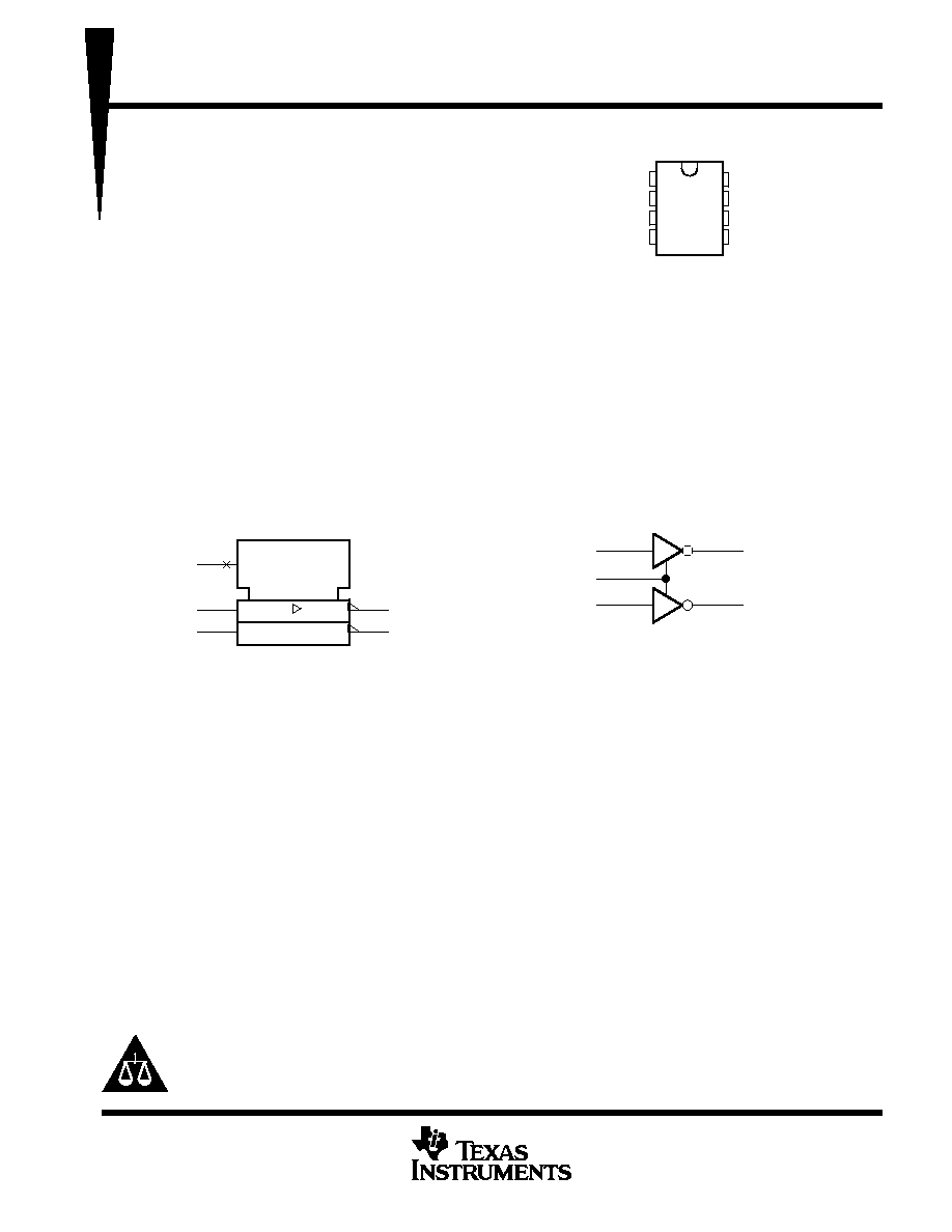
logic symbol
7
6
1
2
3
W-S
1A
2A
1Y
2Y
[Slew-Rate]
This symbol is in accordance with ANSI/IEEE Std 91-1984
and IEC Publication 617-12.
logic diagram
7
1Y
6
2Y
2
1A
3
2A
W-S
1
Copyright
©
1995, Texas Instruments Incorporated
PRODUCTION DATA information is current as of publication date.
Products conform to specifications per the terms of Texas Instruments
standard warranty. Production processing does not necessarily include
testing of all parameters.
Please be aware that an important notice concerning availability, standard warranty, and use in critical applications of
Texas Instruments semiconductor products and disclaimers thereto appears at the end of this data sheet.
1
2
3
4
8
7
6
5
W-S
1A
2A
GND
V
CC+
1Y
2Y
V
CC ≠
D OR P PACKAGE
(TOP VIEW)

uA9636AC
DUAL LINE DRIVER WITH ADJUSTABLE SLEW RATE
SLLS110B ≠ OCTOBER 1980 ≠ REVISED MAY 1995
2
POST OFFICE BOX 655303
∑
DALLAS, TEXAS 75265
schematics of inputs and outputs
VCC
+
EQUIVALENT OF EACH INPUT
TYPICAL OF ALL OUTPUTS
Input
VCC
±
Current
Source
Current
Source
VCC
+
Output
VCC
±
absolute maximum ratings over operating free-air temperature range (unless otherwise noted)
Positive supply voltage range, V
CC+
(see Note 1)
V
CC ≠
to 15 V
. . . . . . . . . . . . . . . . . . . . . . . . . . . . . . . . . . . . . .
Negative supply voltage range, V
CC ≠
0.5 V to ≠ 15 V
. . . . . . . . . . . . . . . . . . . . . . . . . . . . . . . . . . . . . . . . . . . . . . .
Output voltage, V
O
±
15 V
. . . . . . . . . . . . . . . . . . . . . . . . . . . . . . . . . . . . . . . . . . . . . . . . . . . . . . . . . . . . . . . . . . . . . . . .
Output current, I
O
±
150 mA
. . . . . . . . . . . . . . . . . . . . . . . . . . . . . . . . . . . . . . . . . . . . . . . . . . . . . . . . . . . . . . . . . . . . . .
Continuous total power dissipation
See Dissipation Rating Table
. . . . . . . . . . . . . . . . . . . . . . . . . . . . . . . . . . . . .
Operating free-air temperature range, T
A
0
∞
C to 70
∞
C
. . . . . . . . . . . . . . . . . . . . . . . . . . . . . . . . . . . . . . . . . . . . . .
Storage temperature range, T
stg
≠ 65
∞
C to 150
∞
C
. . . . . . . . . . . . . . . . . . . . . . . . . . . . . . . . . . . . . . . . . . . . . . . . . . .
Lead temperature 1,6 mm (1/16 inch) from case for 10 seconds
260
∞
C
. . . . . . . . . . . . . . . . . . . . . . . . . . . . . . .
Stresses beyond those listed under "absolute maximum ratings" may cause permanent damage to the device. These are stress ratings only, and
functional operation of the device at these or any other conditions beyond those indicated under "recommended operating conditions" is not
implied. Exposure to absolute-maximum-rated conditions for extended periods may affect device reliability.
NOTE 1: All voltage values are with respect to the network ground terminal.
DISSIPATION RATING TABLE
PACKAGE
TA
25
∞
C
DERATING FACTOR
TA = 70
∞
C
PACKAGE
A
POWER RATING
ABOVE TA = 25
∞
C
A
POWER RATING
D
725 mW
5.8 mW/
∞
C
464 mW
P
1000 mW
8.0 mW/
∞
C
640 mW
recommended operating conditions
MIN
NOM
MAX
UNIT
Positive supply voltage, VCC +
10.8
12
13.2
V
Negative supply voltage, VCC ≠
≠ 10.8
≠ 12
≠ 13.2
V
High-level input voltage, VIH
2
V
Low-level input voltage, VIL
0.8
V
Wave-shaping resistor, R(WS)
10
1000
k
Operating free-air temperature, TA
0
70
∞
C

uA9636AC
DUAL LINE DRIVER WITH ADJUSTABLE SLEW RATE
SLLS110B ≠ OCTOBER 1980 ≠ REVISED MAY 1995
3
POST OFFICE BOX 655303
∑
DALLAS, TEXAS 75265
electrical characteristics over recommended ranges of free-air temperature, supply voltage, and
wave-shaping resistance (unless otherwise noted)
PARAMETER
TEST CONDITIONS
MIN
TYP
MAX
UNIT
VIK
Input clamp voltage
II = ≠ 15 mA
≠ 1.1
≠ 1.5
V
RL =
5
5.6
6
VOH
High-level output voltage
VI = 0.8 V
RL = 3 k
to GND
5
5.6
6
V
RL = 450
to GND
4
5.4
6
RL =
≠ 6
≠ 5.7
≠ 5
VOL
Low-level output voltage
VI = 2 V
RL = 3 k
to GND
≠ 6
≠ 5.6
≠ 5
V
RL = 450
to GND
≠ 6
≠ 5.4
≠ 4
IIH
High level input current
VI = 2.4 V
10
µ
A
IIH
High-level input current
VI = 5.5 V
100
µ
A
IIL
Low-level input current
VI = 0.4 V
≠ 20
≠ 80
µ
A
IO
Output current (power off)
VCC
±
= 0,
VO =
±
6 V
±
100
µ
A
IOS
Short circut output currentß
VI = 2 V
15
25
150
mA
IOS
Short-circut output currentß
VI = 0
≠ 15
≠ 40
≠ 150
mA
rO
Output resistance
RL = 450
25
50
ICC
Positive supply current
VCC =
±
12 V,
VI = 0,
13
18
mA
ICC +
Positive supply current
CC
,
R(WS) = 100 k
,
I
,
Output open
13
18
mA
ICC
Negative supply current
VCC =
±
12 V,
VI = 0,
13
18
mA
ICC ≠
Negative supply current
CC
R(WS) = 100 k
,
I
Output open
≠ 13
≠ 18
mA
All typical values are at VCC =
±
12 V, TA = 25
∞
C.
The algebraic convention, in which the less-positive (more-negative) limit is designated as minimum, is used in this data sheet for logic voltage
levels, e.g., when ≠ 5 V is the maximum, the minimum is a more-negative voltage.
ß Not more than one output should be shorted to ground at a time.
switching characteristics, V
CC
±
=
±
12 V, T
A
= 25
∞
C (see Figure 1)
PARAMETER
TEST CONDITIONS
MIN
TYP
MAX
UNIT
R(WS) = 10 k
0.8
1.1
1.4
tTLH
Transition time low to high level output
RL = 450 k
CL = 30 pF
R(WS) = 100 k
8
11
14
µ
s
tTLH
Transition time, low- to high-level output
RL = 450 k
,
CL = 30 pF
R(WS) = 500 k
40
55
70
µ
s
R(WS) = 1 M
80
110
140
R(WS) = 10 k
0.8
1.1
1.4
tTHL
Transition time high to low level output
RL = 450 k
CL = 30 pF
R(WS) = 100 k
8
11
14
µ
s
tTHL
Transition time, high- to low-level output
RL = 450 k
,
CL = 30 pF
R(WS) = 500 k
40
55
70
µ
s
R(WS) = 1 M
80
110
140
uA9636AC
DUAL LINE DRIVER WITH ADJUSTABLE SLEW RATE
SLLS110B ≠ OCTOBER 1980 ≠ REVISED MAY 1995
4
POST OFFICE BOX 655303
∑
DALLAS, TEXAS 75265
PARAMETER MEASUREMENT INFORMATION
VCC
+
Input
VCC
±
50
R(WS)
RL
CL = 30 pF
(see Note A)
TEST CIRCUIT
Output
90%
10%
3 V
0 V
VOH
VOL
tTLH
tTHL
Output
Input
(see Note B)
VOLTAGE WAVEFORMS
90%
10%
NOTES: A. CL includes probe and jig capacitance.
B. The input pulse is supplied by a generator having the following characteristics: tr
10 ns, tf
10 ns, ZO = 50
, PRR
1 kHz,
duty cycle = 50%.
Figure 1. Test Circuit and Voltage Waveforms
TYPICAL CHARACTERISTICS
Figure 2
VO ≠ Output V
oltage ≠ V
OUTPUT VOLTAGE
vs
INPUT VOLTAGE
0
0.4
0.8
1.2
1.6
2
12
≠ 8
≠ 6
≠ 4
≠ 2
0
2
4
6
8
10
VI ≠ Input Voltage≠ V
¡¡
¡¡
V
O
VCC
±
=
±
12 V
R(WS) = 100 k
RL = 450
TA = 70
∞
C
TA = 25
∞
C
TA = 0
∞
C
Figure 3
200
150
100
50
0
≠ 50
≠ 100
≠ 150
≠ 200
7
6
5
4
3
2
1
0
≠ 1
≠ 250
8
250
≠ 2
II ≠ Input Current ≠
INPUT CURRENT
vs
INPUT VOLTAGE
VI ≠ Input Voltage≠ V
I I
µ
VCC
±
=
±
12 V
R(WS) = 100 k
TA = 70
∞
C
TA = 0
∞
C
TA = 0
∞
C
TA = 25
∞
C
TA = 70
∞
C
TA = 25
∞
C

uA9636AC
DUAL LINE DRIVER WITH ADJUSTABLE SLEW RATE
SLLS110B ≠ OCTOBER 1980 ≠ REVISED MAY 1995
5
POST OFFICE BOX 655303
∑
DALLAS, TEXAS 75265
TYPICAL CHARACTERISTICS
Figure 4
≠ 10
50
10
≠ 50
≠ 8
≠ 6
≠ 4
≠ 2
0
2
4
6
8
≠ 40
≠ 30
≠ 20
≠ 10
0
10
20
30
40
VI = 0
OUTPUT CURRENT
vs
OUTPUT VOLTAGE
(POWER ON)
VO ≠ Output Voltage ≠ V
A
m
≠ Output Current ≠
I O
VCC
±
=
±
12 V
R(WS) = 100 k
TA = 25
∞
C
VI = 2 V
Figure 5
80
60
40
20
0
≠ 20
≠ 40
≠ 60
≠ 80
8
6
4
2
0
≠ 2
≠ 4
≠ 6
≠ 8
≠ 100
10
100
≠ 10
OUTPUT CURRENT
vs
OUTPUT VOLTAGE
(POWER OFF)
VO ≠ Output Voltage ≠ V
A
µ
≠ Output Current ≠
I O
VCC
"
= 0
VI = 0
TA = 25
∞
C
0.01
1000
10
1
2
4
7
10
20
40
100
70
200
400
700
0.1
0.04
0.4
1
4
TRANSITION TIME
vs
WAVE-SHAPING RESISTANCE
R(WS) ≠ Wave-Shaping Resistance ≠ M
t
TLH
t
TLH
,
≠
T
ransition
T
ime
≠
µ
s
TA = 0
∞
C
TA = 70
∞
C
Figure 6