 | –≠–ª–µ–∫—Ç—Ä–æ–Ω–Ω—ã–π –∫–æ–º–ø–æ–Ω–µ–Ω—Ç: UAF42AU-1 | –°–∫–∞—á–∞—Ç—å:  PDF PDF  ZIP ZIP |
©
1990 Burr-Brown Corporation
PDS-1070H
Printed in U.S.A. January, 1998
FEATURES
q
VERSATILE--
LOW-PASS, HIGH-PASS
BAND-PASS, BAND-REJECT
q
SIMPLE DESIGN PROCEDURE
q
ACCURATE FREQUENCY AND Q --
INCLUDES ON CHIP 1000pF
±
0.5%
CAPACITORS
APPLICATIONS
q
TEST EQUIPMENT
q
COMMUNICATIONS EQUIPMENT
q
MEDICAL INSTRUMENTATION
q
DATA ACQUISITION SYSTEMS
q
MONOLITHIC REPLACEMENT FOR UAF41
UNIVERSAL ACTIVE FILTER
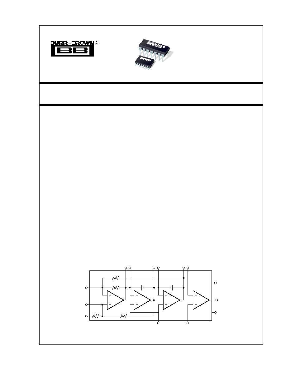
DESCRIPTION
The UAF42 is a universal active filter which can be
configured for a wide range of low-pass, high-pass,
and band-pass filters. It uses a classical state-variable
analog architecture with an inverting amplifier and
two integrators. The integrators include on-chip 1000pF
capacitors trimmed to 0.5%. This solves one of the
most difficult problems of active filter design--
obtaining tight tolerance, low-loss capacitors.
A DOS-compatible filter design program allows easy
implementation of many filter types such as
Butterworth, Bessel, and Chebyshev. A fourth, un-
committed FET-input op amp (identical to the other
three) can be used to form additional stages, or for
special filters such as band-reject and Inverse
Chebyshev.
The classical topology of the UAF42 forms a time-
continuous filter, free from the anomalies and switch-
ing noise associated with switched-capacitor filter
types.
The UAF42 is available in 14-pin plastic DIP and
SOL-16 surface-mount packages, specified for the ≠
25
∞
C to +85
∞
C temperature range.
UAF42
International Airport Industrial Park ∑ Mailing Address: PO Box 11400, Tucson, AZ 85734 ∑ Street Address: 6730 S. Tucson Blvd., Tucson, AZ 85706 ∑ Tel: (520) 746-1111 ∑ Twx: 910-952-1111
Internet: http://www.burr-brown.com/ ∑ FAXLine: (800) 548-6133 (US/Canada Only) ∑ Cable: BBRCORP ∑ Telex: 066-6491 ∑ FAX: (520) 889-1510 ∑ Immediate Product Info: (800) 548-6132
High-Pass
Out
R
R
R
1000pF
(1)
In
2
In
3
In
1
R
1000pF
(1)
Band-Pass
Out
Low-Pass
Out
GND
V+
V≠
NOTE: (1) ±0.5%
R = 50k
±0.5%
UAF42
UAF42
SBFS002
UAF42
2
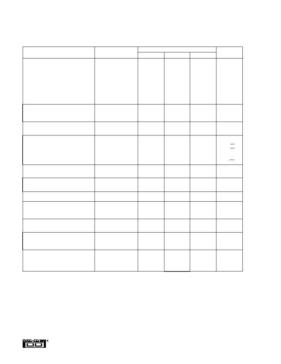
SPECIFICATIONS
ELECTRICAL
At T
A
= +25
∞
C, V
S
=
±
15V, unless otherwise noted.
UAF42AP, AU
PARAMETER
CONDITIONS
MIN
TYP
MAX
UNITS
FILTER PERFORMANCE
Frequency Range, fn
0 to 100
kHz
Frequency Accuracy
f = 1kHz
1
%
vs Temperature
0.01
%/
∞
C
Maximum Q
400
--
Maximun (Q ∑ Frequency) Product
500
kHz
Q vs Temperature
(f
O
∑ Q) < 10
4
0.01
%/
∞
C
(f
O
∑ Q) < 10
5
0.025
%/
∞
C
Q Repeatability
(f
O
∑ Q) < 10
5
2
%
Offset Voltage, Low-Pass Output
±
5
mV
Resistor Accuracy
0.5
1%
%
OFFSET VOLTAGE
(1)
Input Offset Voltage
±
0.5
±
5
mV
vs Temperature
±
3
µ
V/
∞
C
vs Power Supply
V
S
=
±
6 to
±
18V
80
96
dB
INPUT BIAS CURRENT
(1)
Input Bias Current
V
CM
= 0V
10
50
pA
Input Offset Current
V
CM
= 0V
5
pA
NOISE
Input Voltage Noise
Noise Density: f = 10Hz
25
nV/
Hz
f = 10kHz
10
nV/
Hz
Voltage Noise: BW = 0.1 to 10Hz
2
µ
Vp-p
Input Bias Current Noise
Noise Density: f = 10kHz
2
fA/
Hz
INPUT VOLTAGE RANGE
(1)
Common-Mode Input Range
±
11.5
V
Common-Mode Rejection
V
CM
=
±
10V
80
96
dB
INPUT IMPEDANCE
(1)
Differential
10
13
|| 2
|| pF
Common-Mode
10
13
|| 6
|| pF
OPEN-LOOP GAIN
(1)
Open-Loop Voltage Gain
V
O
=
±
10V, R
L
= 2k
90
126
dB
FREQUENCY RESPONSE
(1)
Slew Rate
10
V/
µ
s
Gain-Bandwidth Product
G = +1
4
MHz
Total Harmonic Distortion
G = +1, f = 1kHz
0.0004
%
OUTPUT
(1)
Voltage Output
R
L
= 2k
±
11
±
11.5
V
Short Circuit Current
±
25
mA
POWER SUPPLY
Specified Operating Voltage
±
15
V
Operating Voltage Range
±
6
±
18
V
Current
±
6
±
7
mA
TEMPERATURE RANGE
Specification
≠25
+85
∞
C
Operating
≠25
+85
∞
C
Storage
≠40
+125
∞
C
Thermal Resistance,
JA
100
∞
C/W
The information provided herein is believed to be reliable; however, BURR-BROWN assumes no responsibility for inaccuracies or omissions. BURR-BROWN assumes
no responsibility for the use of this information, and all use of such information shall be entirely at the user's own risk. Prices and specifications are subject to change
without notice. No patent rights or licenses to any of the circuits described herein are implied or granted to any third party. BURR-BROWN does not authorize or warrant
any BURR-BROWN product for use in life support devices and/or systems.
T
Same as specification for UAF42AP.
NOTES: (1) Specifications apply to uncommitted op amp, A
4
. The three op amps forming the filter are identical to A
4
but are tested as a complete filter.
3
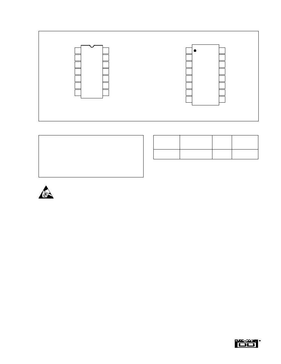
UAF42
1
2
3
4
5
6
7
8
16
15
14
13
12
11
10
9
Low-Pass V
O
NC
V
IN3
V
IN2
Auxiliary Op Amp, +In
Auxiliary Op Amp, ≠In
Auxiliary Op Amp, V
O
Bandpass V
O
Frequency Adj
2
NC
High-Pass V
O
V
IN1
Ground
V+
V≠
Frequency Adj
1
1
2
3
4
5
6
7
14
13
12
11
10
9
8
Low-Pass V
O
V
IN3
V
IN2
Auxiliary Op Amp, +In
Auxiliary Op Amp, ≠In
Auxiliary Op Amp, V
O
Bandpass V
O
Frequency Adj
2
High-Pass V
O
V
IN1
Ground
V+
V≠
Frequency Adj
1
Plastic DIP, P
U Package
SOL-16, 16-Pin SOIC
PIN CONFIGURATION
ABSOLUTE MAXIMUM RATINGS
Power Supply Voltage .......................................................................
±
18V
Input Voltage .............................................................................
±
V
S
±
0.7V
Output Short Circuit ................................................................. Continuous
Operating Temperature:
Plastic DIP, P; SOIC, U ................................................. ≠40
∞
C to +85
∞
C
Storage Temperature:
Plastic DIP, P; SOIC, U ............................................... ≠40
∞
C to +125
∞
C
Junction Temperature:
Plastic DIP, P; SOIC, U .............................................................. +125
∞
C
Lead Temperature (soldering, 10s) ................................................ +300
∞
C
Top View
NOTE: NC: No Connection. For best
performance connect all "NC" pins to
ground to minimize inter-lead capacitance.
PACKAGE
DRAWING
TEMPERATURE
PRODUCT
PACKAGE
NUMBER
(1)
RANGE
UAF42AP
Plastic 14-pin DIP
010
≠25
∞
C to +85
∞
C
UAF42AU
SOL-16
211
≠25
∞
C to +85
∞
C
NOTE: (1) For detailed drawing and dimension table, please see end of data
sheet, or Appendix C of Burr-Brown IC Data Book.
PACKAGE/ORDERING INFORMATION
ELECTROSTATIC
DISCHARGE SENSITIVITY
This integrated circuit can be damaged by ESD. Burr-Brown
recommends that all integrated circuits be handled with
appropriate precautions. Failure to observe proper handling
and installation procedures can cause damage.
ESD damage can range from subtle performance degradation
to complete device failure. Precision integrated circuits may
be more susceptible to damage because very small parametric
changes could cause the device not to meet its published
specifications.
UAF42
4
APPLICATIONS INFORMATION
The UAF42 is a monolithic implementation of the proven
state-variable analog filter topology. Pin-compatible with
the popular UAF41 Analog Filter, it provides several
improvements.
Slew Rate of the UAF42 has been increased to 10V/
µ
s
versus 1.6V/
µ
s for the UAF41. Frequency ∑ Q product of
the UAF42 has been improved, and the useful natural
frequency extended by a factor of four to 100kHz. FET-
input op amps on the UAF42 provide very low input bias
current. The monolithic construction of the UAF42 provides
lower cost and improved reliability.
DESIGN PROGRAM
Application Bulletin AB-035 and a computer-aided design
program, available from Burr-Brown, make it easy to design
and implement many kinds of active filters. The DOS-
compatible program guides you through the design process
and automatically calculates component values.
Low-pass, high-pass, band-pass and band-reject (notch)
filters can be designed. The program supports the three most
commonly used all-pole filter types: Butterworth, Chebyshev
and Bessel. The less-familiar Inverse Chebyshev is also
supported, providing a smooth passband response with ripple
in the stop-band.
With each data entry, the program automatically calculates
and displays filter performance. This allows a spreadsheet-
like "what if" design approach. For example, you can quickly
determine, by trial and error, how many poles are required
for a desired attenuation in the stopband. Gain/phase plots
may be viewed for any response type.
s
2
+ s
n
/Q +
n
2
A
LP
n
2
V
O
(s)
=
V
I
(s)
s
2
+ s
n
/Q +
n
2
A
HP
s
2
V
HP
(s)
=
V
I
(s)
s
2
+ s
n
/Q +
n
2
A
BP
(
n
/Q) s
V
BP
(s)
=
V
I
(s)
s
2
+ s
n
/Q +
n
2
A
BR
(s
2
+
n
2
)
V
BR
(s)
=
V
I
(s)
(1)
(2)
(3)
(4)
The basic building element of the most commonly used filter
types is the second-order section. This section provides a
complex-conjugate pair of poles. The natural frequency,
n
,
and Q of the pole pair determines the characteristic response
of the section. The low-pass transfer function is
The high-pass transfer function is
The band-pass transfer function is
A band-reject response is obtained by summing the low-pass
and high-pass outputs, yielding the transfer function
The most commonly used filter types are formed with one or
more cascaded second-order sections. Each section is de-
signed for
n
and Q according to the filter type (Butterworth,
Bessel, Chebyshev, etc.) and cutoff frequency. While tabu-
lated data can be found in virtually any filter design text, the
design program eliminates this tedious procedure.
Second-order sections may be non-inverting (Figure 1) or
inverting (Figure 2). Design equations for these two basic
configurations are shown for reference. The design program
solves these equations, providing complete results, includ-
ing component values.
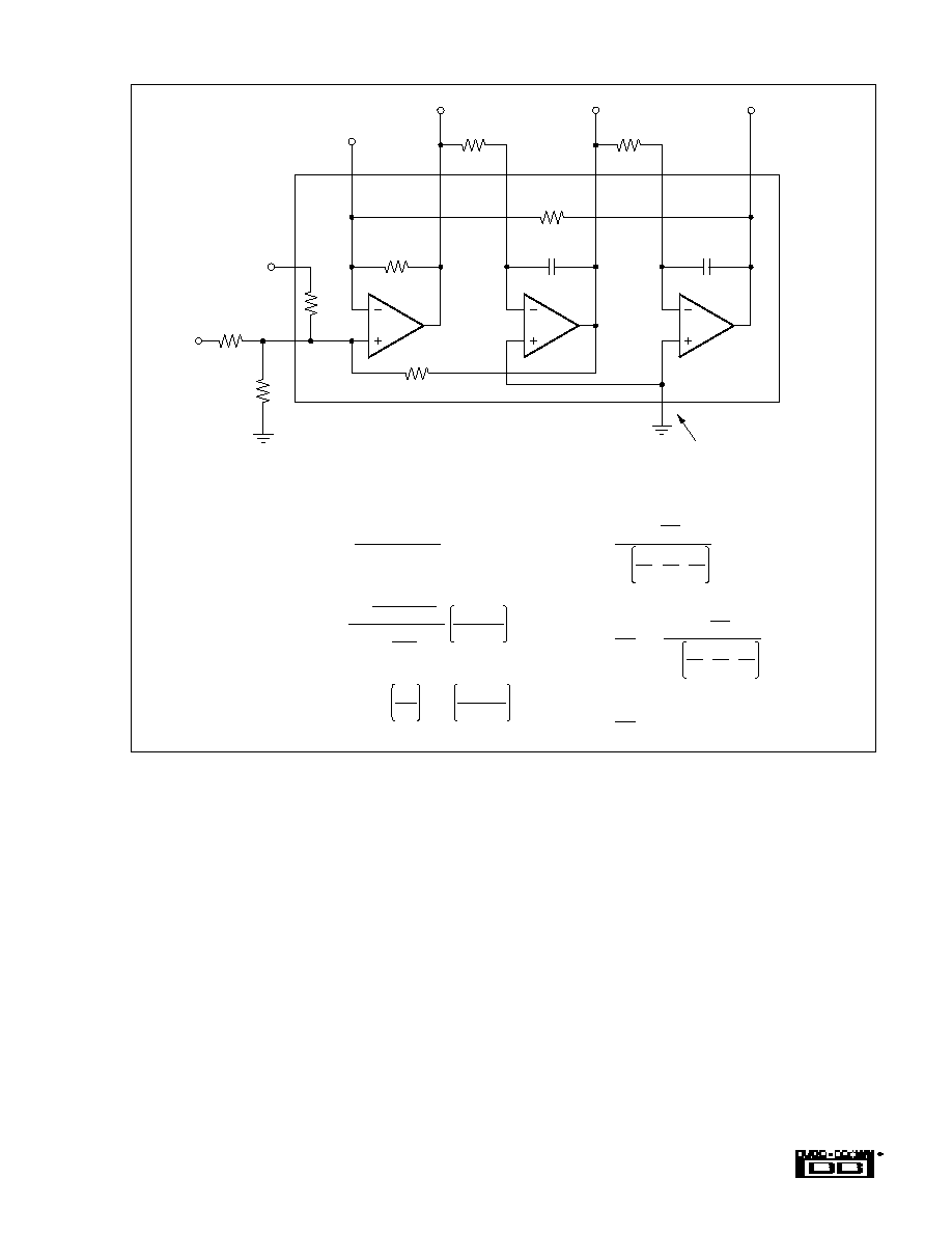
5
UAF42
FIGURE 1. Non-Inverting Pole-Pair.
A
1
R
2
50k
A
2
A
3
R
4
50k
UAF42
11
R1
50k
R
F1
R
F2
C
1
1000pF
C
2
1000pF
3
13
8
7
14
R
Q
LP Out
BP Out
HP Out
1
12
50k
R
G
V
IN
2
NOTE: If R
G
= 50k
, you can eliminate the external
gain-setting resistor by connecting V
IN
to pin 2.
Pin numbers are for DIP
package. SOL-16 pinout
is different.
R
G
R
Q
Design Equations
1.
n
2
=
R
2
R
1
R
F1
R
F2
C
1
C
2
2. Q
=
R
4
(R
G
+
R
Q
)
1 +
R
1
R
2
1 +
R
2
R
F1
C
1
R
1
R
F2
C
2
1/2
3. QA
LP
= QA
HP
R
1
R
F1
C
1
R
2
R
F2
C
2
1/2
R
1
R
2
= A
BP
R
2
4. A
LP
=
R
1
1 +
R
G
R
G
1
+
R
Q
1
+
R
4
1
R
1
5. A
HP
=
R
2
1 +
R
G
R
G
1
+
R
Q
1
+
R
4
1
R
1
R
2
A
LP
=
6. A
BP
=
R
G
R
4