 | –≠–ª–µ–∫—Ç—Ä–æ–Ω–Ω—ã–π –∫–æ–º–ø–æ–Ω–µ–Ω—Ç: UC1-2 | –°–∫–∞—á–∞—Ç—å:  PDF PDF  ZIP ZIP |
UC182-1,-2,-3,-ADJ
UC282-1,-2,-3,-ADJ
UC382-1,-2,-3,-ADJ
SLUS317 - JANUARY 1999
FEATURES
∑
Fast Transient Response
∑
10mA to 3A Load Current
∑
Short Circuit Protection
∑
Maximum Dropout of 450mV at 3A
Load Current
∑
Separate Bias and VIN Pins
∑
Available in Adjustable or Fixed
Output Voltages
∑
5 Pin Package allows Kelvin Sensing
of Load Voltage
∑
Reverse Current Protection
DESCRIPTION
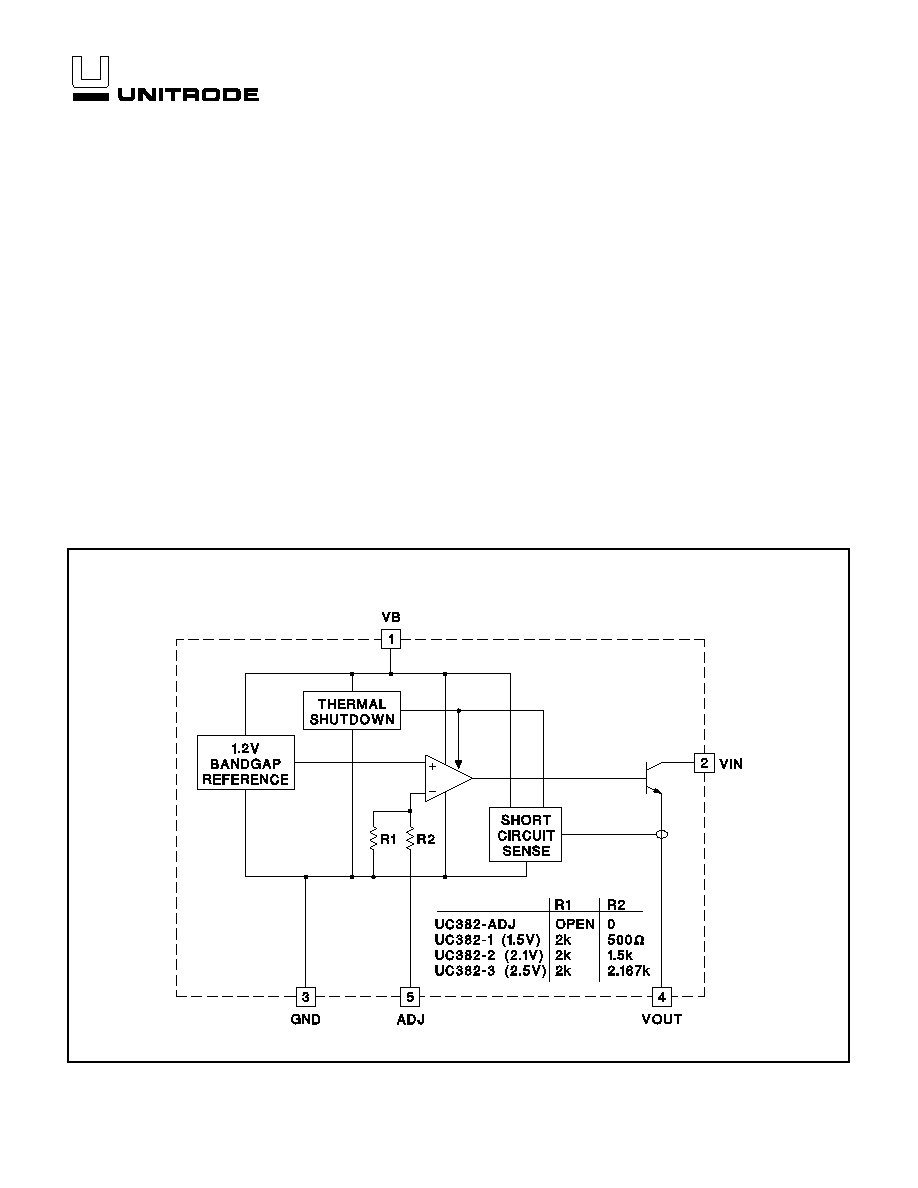
The UC382 is a low dropout linear regulator providing a quick response to
fast load changes. Combined with its precision on-board reference, the
UC382 excels at driving GTL and BTL buses. Due to its fast response to
load transients, the total capacitance required to decouple the regulator's
output can be significantly decreased when compared to standard LDO lin-
ear regulators.
Dropout voltage (VIN to VOUT) is only 450mV maximum at 100∞C and
350mV typical at 3A load.
The on-board bandgap reference is stable with temperature and scaled for
a 1.200V input to the internal power amplifier. The UC382 is available in
fixed output voltages of 1.5V, 2.1V, or 2.5V. The output voltage of the adjust-
able version can be set with two external resistors. If the external resistors
are omitted, the output voltage defaults to 1.2V.
Fast LDO Linear Regulator
BLOCK DIAGRAM
UDG-96037-1
2
UC182-1,-2,-3,-ADJ
UC282-1,-2,-3,-ADJ
UC382-1,-2,-3,-ADJ
ABSOLUTE MAXIMUM RATINGS
VB . . . . . . . . . . . . . . . . . . . . . . . . . . . . . . . . . . . . . . . . . . . . 13V
VIN . . . . . . . . . . . . . . . . . . . . . . . . . . . . . . . . . . . . . . . . . . +7.5V
Output Voltage . . . . . . . . . . . . . . . . . . . . . . . . . . . +1.2V to 6.0V
Storage Temperature . . . . . . . . . . . . . . . . . . . ≠65∞C to +150∞C
Junction Temperature . . . . . . . . . . . . . . . . . . . ≠55∞C to +150∞C
Lead Temperature (Soldering, 10 sec.) . . . . . . . . . . . . . +300∞C
Currents are positive into, negative out of the specified termi-
nal. Consult Packaging Section of Databook for thermal limita-
tions and considerations of packages.
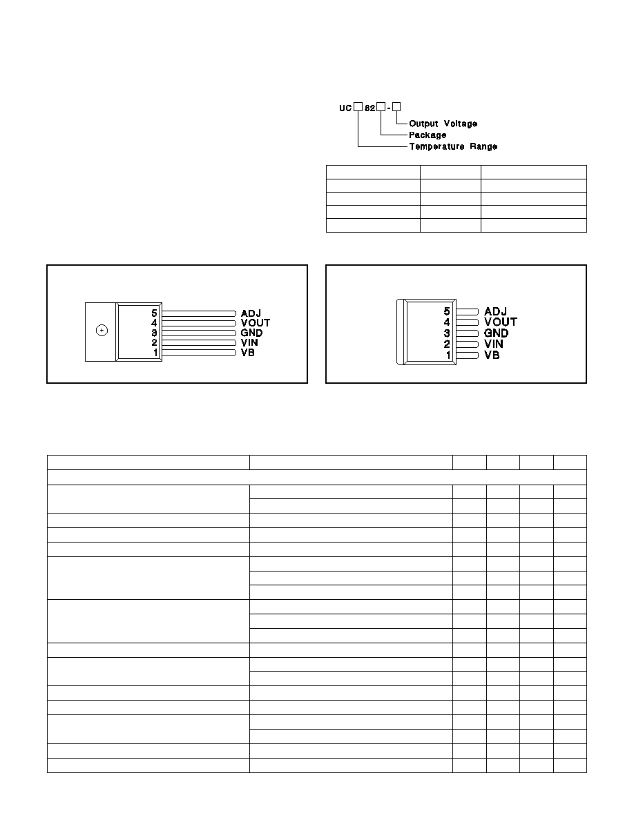
CONNECTION DIAGRAMS
5-Pin TO-220 (Top View)
T Package
5-Pin TO-263 (Top View)
TD Package
ORDERING INFORMATION
Temperature Range
Package
Output Voltage
1: ≠55∞C to +125∞C
T: TO-220
1: 1.5V
2: ≠25
∞
C to +100
∞
C
TD: TO-263
2: 2.1V
3: 0
∞
C to +100
∞
C
3: 2.5V
ADJ: 1.2V or Adjustable
Note: Tab tied to Pin 3.
Note: Tab tied to Pin 3.
ELECTRICAL CHARACTERISTICS:
Unless otherwise stated, these parameters apply for T
A
= ≠55
∞
C to 125∞C for the
UC182-X series, ≠25∞C to +100∞C for the UC282-X series and 0∞C to +100∞C for the UC382-X, VB = 5V; VIN = 3.3V, VOUT =
2.5V for the UC382-ADJ, T
A
= T
J
.
PARAMETERS
TEST CONDITIONS
MIN
TYP
MAX
UNITS
UC382-3 Fixed 2.5V, 3A Family
Output Voltage (I
VOUT
= 100mA)
UC382-3
2.475
2.500
2.525
V
UC282-3 and UC182-3
2.450
2.500
2.525
V
Load Regulation
I
VOUT
= 10mA to 3A
0.5
4
mV
VIN PSSR
80
100
dB
VB PSSR
50
60
dB
VIN Dropout Voltage = VIN≠VOUT
I
VOUT
= 3A, T
J
= 25∞C
350
425
mV
I
VOUT
= 3A, UC382-3
350
450
mV
I
VOUT
= 3A, UC282-3 and UC182-3
350
500
mV
VB Dropout = VB≠VOUT
I
VOUT
= 3A, UC382-3
1.8
2.10
V
I
VOUT
= 3A, UC282-3
1.8
2.20
V
I
VOUT
= 3A, UC182-3
1.8
2.35
V
Short Circuit Current Limit
3.3
4.5
A
VB Current
I
VOUT
= 10mA
6
9
mA
I
VOUT
= 3A
18
60
mA
VIN Current
I
VOUT
= 3A
2.94
2.97
A
UC382-2 Fixed 2.1V, 3A Family
Output Voltage (I
VOUT
= 100mA)
UC382-2
2.079
2.100
2.121
V
UC282-2 and UC182-2
2.058
2.100
2.121
V
Load Regulation
I
VOUT
= 10mA to 3A
0.5
4
mV
VIN PSSR
80
100
dB

3
UC182-1,-2,-3,-ADJ
UC282-1,-2,-3,-ADJ
UC382-1,-2,-3,-ADJ
ELECTRICAL CHARACTERISTICS:
Unless otherwise stated, these parameters apply for T
A
= ≠55
∞
C to 125∞C for the
UC182-X series, ≠25∞C to +100∞C for the UC282-X series and 0∞C to +100∞C for the UC382-X, VB = 5V; VIN = 3.3V, VOUT =
2.5V for the UC382-ADJ, T
A
= T
J
.
PARAMETERS
TEST CONDITIONS
MIN
TYP
MAX
UNITS
UC382-2 Fixed 2.1V, 3A Family (cont.)
VB PSSR
52
62
dB
VIN Dropout Voltage = VIN≠VOUT
I
VOUT
= 3A, T
J
= 25∞C
350
425
mV
I
VOUT
= 3A, UC382-2
350
450
mV
I
VOUT
= 3A, UC282-2 and UC182-2
350
500
mV
VB Dropout = VB≠VOUT
I
VOUT
= 3A, UC382-2
1.8
2.10
V
I
VOUT
= 3A, UC282-2
1.8
2.20
V
I
VOUT
= 3A, UC182-2
1.8
2.35
V
Short Circuit Current Limit
3.3
4.5
A
VB Current
I
VOUT
= 10mA
6
9
mA
I
VOUT
= 3A
18
60
mA
VIN Current
I
VOUT
= 3A
2.94
2.97
A
UC382-1 Fixed 1.5V, 3A Family
Output Voltage (I
VOUT
= 100mA)
UC382-1
1.485
1.500
1.515
V
UC282-1 and UC182-1
1.470
1.500
1.515
V
Load Regulation
I
VOUT
= 10mA to 3A
0.5
4
mV
VIN PSSR
80
100
dB
VB PSSR
55
65
dB
VIN Dropout Voltage = VIN≠VOUT
I
VOUT
= 3A, TJ = 25∞C
350
425
mV
I
VOUT
= 3A, UC282-1
350
450
mV
I
VOUT
= 3A, UC282-2 and UC182-1
350
500
mV
VB Dropout = VB≠VOUT
I
VOUT
= 3A, UC382-1
1.8
2.10
V
I
VOUT
= 3A, UC282-1
1.8
2.20
V
I
VOUT
= 3A, UC182-1
1.8
2.35
V
Short Circuit Current Limit
3.3
4.5
A
VB Current
I
VOUT
= 10mA
6
9
mA
I
VOUT
= 3A
18
60
mA
VIN Current
I
VOUT
= 3A
2.94
2.97
A
UC382-ADJ Adjustable, 3A Family
ADJ Voltage (I
VOUT
= 100 mA)
UC382-ADJ
1.188
1.200
1.212
V
UC282-ADJ and UC182-ADJ
1.176
1.200
1.212
V
Load Regulation
I
VOUT
= 10mA to 3A
0.5
4
mV
VIN PSSR
VOUT Programmed for 2.5V
80
100
dB
VB PSSR
VOUT Programmed for 2.5V
50
60
dB
VIN Dropout Voltage = VIN≠VOUT
I
VOUT
= 3A, T
J
= 25∞C
350
425
mV
I
VOUT
= 3A, UC382-ADJ
350
450
mV
I
VOUT
= 3A, UC282-ADJ and UC182-ADJ
350
500
mV
VB Dropout = VB≠VOUT
I
VOUT
= 3A, UC382-ADJ
1.8
2.10
V
I
VOUT
= 3A, UC282-ADJ
1.8
2.20
V
Short Circuit Current Limit
3.3
4.5
A
VB Current
I
VOUT
= 10mA
6
9
mA
I
VOUT
= 3A
18
60
mA
VIN Current
I
VOUT
= 3A
2.94
2.97
A
4
UC182-1,-2,-3,-ADJ
UC282-1,-2,-3,-ADJ
UC382-1,-2,-3,-ADJ
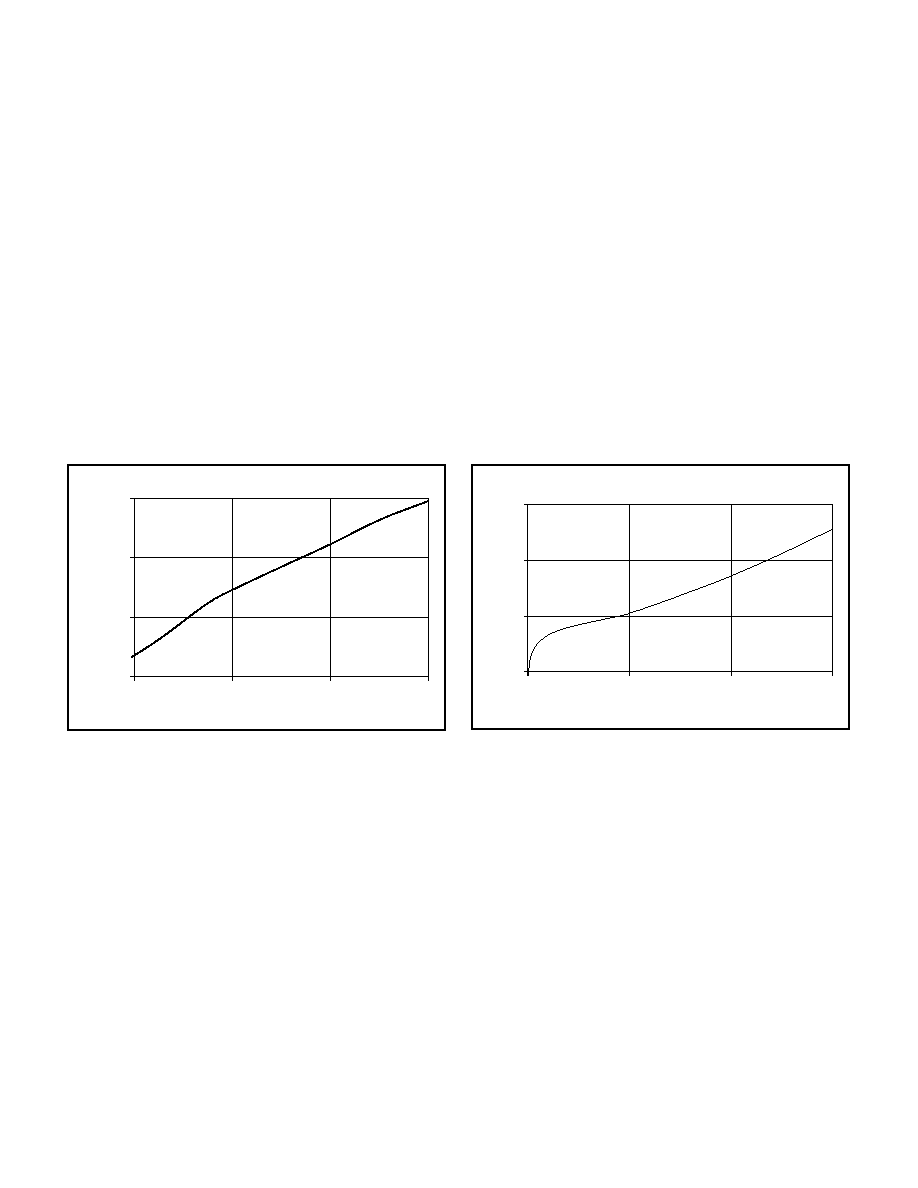
1.6
1.7
1.8
1.9
0
1
2
3
I
L
(A)
V
DR
OPOUT
(V)
Figure 1. Typical Dropout (V
B
- V
OUT
), T
J
= 27∞C
100
200
300
400
I
L
V
DRO
P
O
UT
(mV)
100mA
1A
2A
3A
Figure 2. Typical Dropout (V
IN
- V
OUT
), T
J
= 27∞C
PIN DESCRIPTIONS
ADJ: In the adjustable version, the user programs the
output voltage with two external resistors. The resistors
should be 0.1% for high accuracy. The output amplifier is
configured as a non-inverting operational amplifier. The
resistors should meet the criteria of R3 || R4 < 100
.
Connect ADJ to VOUT for an output voltage of 1.2V. Note
that the point at which the feedback network is
connected to the output is the Kelvin sense point.
GND: For accurate results, the GND pin should be
referenced to the load ground.
VB: Supplies power to all circuits of the regulator except
the collector of the output power transistor. The 2V
headroom from VB to VOUT allows the use of a
Darlington
output
stage
for
inherently
low
output
impedance and fast response. (Dropout is derated for
junction temperatures below 0∞C.)
VIN: Supplies the current to the collector of the output
power transistor only. The dropout (VIN-VOUT) is under
100mV for light loads; maximum dropout is 450mV at 3A
for T
J
= 0∞C to +110∞C. (Dropout is derated for junction
temperatures over 110∞C.) At full load, the majority of the
VB current is going to the load.
VOUT: This pin should be connected to the load via a
low impedance path. Avoid connectors which add
significant inductance and resistance. Note that even
though a Kelvin sense is available through a 5 pin
package, care must be taken since voltage drops along
wire traces add to the dropout voltage.
The UC382 is easy to use. The adjustable version re-
quires two 0.1% resistors to set the output voltage. The
fixed versions of the UC382 require no external resistors.
All versions of the UC382 require decoupling capacitors
on the input and output. In a typical application, VB and
VIN are driven from switching power supplies which may
have large filter capacitors at their outputs. If the UC382
is further than 12 inches from the power supply, it is rec-
ommended to add local decoupling as close as possible
to the linear regulator.
Decouple the output of the UC382 with at least 100
µ
F of
high quality tantalum or Sanyo OSCON capacitors close
to the VOUT pin for maximum stability. Many applications
involving ultra fast GTL or BTL applications require addi-
tional capacitance close to the load. The exact amount
will vary according to speed and magnitude of the load
transients and the tolerance allowed for transients on
VOUT. When specifying the decoupling capacitors, the
series resistance of the capacitor bank is an important
factor in its ability to filter load transients.
The UC382 allows for Kelvin sensing the voltage at the
load. This improves regulation performance and elimi-
nates the voltage drops due to wire trace resistance. This
voltage drop must be added to the headroom (VIN to
VOUT and VB to VOUT). The dropout of 450mV is mea-
sured at the pins and does not include additional drops
due to trace resistance. The minimum load current is
10mA.
Two or more UC382's may be used in parallel. While sta-
ble, this arrangement does degrade the transient re-
sponse.
APPLICATION INFORMATION
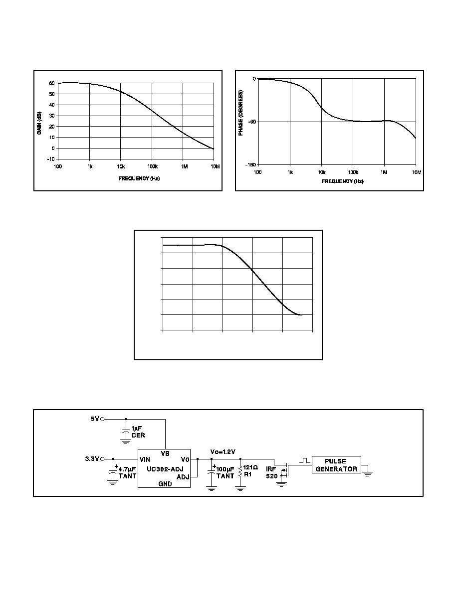
5
UC182-1,-2,-3,-ADJ
UC282-1,-2,-3,-ADJ
UC382-1,-2,-3,-ADJ
0
10
20
30
40
50
60
100
1k
10k
100k
1M
10M
FREQUENCY (Hz)
dB
Figure 5. PSRR (V
B
) 2.5V Out.
Figure 4. Open Loop Phase (100
µ
F Output
Capacitance, 1A Load).
Figure 3. Open Loop Gain (100
µ
F Output
Capacitance, 1A Load).
APPLICATION INFORMATION (cont.)
Figure 6. Transient test circuit.
UDG-96038