 | –≠–ª–µ–∫—Ç—Ä–æ–Ω–Ω—ã–π –∫–æ–º–ø–æ–Ω–µ–Ω—Ç: UC1517 | –°–∫–∞—á–∞—Ç—å:  PDF PDF  ZIP ZIP |
8/94
Stepper Motor Drive Circuit
UC1517
UC3517
ABSOLUTE MAXIMUM RATINGS
Second Level Supply, V
SS
. . . . . . . . . . . . . . . . . . . . . . . . . . 40V
Phase Output Supply, V
MM
. . . . . . . . . . . . . . . . . . . . . . . . . 40V
Logic Supply, V
CC
. . . . . . . . . . . . . . . . . . . . . . . . . . . . . . . . . . 7V
Logic Input Voltage . . . . . . . . . . . . . . . . . . . . . . . . . -.3V to +7V
Logic Input Current . . . . . . . . . . . . . . . . . . . . . . . . . . . . .
±
10mA
Output Current, Each Phase . . . . . . . . . . . . . . . . . . . . . . 500mA
Output Current, Emitter Follower . . . . . . . . . . . . . . . . . . -500mA
Power Dissipation, (Note). . . . . . . . . . . . . . . . . . . . . . . . . . . . 1W
Power Dissipation, (Note) . . . . . . . . . . . . . . . . . . . . . . . . . . . 2W
Junction Temperature . . . . . . . . . . . . . . . . . . . . . . . . . . . . 150∞C
Ambient Temperature, UC1517 . . . . . . . . . . . . -55∞C to +125∞C
Ambient Temperature, UC3517 . . . . . . . . . . . . . . 0∞C to +70∞C
Storage Temperature . . . . . . . . . . . . . . . . . . . -55∞C to +150∞C
Note: Consult Packaging section of Databook for thermal
limitations and considerations of package.
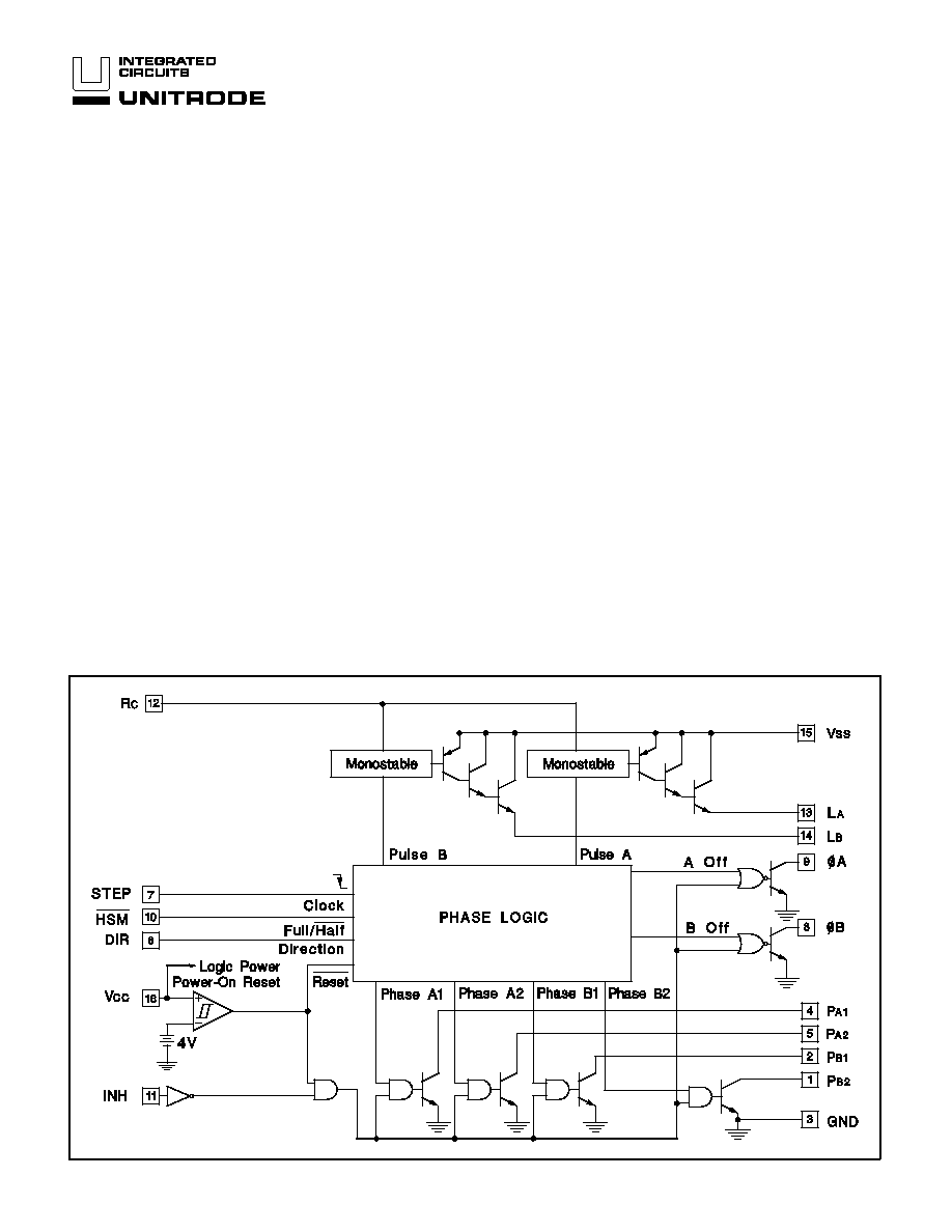
BLOCK DIAGRAM
FEATURES
∑
Complete Motor Driver and Encoder
∑
Continuous Drive Capability 350mA per Phase
∑
Contains all Required Logic for Full and Half
Stepping
∑
Bilevel Operation for Fast Step Rates
∑
Operates as a Voltage Doubler
∑
Useable as a Phase Generator and/or as a
Driver
∑
Power-On Reset Guarantees Safe,
Predictable Power-Up
DESCRIPTION
The UC3517 contains four NPN drivers that operate in two-phase
fashion for full-step and half-step motor control. The UC3517
also contains two emitter followers, two monostables, phase de-
coder logic, power-on reset, and low-voltage protection, making it
a versatile system for driving small stepper motors or for control-
ling large power devices.
The emitter followers and monostables in the UC3517 are config-
ured to apply higher-voltage pulses to the motor at each step
command. This drive technique, called "Bilevel," allows faster
stepping than common resistive current limiting, yet generates
less electrical noise than chopping techniques.

PARAMETER
TEST CONDITIONS
UC1517 / UC3517
UNITS
MIN
TYP
MAX
Logic Supply, V
CC
Pin 16
4.75
5.25
V
Second Supply, V
SS
Pin 15
10
40
V
Logic Supply Current
V
INH
= 0.4V
45
60
mA
V
INH
= 4.0V
12
mA
Input Low Voltage
Pins 6, 7, 10, 11
0.8
V
Input High Voltage
Pins 6, 7, 10, 11
2.0
V
Input Low Current
Pins 6, 7, 10, 11; V = 0V
-400
µ
A
Input High Current
Pins 6, 7, 10, 11; V = 5V
20
µ
A
Phase Output Saturation Voltage
Pins 1, 2, 4, 5; I = 350mA
0.6
0.85
V
Phase Output Leakage Current
Pins 1, 2, 4, 5; V = 39V
500
µ
A
Follower Saturation Voltage to V
SS
Pins 13,14; I = 350mA
-2
V
Follower Leakage Current
Pins 13,14; V = 0V
500
µ
A
Output Low Voltage, ÿ
A
, ÿ
B
Pins 8, 9; I = 1.6mA
0.1
0.4
V
Phase Turn-On Time
Pins 1, 2, 4, 5
2
µ
s
Phase Turn-Off Time
Pins 1, 2, 4, 5
1.8
µ
s
Second-Level On Time. T
MONO
Pins 13,14; Figure 3 Test Circuit
275
325
375
µ
s
Logic Input Set-up Time, t
S
Pins 6, 10; Figure 4
400
ns
Logic Input Hold Time, t
h
Pins 6, 10; Figure 4
0
ns
STEP Pulse Width, t
P
Pin 7; Figure 4
800
ns
Timing Resistor Value
Pin 12
1k
100k
Timing Capacitor Value
Pin 12
0.1
500
nF
Power-On Threshold
Pin 16
4.3
V
Power-Off Threshold
Pin 16
3.8
V
Power Hysteresis
Pin 16
0.5
V
UC1517
UC3517
PACKAGE PIN FUNCTION
FUNCTION
PIN
N/C
1
P
B2
2
P
B1
3
GND
4
P
A1
5
N/C
6
P
A2
7
DIR
8
STEP
9
ÿ
B
10
N/C
11
ÿ
A
12
HSM
13
INH
14
RC
15
N/C
16
L
A
17
L
B
18
V
SS
19
V
CC
20
PLCC-20, LCC-20
(TOP VIEW)
Q & L PACKAGE
DIL-16 (TOP VIEW)
J or N Package
CONNECTION DIAGRAMS
Unless otherwise stated, these specifications apply for T
A
= -55∞C to +125∞C for the
UC1517 and 0∞C to +70∞C for the UC3517, Vcc=5V, V
SS
= 20V, T
A
=T
J.
Pin
numbers refer to DIL-16 package.
ELECTRICAL CHARACTERISTICS:
2
PIN DESCRIPTION
V
CC:
V
CC
is the UC3517's logic supply. Connect to a
regulated 5VDC, and bypass with a 0.1
µ
F ceramic ca-
pacitor to absorb switching transients.
V
MM
: V
MM
is the primary motor supply. It connects to the
UC3517 phase outputs through the motor windings. Limit
this supply to less than 40V to prevent breakdown of the
phase output transistors. Select the nominal V
MM
voltage
for the desired continuous winding current.
V
SS
: V
SS
is the secondary motor supply. It drives the L
A
and L
B
outputs of the UC3517 when a monostable in the
UC3517 is active. In the bilevel application, this supply is
applied to the motor to charge the winding inductance
faster than the primary supply could. Typically, Vss is
higher in voltage than V
MM
, although V
SS
must be less
than 40V. The V
SS
supply should have good transient ca-
pability.
GROUND: The ground pin is the common reference for
all supplies, inputs and outputs.
RC: RC controls the timing functions of the monostables
in the UC3517. It is normally connected to a resistor (R
T
)
and a capacitor (C
T
) to ground, as shown in Figure 3.
Monostable on time is determined by the formula T
ON
0.69 R
T
C
T
. To keep the monostable on indefinitely, pull
RC to V
CC
through a 50k resistor. The UC3517 contains
only one RC pin for two monostables. If step rates com-
parable to T
ON
are commanded, incorrect pulsing can re-
sult, so consider maximum step rates when selecting R
T
and C
T.
Keep T
ON
T
STEP MAX
.
ÿ
A
and ÿ
B
: These logic outputs indicate half-step posi-
tion. These outputs are open-collector, low-current driv-
ers, and may directly drive TTL logic. They can also drive
CMOS logic if a pull-up resistor is provided. Systems
which use the UC3517 as an encoder and use a different
driver can use these outputs to disable the external driver,
as shown in Figure 8. The sequencing of these outputs is
shown in Figure 5.
P
A1
, P
A2
, P
B1
, and P
B2
: The phase outputs pull to
ground sequentially to cause motor stepping, according to
the state diagram of Figure 5. The sequence of stepping
on these lines, as well as with the L
A
and L
B
lines is con-
trolled by STEP input, the DIR input, and the HSM input.
Caution: If these outputs or any other IC pins are pulled
too far below ground either continuously or in a transient,
step memory can be lost. It is recommended that these
pins be clamped to ground and supply with high-speed di-
odes when driving inductive loads such as motor wind-
ings or solenoids. This clamping is very important
because one side of the winding can "kick" in a direction
opposite the swing of the other side.
L
A
and L
B
: These outputs pull to V
SS
when their corre-
sponding monostable is active, and will remain high until
the monostable time elapses. Before and after, these out-
puts are high-impedance. For detail timing information,
consult Figure 5.
STEP: This logic input clocks the logic in the UC3517 on
every falling edge. Like all other UC3517 inputs, this input
is TTL/CMOS compatible, and should not be pulled below
ground.
DIR: This logic input controls the motor rotation direction
by controlling the phase output sequence as shown in
Figure 5. This signal must be stable 400ns before a falling
edge on STEP, and must remain stable through the edge
to insure correct stepping.
HSM: This logic input switches the UC3517 between half-
stepping (HSM = low) and full-stepping (HSM = high) by
controlling the phase output sequence as show in Figure
5. This line requires the same set-up time as the DIR in-
put, and has the same hold requirement.
UC1517
UC3517
Figure 3.
Test Circuit
Figure 4.
Timing Waveforms
3

UC1517
UC3517
INH: When the inhibit input is high, the phase and
out-
puts are inhibited (high impedance). STEP pulses re-
ceived while inhibited will continue to update logic in the
IC, but the states will not be reflected at the outputs until
inhibit is pulled low. In stepper motor systems, this can be
used to save power or to allow the rotor to move freely for
manual repositioning.
OPERATING MODES
The UC3517 is a system component capable of many dif-
ferent operating modes, including:
Unipolar Stepper Driver: In its simplest form, the
UC3517 can be connected to a stepper motor as a unipo-
lar driver. L
A
, L
B
, RC and Vss are not used, and may be
left open. All other system design considerations men-
tioned above apply, including choice of motor supply
VMM, undershoot diodes and timing considerations.
Unipolar Bilevel Stepper Driver: If increased step rates
are desired, the application circuit of Figure 6 makes use
of the monostables and emitter followers as well as the
configuration mentioned above to provide high-voltage
pulses to the motor windings when the phase is turned
on. For a given dissipation level, this mode offers faster
step rates, and very little additional electrical noise.
The choice of monostable components can be estimated
based on the timing relationship of motor current and volt-
age: V = Ldl/dt. Assuming a fixed secondary supply volt-
age (V
SS
), a fixed winding inductance (L
M
), a desired
winding peak current (I
W
), and no back EMF from the mo-
tor, we can estimate that R
T
C
T
= 1.449 I
W
L
M
/V
SS
. In
practice, these calculations should be confirmed and ad-
justed to accommodate for effects not modeled.
Voltage-Doubled Mode: The UC3517 can also be used
to generate higher voltages than available with the sys-
tem power supplies using capacitors and diodes. Figure 9
shows how this might be done, and gives some estimates
for the component values.
Higher Current Operation: For systems requiring more
than 350mA of drive per phase, the UC3717A can be
used in conjunction with discrete power transistors or
power driver ICs, like the L298. These can be connected
as current gain devices that turn on when the phase out-
puts turn on.
Bipolar Motor Drive: Bipolar motors can be controlled by
the UC3517 with the addition of bipolar integrated drivers
such as the UC3717A (Figure 8) and the L298, or discrete
devices. Care should be taken with discrete devices to
avoid potential cross-conduction problems.
LOGIC FLOW GRAPH
The UC3517 contains a bidirectional counter which is de-
coded to generate the correct phase and ÿ outputs. This
counter is incremented on every falling edge of the STEP
input. Figure 5 shows a graph representing the counter
sequence, inputs that determine the next state (DIR and
HSM), and the outputs at each state. Each circle repre-
sents a unique logic state, and the four inside circles rep-
resent the half-step states.
The four bits inside the circles represent the phase out-
puts in each state (P
A1
, P
A2
, P
B1
, and P
B2
). For example,
the circle labeled 1010 is immediately entered when the
device is powered up, and represents P
A1
off ("1" or
high), P
A2
on ("0" or low), P
B1
off ("1" or high) and P
B2
on
("0" or low). The ÿ
A
and ÿ
B
outputs are both low (uniden-
tified).
The arrows in the graph show the state changes. For ex-
ample, if the IC is in state 0110, DIR is high, HSM is high,
and STEP falls, the next state will be 0101, and a pulse
will be generated on the L
B
line by the monostable.
Inhibit will not effect the logic state, but it will cause all
phase outputs and both
ÿ outputs to go high (off). A fall-
ing edge on STEP will still cause a state change, but in-
hibit will have to toggle low for the state to be apparent.
A falling edge on STEP with HSM high will cause the
counter to advance to the next full step state regardless
of whether or not it was in a full step state previously.
No L
A
or L
B
pulses are generated entering half-states.
4

UC1517
UC3517
For applications requiring very fast step rates, a zener diode
permits windings to discharge at higher voltages, and higher
rates. Driver transistor breakdown must be considered when
selecting Vss and zener voltage to insure that the outputs will
not overshoot past 40V. If the zener diodes are not used and
UC3610 pin 2 is connected directly to Vss then higher Vss can
be used.
Figure 6.
Bilevel Motor Driver
Figure 5.
Logic Flow Graph
5