
UC1524A
UC2524A
UC3524A
DESCRIPTION
The UC1524A family of regulating PWM ICs has been designed to retain the
same highly versatile architecture of the industry standard UC1524 (SG1524)
while offering substantial improvements to many of its limitations. The UC1524A
is pin compatible with "non-A" models and in most existing applications can be
directly interchanged with no effect on power supply performance. Using the
UC1524A, however, frees the designer from many concerns which typically had
required additional circuitry to solve.
The UC1524A includes a precise 5V reference trimmed to
±
1% accuracy, elimi-
nating the need for potentiometer adjustments; an error amplifier with an input
range which includes 5V, eliminating the need for a reference divider; a current
sense amplifier useful in either the ground or power supply output lines; and a
pair of 60V, 200mA uncommitted transistor switches which greatly enhance out-
put versatility.
An additional feature of the UC1524A is an under-voltage lockout circuit which
disables all the internal circuitry, except the reference, until the input voltage has
risen to 8V. This holds standby current low until turn-on, greatly simplifying the
design of low power, off-line supplies. The turn-on circuit has approximately
600mV of hysteresis for jitter-free activation.
Other product enhancements included in the UC1524A's design include a PWM
latch which insures freedom from multiple pulsing within a period, even in noisy
environments, logic to eliminate double pulsing on a single output, a 200ns ex-
ternal shutdown capability, and automatic thermal protection from excessive
chip temperature. The oscillator circuit of the UC1524A is usable beyond 500kHz
and is now easier to synchronize with an external clock pulse.
The UC1524A is packaged in a hermetic 16-pin DIP and is rated for operation
from -55∞C to +125∞C. The UC2524A and 3524A are available in either ceramic
or plastic packages and are rated for operation from -40∞C to +85∞C and 0∞C to
70∞C, respectively. Surface mount devices are also available.
FEATURES
∑
Fully Interchangeable with
Standard UC1524 Family
∑
Precision Reference Internally
Trimmed to
±
1%
∑
High-Performance Current Limit
Function
∑
Under-Voltage Lockout with
Hysteretic Turn-on
∑
Start-Up Supply Current Less
Than 4mA
∑
Output Current to 200mA
∑
60V Output Capability
∑
Wide Common-Mode Input
Range for both Error and
Current Limit Amplifiers
∑
PWM Latch Insures Single
Pulse per Period
∑
Double Pulse Suppression
Logic
∑
200ns Shutdown through PWM
Latch
∑
Guaranteed Frequency
Accuracy
∑
Thermal Shutdown Protection
Advanced Regulating Pulse Width Modulators
15
3
6
7
9
1
2
4
5
16
12
11
13
14
10
8
+
≠
+
+
≠
V
IN
V
IN
+
≠
OSC
6V
CL (≠) SENSE
N.I. INPUT
COMP
C
T
R
T
OSC
V
IN
CL (+) SENSE
INV. INPUT
U.V.
SENSE
POWER TO
INTERNAL
CIRCUITRY
+5V
REFERENCE
REGULATOR
V
REF
C
A
E
A
C
B
E
B
SHUTDOWN
GND
PWM
LATCH
FLIP
FLOP
10k
1k
5.5V
C/L
E/A
200mV
RAMP
COMP
CLOCK
E/A
S
S
R
T
BLOCK DIAGRAM
SLUS181A - NOVEMBER 1999
UDG-99178

2
UC1524A
UC2524A
UC3524A
ABSOLUTE MAXIMUM RATINGS
Supply Voltage (V
IN
) . . . . . . . . . . . . . . . . . . . . . . . . . . . . . . 40V
Collector Supply Voltage (V
C
) . . . . . . . . . . . . . . . . . . . . . . . 60V
Output Current (each Output) . . . . . . . . . . . . . . . . . . . . . 200mA
Maximum Forced Voltage (Pin 9, 10) . . . . . . . . . . . . . -3 to +5V
Maximum Forced Current (Pin 9, 10) . . . . . . . . . . . . . . .
±
10mA
Reference Output Current . . . . . . . . . . . . . . . . . . . . . . . . 50mA
Oscillator Charging Current . . . . . . . . . . . . . . . . . . . . . . . . 5mA
Power Dissipation at T
A
= +25∞C. . . . . . . . . . . . . . . . . 1000mW
Power Dissipation at T
C
= +25∞C . . . . . . . . . . . . . . . . 2000mW
Operating Temperature Range . . . . . . . . . . . . -55∞C to +125∞C
Storage Temperature Range . . . . . . . . . . . . . . -65∞C to +150∞C
Lead Temperature, (Soldering, 10 seconds) . . . . . . . . . +300∞C
Note: Consult packaging section of Databook for thermal limita-
tions and considerations of package.
CONNECTION DIAGRAMS
DIL-16, SOIC-16 (TOP VIEW)
J or N Package, DW Package
PACKAGE PIN FUNCTION
FUNCTION
PIN
N/C
1
Inv. Input
2
Non-Inv. Input
3
OSC/SYNC
4
C.L. (+) sense
5
N/C
6
C.L. (-) sense
7
R
T
8
C
T
9
Ground
10
N/C
11
Compensation
12
Shutdown
13
Emitter A
14
Collector A
15
N/C
16
Collector B
17
Emitter B
18
+V
IN
19
+5V V
REF
20
PLCC-20, LCC-20 (TOP VIEW)
Q or L Package
PARAMETER
TEST CONDITIONS
UC1524A / UC2524A
UC3524A
UNITS
MIN
TYP
MAX
MIN
TYP
MAX
Turn-on Characteristics
Input Voltage
Operating Range after Turn-on
8
40
8
40
V
Turn-on Threshold
6.5
7.5
8.5
6.5
7.5
8.5
V
Turn-on Current
V
IN
= 6V
2.5
4
2.5
4
mA
Operating Current
V
IN
= 8 to 40V
5
10
5
10
mA
Turn-on Hysteresis*
0.5
0.5
V
Reference Section
Output Voltage
T
J
= 25∞C
4.95
5.00
5.05
4.90
5.00
5.10
V
Over Operating Range
4.9
5.1
4.85
5.15
V
Line Regulation
V
IN
= 10 to 40V
10
20
10
30
mV
Load Regulation
I
L
= 0 to 20 mA
20
25
20
35
mV
Temperature Stability*
Over Operating Range*
20
25
20
35
mV
Short Circuit Current
V
REF
= 0, 25∞C
T
J
125∞C
80
100
80
100
mA
Output Noise Voltage*
10Hz
f
10kHz, T
J
=25∞C
40
40
µ
Vrms
Long Term Stability*
T
J
=125∞C, 1000 Hrs.
20
50
20
50
mV
ELECTRICAL CHARACTERISTICS:
Unless otherwise stated, these specifications apply for T
A
= -55∞C to +125∞C for the
UC1524A, -40∞ to +85∞C for the UC2524A, and 0∞C to + 70∞C for the UC3524A; V
IN
= V
C
= 20V, T
A
= T
J.
* These parameters are ensured by design but not 100% tested in production.

3
UC1524A
UC2524A
UC3524A
PARAMETER
TEST CONDITIONS
UC1524A / UC2524A
UC3524A
UNITS
MIN
TYP
MAX
MIN
TYP
MAX
Oscillator Section (Unless otherwise specified, R
T
= 2700
, C
T
= 0.01 mfd)
Initial Accuracy
T
J
= 25∞C
41
43
45
39
43
47
kHz
Over Operating Range
40.2
45.9
38.2
47.9
kHz
Temperature Stability*
Over Operating Temperature Range
1
2
1
2
%
Minimum Frequency
R
T
= 150k
, C
T
= 0.1mfd
140
120
Hz
Maximum Frequency
R
T
= 2.0k
, C
T
= 470pF
500
500
kHz
Output Amplitude*
3
3.5
3
3.5
V
Output Pulse Width*
0.29
0.5
1.0
0.3
0.5
1.0
µ
s
Ramp Peak
3.3
3.5
3.7
3.3
3.5
3.7
V
Ramp Valley
T
J
= 25∞C
0.7
0.8
0.9
0.7
0.8
0.9
V
Ramp Valley T.C.
-1.0
-1.0
mV/∞C
Error Amplifier Section (Unless otherwise specified, V
CM
= 2.5V)
Input Offset Voltage
0.5
5
2
10
mV
Input Bias Current
1
5
1
10
µ
A
Input Offset Current
.05
1
0.5
1
µ
A
Common Mode Rejection Ratio V
CM
= 1.5 to 5.5V
70
80
70
80
dB
Power Supply Rejection Ratio
V
IN
= 10 to 40V
70
80
70
80
dB
Output Swing (Note 1)
5.0
0.5
5.0
0.5
V
Open Loop Voltage Gain
V
O= 1 to 4V, RL
10M
72
80
64
80
dB
Gain-Bandwidth*
T
J
= 25∞C, A
V
= 0dB
1
3
1
3
MHz
DC Transconductance*ß
T
J
= 25∞C, 30k
R
L
1M
1.7
2.3
1.7
2.3
mS
P.W.M. Comparator (R
T
= 2k
, C
T
= 0.01mfd)
Minimum Duty Cycle
V
COMP
= 0.5V
0
0
%
Maximum Duty Cycle
V
COMP
= 3.8V
45
45
%
Current Limit Amplifier (Unless otherwise specified, Pin 5 = 0V)
Input Offset Voltage
T
J
= 25∞C, E/A Set for Maximum
Output
190
200
210
180
200
220
mV
Over Operating Temperature Range
180
220
170
230
mV
Input Bias Current
-1
-10
-1
-10
µ
A
Common Mode Rejection Ratio V
(pin 5)
= -0.3V to + 5.5V
50
60
50
60
dB
Power Supply Rejection Ratio
V
IN
= 10 to 40V
50
60
50
60
dB
Output Swing (Note 1)
Minimum Total Range
5.0
0.5
5.0
0.5
V
Open-Loop Voltage Gain
V
O
= 1 to 4V, R
L
10M
70
80
70
80
dB
Delay Time*
Pin 4 to Pin 9,
V
IN
= 300mV
300
300
ns
Output Section (Each Output)
Collector Emitter Voltage
I
C
= 100
µ
A
60
80
60
80
V
Collector Leakage Current
V
CE
= 50V
.1
20
.1
20
µ
A
ELECTRICAL CHARACTERISTICS:
Unless otherwise stated, these specifications apply for T
A
= -55∞C to +125∞C for the
UC1524A, -40∞ to +85∞C for the UC2524A, and 0∞C to + 70∞C for the UC3524A; V
IN
= V
C
= 20V, T
A
= T
J.
* These parameters are ensured by design but not 100% tested in production.
ß DC transconductance (g
M
) relates to DC open-loop voltage gain according to the following equation: A
V
= g
M
R
L
where R
L
is the resistance from pin 9 to the common mode voltage.
The minimum g
M
specification is used to calculate minimum A
V
when the error amplifier output is loaded.
Note 1: Min Limit applies to output high level, max limit applies to output low level.

4
UC1524A
UC2524A
UC3524A
PARAMETER
TEST CONDITIONS
UC1524A / UC2524A
UC3524A
UNITS
MIN
TYP
MAX
MIN
TYP
MAX
Output Section ( cont.) (Each Output)
Saturation Voltage
I
C
= 20mA
I
C
= 200mA
.2
1
.4
2.2
.2
1
.4
2.2
V
V
Emitter Output Voltage
I
E
= 50mA
17
18
17
18
V
Rise Time*
T
J =
25∞C, R = 2k
120
400
120
400
ns
Fall Time*
T
J
= 25∞C, R = 2k
25
200
25
200
ns
Comparator Delay*
T
J
= 25∞C, Pin 9 to output
300
300
ns
Shutdown Delay*
T
J
= 25∞C, Pin 10 to output
200
200
ns
Shutdown Threshold
T
J
= 25∞C, R
C
= 2k
0.6
.7
1.0
0.6
.7
1.0
V
S/D Threshold Over Temp.
Over Operating Temperature Range
0.4
1.2
0.4
1.0
V
Thermal Shutdown*
165
165
∞C
ELECTRICAL CHARACTERISTICS:
Unless otherwise stated, these specifications apply for T
A
= -55∞C to +125∞C for the
UC1524A, -40∞ to +85∞C for the UC2524A, and 0∞C to + 70∞C for the UC3524A; V
IN
= V
C
= 20V. T
A
= T
J.
* These parameters are ensured by design but not 100% tested in production.
OPEN-LOOP CIRCUIT
5
UC1524A
UC2524A
UC3524A
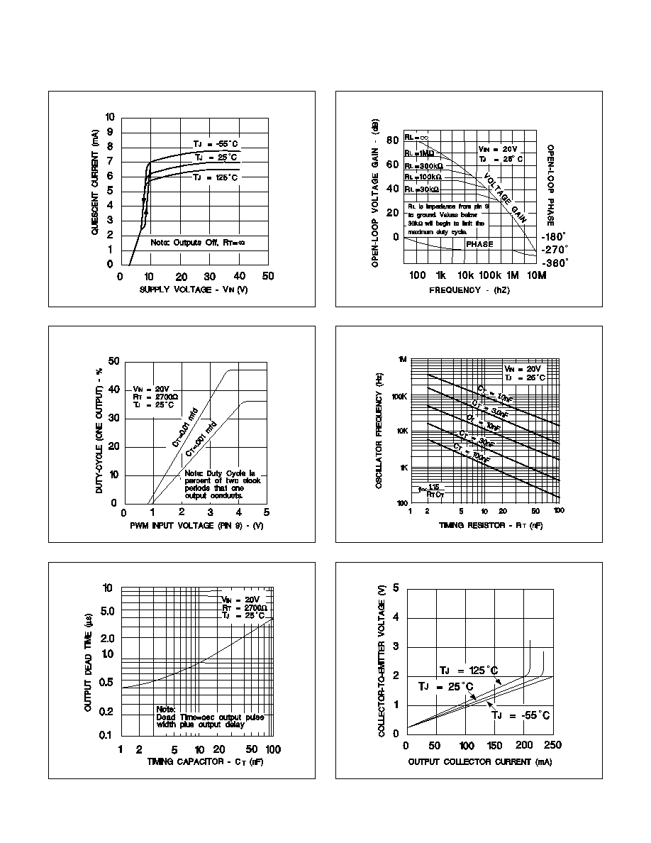
Output Dead Time vs Timing Capacitor Value
Pulse Width Modulator
Transfer Function
Output Saturation Voltage
Oscillator Frequency
vs Timing Components
Supply Current vs Voltage
Error Amplifier Voltage Gain
and Phase vs Frequency