 | –≠–ª–µ–∫—Ç—Ä–æ–Ω–Ω—ã–π –∫–æ–º–ø–æ–Ω–µ–Ω—Ç: UC1525AL | –°–∫–∞—á–∞—Ç—å:  PDF PDF  ZIP ZIP |
UC1525A/27A
UC2525A/27A
UC3525A/27A
Regulating Pulse Width Modulators
FEATURES
∑
8 to 35V Operation
∑
5.1V Reference Trimmed to
±
1%
∑
100Hz to 500kHz Oscillator Range
∑
Separate Oscillator Sync Terminal
∑
Adjustable Deadtime Control
∑
Internal Soft-Start
∑
Pulse-by-Pulse Shutdown
∑
Input Undervoltage Lockout with
Hysteresis
∑
Latching PWM to Prevent Multiple
Pulses
∑
Dual Source/Sink Output Drivers
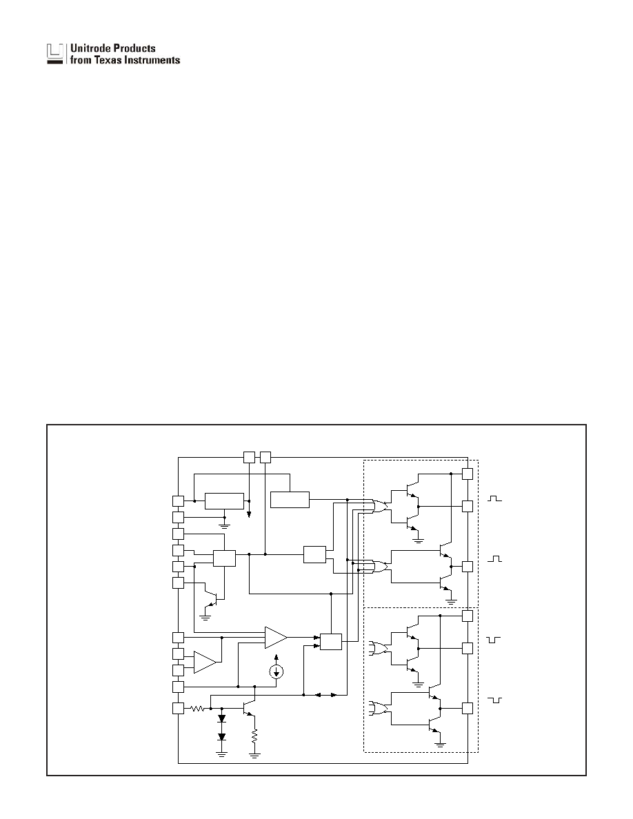
15
12
3
6
5
7
9
1
2
8
10
Reference
Regulator
16
UVLO
Lockout
4
OSC
3 k
5 k
50 µA
PWM
Latch
Flip
Flop
13
14
11
13
11
14
UC1527A Output Stage
UC1525A Output Stage
COMP
S
S
R
+VIN
GROUND
SYNC
RT
CT
DISCHARGE
COMPENSATION
INV INPUT
NI INPUT
SOFTSTART
SHUTDOWN
OUTPUT B
OUTPUT A
VC
OUTPUT B
OUTPUT A
VC
NOR
NOR
OR
OR
V
REF
Error
Amp
VREF
OSC
OUT
To internal
circuitry
BLOCK DIAGRAM
SLUS191B - February 1997 - Revised June 2005
DESCRIPTION
The UC1525A/1527A series of pulse width modulator integrated circuits are de-
signed to offer improved performance and lowered external parts count when
used in designing all types of switching power supplies. The on-chip +5.1V ref-
erence is trimmed to
±
1% and the input common-mode range of the error ampli-
fier includes the reference voltage, eliminating external resistors. A sync input to
the oscillator allows multiple units to be slaved or a single unit to be synchro-
nized to an external system clock. A single resistor between the C
T
and the dis-
charge terminals provides a wide range of dead-time adjustment. These
devices also feature built-in soft-start circuitry with only an external timing ca-
pacitor required. A shutdown terminal controls both the soft-start circuitry and
the output stages, providing instantaneous turn off through the PWM latch with
pulsed shutdown, as well as soft-start recycle with longer shutdown commands.
These functions are also controlled by an undervoltage lockout which keeps the
outputs off and the soft-start capacitor discharged for sub-normal input volt-
ages. This lockout circuitry includes approximately 500mV of hysteresis for jit-
ter-free operation. Another feature of these PWM circuits is a latch following the
comparator. Once a PWM pulse has been terminated for any reason, the out-
puts will remain off for the duration of the period. The latch is reset with each
clock pulse. The output stages are totem-pole designs capable of sourcing or
sinking in excess of 200mA. The UC1525A output stage features NOR logic,
giving a LOW output for an OFF state. The UC1527A utilizes OR logic which
results in a HIGH output level when OFF.
2
UC1525A/27A
UC2525A/27A
UC3525A/27A
ABSOLUTE MAXIMUM RATINGS(Note 1)
Supply Voltage, (+V
IN
). . . . . . . . . . . . . . . . . . . . . . . . . . . . +40V
Collector Supply Voltage (V
C
) . . . . . . . . . . . . . . . . . . . . . . +40V
Logic Inputs . . . . . . . . . . . . . . . . . . . . . . . . . . . . ≠0.3V to +5.5V
Analog Inputs . . . . . . . . . . . . . . . . . . . . . . . . . . . . ≠0.3V to +V
IN
Output Current, Source or Sink . . . . . . . . . . . . . . . . . . . 500mA
Reference Output Current . . . . . . . . . . . . . . . . . . . . . . . . 50mA
Oscillator Charging Current . . . . . . . . . . . . . . . . . . . . . . . . 5mA
Power Dissipation at T
A
= +25∞C (Note 2). . . . . . . . . . 1000mW
Power Dissipation at T
C
= +25∞C (Note 2) . . . . . . . . . 2000mW
Operating Junction Temperature . . . . . . . . . . ≠55∞C to +150∞C
Storage Temperature Range . . . . . . . . . . . . . ≠65∞C to +150∞C
Lead Temperature (Soldering, 10 seconds) . . . . . . . . . +300∞C
Note 1: Values beyond which damage may occur.
Note 2: Consult packaging Section of Databook for thermal
limitations and considerations of package.
RECOMMENDED OPERATING CONDITIONS
(Note 3)
Input Voltage (+V
IN
) . . . . . . . . . . . . . . . . . . . . . . . +8V to +35V
Collector Supply Voltage (V
C
). . . . . . . . . . . . . . . +4.5V to +35V
Sink/Source Load Current (steady state) . . . . . . . . 0 to 100mA
Sink/Source Load Current (peak) . . . . . . . . . . . . . . 0 to 400mA
Reference Load Current . . . . . . . . . . . . . . . . . . . . . . 0 to 20mA
Oscillator Frequency Range . . . . . . . . . . . . . . 100Hz to 400kHz
Oscillator Timing Resistor . . . . . . . . . . . . . . . . . . 2k
to 150k
Oscillator Timing Capacitor . . . . . . . . . . . . . . . .001
µ
F to .01
µ
F
Dead Time Resistor Range . . . . . . . . . . . . . . . . . . . . 0 to 500
Operating Ambient Temperature Range
UC1525A, UC1527A . . . . . . . . . . . . . . . . . . ≠55∞C to +125∞C
UC2525A, UC2527A . . . . . . . . . . . . . . . . . . . ≠25∞C to +85∞C
UC3525A, UC3527A . . . . . . . . . . . . . . . . . . . . . 0∞C to +70∞C
Note 3: Range over which the device is functional and parame-
ter limits are guaranteed.
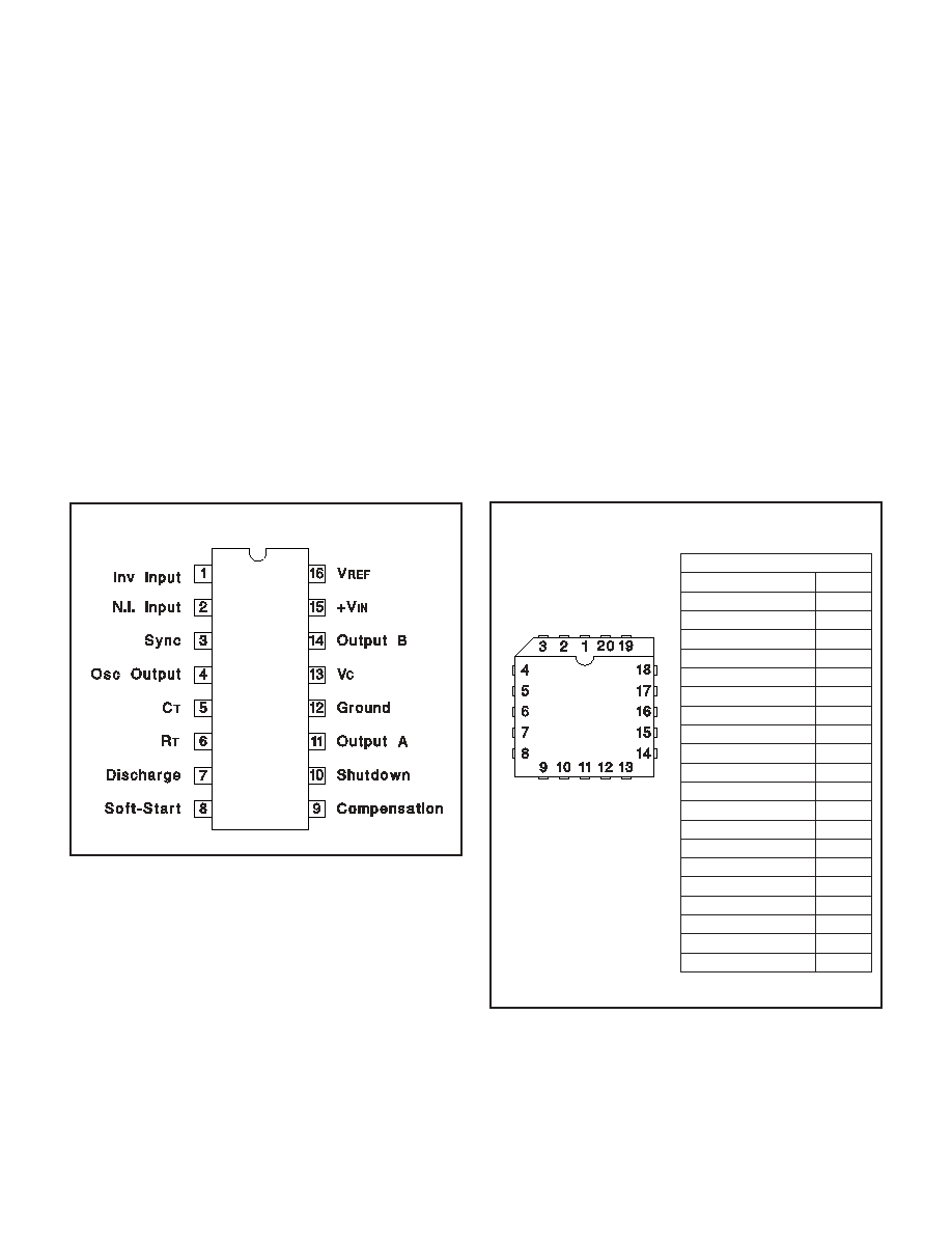
DIL-16 (TOP VIEW)
J or N Package
PLCC-20, LCC-20 (TOP VIEW)
Q, L Package
PACKAGE PIN FUNCTION
FUNCTION
PIN
N/C
1
Inv. Input
2
N.I. Input
3
SYNC
4
OSC. output
5
N/C
6
C
T
7
R
T
8
Discharge
9
Softstart
10
N/C
11
Compensation
12
Shutdown
13
Output A
14
Ground
15
N/C
16
V
C
17
Output B
18
+V
IN
19
V
REF
20
CONNECTION DIAGRAMS

3
UC1525A/27A
UC2525A/27A
UC3525A/27A
ELECTRICAL CHARACTERISTICS:
+V
IN
= 20V, and over operating temperature, unless otherwise specified, T
A
= T
J.
PARAMETER
TEST CONDITIONS
UC1525A/UC2525A
UC1527A/UC2527A
UC3525A
UC3527A
UNITS
MIN
TYP
MAX
MIN
TYP
MAX
Reference Section
Output Voltage
T
J
= 25∞C
5.05
5.10
5.15
5.00
5.10
5.20
V
Line Regulation
V
IN
= 8 to 35V
10
20
10
20
mV
Load Regulation
I
L
= 0 to 20mA
20
50
20
50
mV
Temperature Stability (Note 5)
Over Operating Range
20
50
20
50
Total Output Variation (Note 5)
Line, Load, and Temperature
5.00
5.20
4.95
5.25
V
Shorter Circuit Current
V
REF
= 0, T
J
= 25∞C
80
100
80
100
mA
Output Noise Voltage (Note 5)
10Hz 10kHz, T = 25 C
J
∞
40
200
40
200
µVrms
Long Term Stability (Note 5)
T
J
= 125∞C
20
50
20
50
mV
Oscillator Section(Note 6)
Initial Accuracy (Notes 5 & 6)
T
J
= 25∞C
± 2
± 6
± 2
± 6
%
Voltage Stability (Notes 5 & 6)
V
IN
= 8 to 35V
± 0.3
± 1
± 1
± 2
%
Temperature Stability (Note 5)
Over Operating Range
± 3
± 6
± 3
± 6
%
Minimum Frequency
R
T
= 200k
, C
T
= 0.1
µ
F
120
120
Hz
Maximum Frequency
R
T
= 2k
, C
T
= 470pF
400
400
kHz
Current Mirror
I
RT
= 2mA
1.7
2.0
2.2
1.7
2.0
2.2
mA
Clock Amplitude (Notes 5 & 6)
3.0
3.5
3.0
3.5
V
Clock Width (Notes 5 & 6)
T
J
= 25∞C
0.3
0.5
1.0
0.3
0.5
1.0
µs
Sync Threshold
1.2
2.0
2.8
1.2
2.0
2.8
V
Sync Input Current
Sync Voltage = 3.5V
1.0
2.5
1.0
2.5
mA
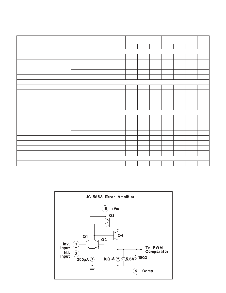
Error Amplifier Section
(V
CM
= 5.1V)
Input Offset Voltage
0.5
5
2
10
mV
Input Bias Current
1
10
1
10
µA
Input Offset Current
1
1
µA
DC Open Loop Gain
R
L
10M
60
75
60
75
dB
Gain-Bandwidth Product
(Note 5)
A
V
= 0dB, T
J
= 25∞C
1
2
1
2
MHz
DC Transconductance
(Notes 5 & 7)
T
J
= 25
∞
C, 30k
R
L
1M
1.1
1.5
1.1
1.5
mS
Output Low Level
0.2
0.5
0.2
0.5
V
Output High Level
3.8
5.6
3.8
5.6
V
Common Mode Rejection
V
CM
= 1.5 to 5.2V
60
75
60
75
dB
Supply Voltage Rejection
V
IN
= 8 to 35V
50
60
50
60
dB
Note 5: These parameters, although ensured over the recommended operating conditions, are not 100% tested in production.
Note 6: Tested at f
OSC
= 40kHz (R
T
= 3.6k
W, C
T
= 0.01
mF, R
D
= 0
W). Approximate oscillator frequency is defined by:
f
C
R
T
T
D
=
+
1
0.7
3R
(
)
Note 7: DC transconductance (g
M
) relates to DC open-loop voltage gain (A
V
) according to the following equation: A
V
= g
M
R
L
where R
L
is the resistance from pin 9 to ground
.
The minimum g
M
specification is used to calculate minimum A
V
when the
error amplifier output is loaded.
4
UC1525A/27A
UC2525A/27A
UC3525A/27A
ELECTRICAL CHARACTERISTICS:
+V
IN
= 20V, and over operating temperature, unless otherwise specified, T
A
= T
J.
PARAMETER
TEST CONDITIONS
UC1525A/UC2525A
UC1527A/UC2527A
UC3525A
UC3527A
UNITS
MIN
TYP
MAX
MIN
TYP
MAX
PWM Comparator
Minimum Duty-Cycle
0
0
%
Maximum Duty-Cycle (Note 6)
45
49
45
49
%
Input Threshold (Note 6)
Zero Duty-Cycle
0.7
0.9
0.7
0.9
V
Maximum Duty-Cycle
3.3
3.6
3.3
3.6
V
Input Bias Current (Note 5)
.05
1.0
.05
1.0
µA
Shutdown Section
Soft Start Current
V
SD
= 0V, V
SS
= 0V
25
50
80
25
50
80
µA
Soft Start Low Level
V
SD
= 2.5V
0.4
0.7
0.4
0.7
V
Shutdown Threshold
To outputs, V
SS
= 5.1V, T
J
= 25∞C
0.6
0.8
1.0
0.6
0.8
1.0
V
Shutdown Input Current
V
SD
= 2.5V
0.4
1.0
0.4
1.0
mA
Shutdown Delay (Note 5)
V
SD
= 2.5V, T
J
= 25∞C
0.2
0.5
0.2
0.5
µ
s
Output Drivers(Each Output) (V
C
= 20V)
Output Low Level
I
SINK
= 20mA
0.2
0.4
0.2
0.4
V
I
SINK
= 100mA
1.0
2.0
1.0
2.0
V
Output High Level
I
SOURCE
= 20mA
18
19
18
19
V
I
SOURCE
= 100mA
17
18
17
18
V
Under-Voltage Lockout
V
COMP
and V
SS
= High
6
7
8
6
7
8
V
V
C
OFF Current (Note 7)
V
C
= 35V
200
200
µA
Rise Time (Note 5)
C
L
= 1nF, T
J
= 25∞C
100
600
100
600
ns
Fall Time (Note 5)
C
L
= 1nF, T
J
= 25∞C
50
300
50
300
ns
Total Standby Current
Supply Current
V
IN
= 35V
14
20
14
20
mA
Note 5: These parameters, although ensured over the recommended operating conditions, are not 100% tested in production.
Note 6: Tested at f
OSC
= 40kHz (R
T
= 3.6k
W, C
T
= 0.01
mF, R
D
= 0
W)
Note 7: Collector off-state quiescent current measured at pin 13 with outputs low for UC1525A and high for UC1527A.
5
UC1525A/27A
UC2525A/27A
UC3525A/27A
PRINCIPLES OF OPERATION AND TYPICAL CHARACTERISTICS
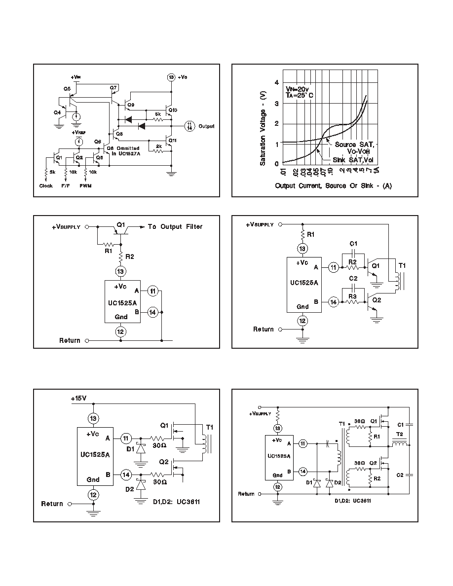
UC1525A output circuit (1/2 circuit shown).
UC1525A output saturation characteristics.
For single-ended supplies, the driver outputs are
grounded. The V
C
terminal is switched to ground by the
totem-pole source transistors on alternate oscillator
cycles.
In conventional push-pull bipolar designs, forward base
drive is controlled by R1-R3. Rapid turn-off times for the
power devices are achieved with speed-up capacitors
C1 and C2.
The low source impedance of the output drivers provides
rapid charging of power FET Input capacitance while
minimizing external components.
Low power transformers can be driven by the UC1525A.
Automatic reset occurs during dead time, when both
ends of the primary winding are switched to ground.
6
UC1525A/27A
UC2525A/27A
UC3525A/27A
PRINCIPLES OF OPERATION AND TYPICAL CHARAC-
TERISTIC SHUTDOWN OPTIONS
(See Block Diagram)
Since both the compensation and soft-start terminals
(Pins 9 and 8) have current source pull-ups, either can
readily accept a pull-down signal which only has to sink a
maximum of 100
µ
A to turn off the outputs. This is subject
to the added requirement of discharging whatever exter-
nal capacitance may be attached to these pins.
An alternate approach is the use of the shutdown circuitry
of Pin 10 which has been improved to enhance the avail-
able shutdown options. Activating this circuit by applying
a positive signal on Pin 10 performs two functions; the
PWM latch is immediately set providing the fastest
turn-off signal to the outputs; and a 150
µ
A-current sink
begins to discharge the external soft-start capacitor. If the
shutdown command is short, the PWM signal is termi-
nated without significant discharge of the soft-start ca-
pacitor, thus, allowing, for example, a convenient
implementation of pulse-by-pulse current limiting. Holding
Pin 10 high for a longer duration, however, will ultimately
discharge this external capacitor, recycling slow turn-on
upon release.
Pin 10 should not be left floating as noise pickup could
conceivably interrupt normal operation. All transitions of
the voltage on pin 10 should be within the time frame of
one clock cycle and not repeated at a frequency higher
than 10 clock cycles.
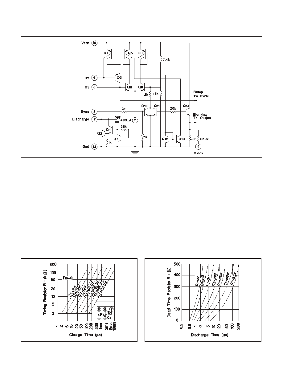
UC1525A oscillator schematic.
Oscillator Charge Time vs R
T
and C
T
.
Oscillator Discharge Time vs R
D
and C
T
.
7
UC1525A/27A
UC2525A/27A
UC3525A/27A
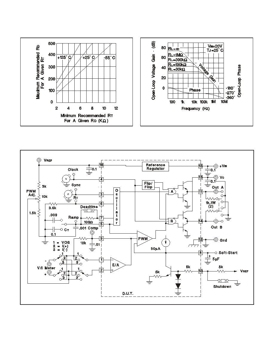
Lab test fixture.
Maximum value R
D
vs minimum value R
T
.
R
L
is impedance from pin 9 to ground. Values below 30k
will begin to limit the maximum duty cycle.
Error amplifier voltage gain and phase vs frequency.

8
UC1525A/27A
UC2525A/27A
UC3525A/27A
REVISION
DATE
CHANGE
SLUS191B
6/28/05
Updated pin 10 description in the Principles of Operation and Typical
Characteristics Shutdown Options Section.
REVISION HISTORY

IMPORTANT NOTICE
Texas Instruments Incorporated and its subsidiaries (TI) reserve the right to make corrections, modifications,
enhancements, improvements, and other changes to its products and services at any time and to discontinue
any product or service without notice. Customers should obtain the latest relevant information before placing
orders and should verify that such information is current and complete. All products are sold subject to TI's terms
and conditions of sale supplied at the time of order acknowledgment.
TI warrants performance of its hardware products to the specifications applicable at the time of sale in
accordance with TI's standard warranty. Testing and other quality control techniques are used to the extent TI
deems necessary to support this warranty. Except where mandated by government requirements, testing of all
parameters of each product is not necessarily performed.
TI assumes no liability for applications assistance or customer product design. Customers are responsible for
their products and applications using TI components. To minimize the risks associated with customer products
and applications, customers should provide adequate design and operating safeguards.
TI does not warrant or represent that any license, either express or implied, is granted under any TI patent right,
copyright, mask work right, or other TI intellectual property right relating to any combination, machine, or process
in which TI products or services are used. Information published by TI regarding third-party products or services
does not constitute a license from TI to use such products or services or a warranty or endorsement thereof.
Use of such information may require a license from a third party under the patents or other intellectual property
of the third party, or a license from TI under the patents or other intellectual property of TI.
Reproduction of information in TI data books or data sheets is permissible only if reproduction is without
alteration and is accompanied by all associated warranties, conditions, limitations, and notices. Reproduction
of this information with alteration is an unfair and deceptive business practice. TI is not responsible or liable for
such altered documentation.
Resale of TI products or services with statements different from or beyond the parameters stated by TI for that
product or service voids all express and any implied warranties for the associated TI product or service and
is an unfair and deceptive business practice. TI is not responsible or liable for any such statements.
Following are URLs where you can obtain information on other Texas Instruments products and application
solutions:
Products
Applications
Amplifiers
amplifier.ti.com
Audio
www.ti.com/audio
Data Converters
dataconverter.ti.com
Automotive
www.ti.com/automotive
DSP
dsp.ti.com
Broadband
www.ti.com/broadband
Interface
interface.ti.com
Digital Control
www.ti.com/digitalcontrol
Logic
logic.ti.com
Military
www.ti.com/military
Power Mgmt
power.ti.com
Optical Networking
www.ti.com/opticalnetwork
Microcontrollers
microcontroller.ti.com
Security
www.ti.com/security
Telephony
www.ti.com/telephony
Video & Imaging
www.ti.com/video
Wireless
www.ti.com/wireless
Mailing Address:
Texas Instruments
Post Office Box 655303 Dallas, Texas 75265
Copyright
2005, Texas Instruments Incorporated