 | –≠–ª–µ–∫—Ç—Ä–æ–Ω–Ω—ã–π –∫–æ–º–ø–æ–Ω–µ–Ω—Ç: UC1526AJ | –°–∫–∞—á–∞—Ç—å:  PDF PDF  ZIP ZIP |
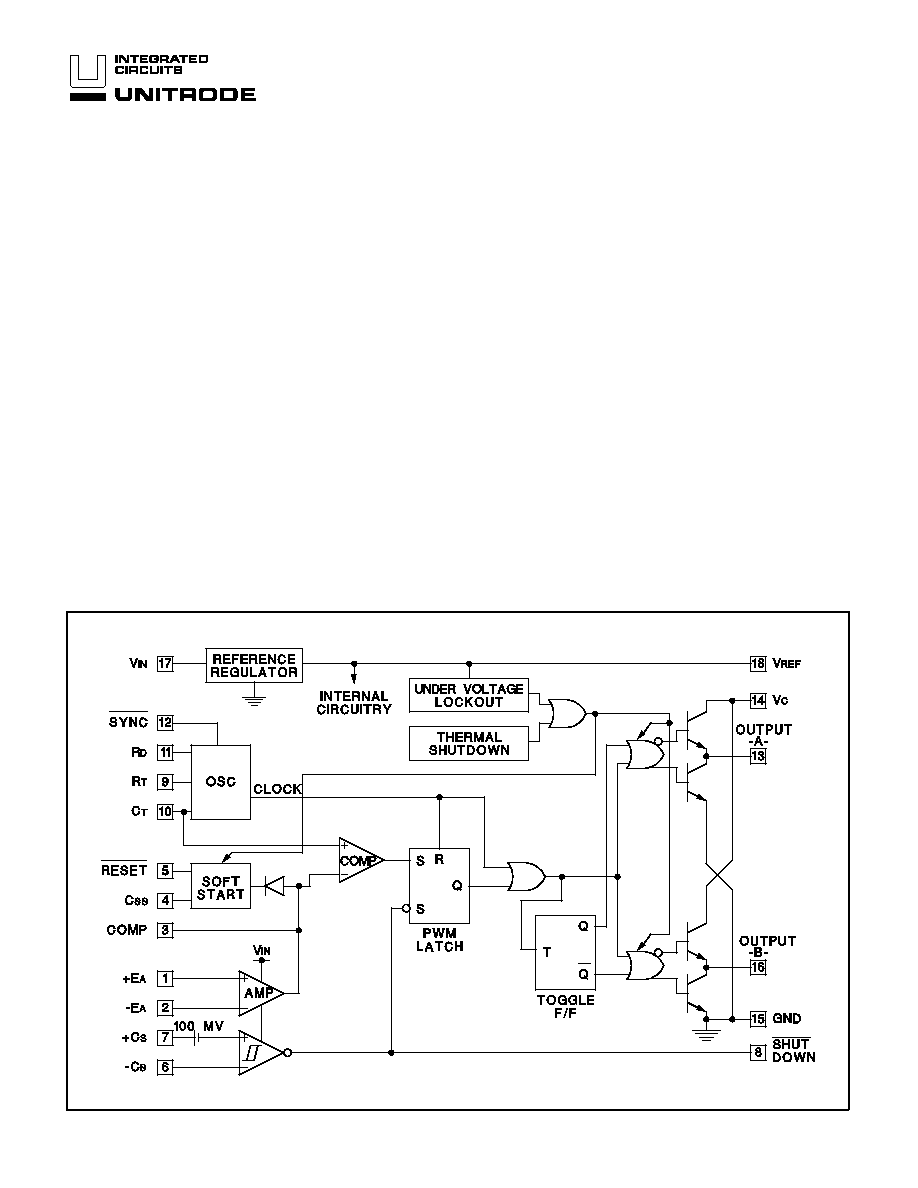
BLOCK DIAGRAM
UC1526A
UC2526A
UC3526A
Regulating Pulse Width Modulator
FEATURES
∑
Reduced Supply Current
∑
Oscillator Frequency to 600kHz
∑
Precision Band-Gap Reference
∑
7 to 35V Operation
∑
Dual 200mA Source/Sink Outputs
∑
Minimum Output Cross-Conduction
∑
Double-Pulse Suppression Logic
∑
Under-Voltage Lockout
∑
Programmable Soft-Start
∑
Thermal Shutdown
∑
TTL/CMOS Compatible Logic Ports
∑
5 Volt Operation (V
IN
= V
C
= V
REF
= 5.0V)
DESCRIPTION
The UC1526A Series are improved-performance pulse-width modu-
lator circuits intended for direct replacement of equivalent non- "A"
versions in all applications. Higher frequency operation has been
enhanced by several significant improvements including: a more ac-
curate oscillator with less minimum dead time, reduced circuit de-
lays (particularly in current limiting), and an improved output stage
with negligible cross-conduction current. Additional improvements
include the incorporation of a precision, band-gap reference gener-
ator, reduced overall supply current, and the addition of thermal
shutdown protection.
Along with these improvements, the UC1526A Series retains the
protective features of under-voltage lockout, soft-start, digital cur-
rent limiting, double pulse suppression logic, and adjustable
deadtime. For ease of interfacing, all digital control ports are TTL
compatible with active low logic.
Five volt (5V) operation is possible for "logic level" applications by
connecting V
IN,
V
C
and V
REF
to a precision 5V input supply. Consult
factory for additional information.
6/93
RECOMMENDED OPERATING CONDITIONS
(Note 3)
Input Voltage . . . . . . . . . . . . . . . . . . . . . . . . . . . . . . +7V to +35V
Collector Supply Voltage . . . . . . . . . . . . . . . . . . +4.5V to +35V
Sink/Source Load Current (each output) . . . . . . . . 0 to 100mA
Reference Load Current . . . . . . . . . . . . . . . . . . . . . . 0 to 20mA
Oscillator Frequency Range . . . . . . . . . . . . . . . . 1Hz to 600kHz
Oscillator Timing Resistor. . . . . . . . . . . . . . . . . . . 2k
to 150k
Oscillator Timing Capacitor. . . . . . . . . . . . . . . . . 400pF to 20
µ
F
Available Deadtime Range at 40kHz . . . . . . . . . . . . 1% to 50%
Operating Ambient Temperature Range
UC1526A. . . . . . . . . . . . . . . . . . . . . . . . . . . . -55∞C to +125∞C
UC2526A. . . . . . . . . . . . . . . . . . . . . . . . . . . . . -25∞C to +85∞C
UC3526A. . . . . . . . . . . . . . . . . . . . . . . . . . . . . . . 0∞C to +70∞C
ABSOLUTE MAXIMUM RATINGS (Note 1, 2)
Input Voltage (+V
IN)
. . . . . . . . . . . . . . . . . . . . . . . . . . . . . . +40V
Collector Supply Voltage (+V
C
) . . . . . . . . . . . . . . . . . . . . . +40V
Logic Inputs . . . . . . . . . . . . . . . . . . . . . . . . . . . . -0.3V to +5.5V
Analog Inputs . . . . . . . . . . . . . . . . . . . . . . . . . . . . -0.3V to +V
IN
Source/Sink Load Current (each output) . . . . . . . . . . . . 200mA
Reference Load Current . . . . . . . . . . . . . . . . . . . . . . . . . . 50mA
Logic Sink Current . . . . . . . . . . . . . . . . . . . . . . . . . . . . . . 15mA
Power Dissipation at T
A
= +25∞C (Note 2) . . . . . . . . . 1000mW
Power Dissipation at T
C
= +25∞C (Note 2) . . . . . . . . . . 3000mW
Operating Junction Temperature . . . . . . . . . . . . . . . . . . +150∞C
Storage Temperature Range . . . . . . . . . . . . . . -65∞C to +150∞C
Lead Temperature (soldering, 10 seconds) . . . . . . . . . . +300∞C
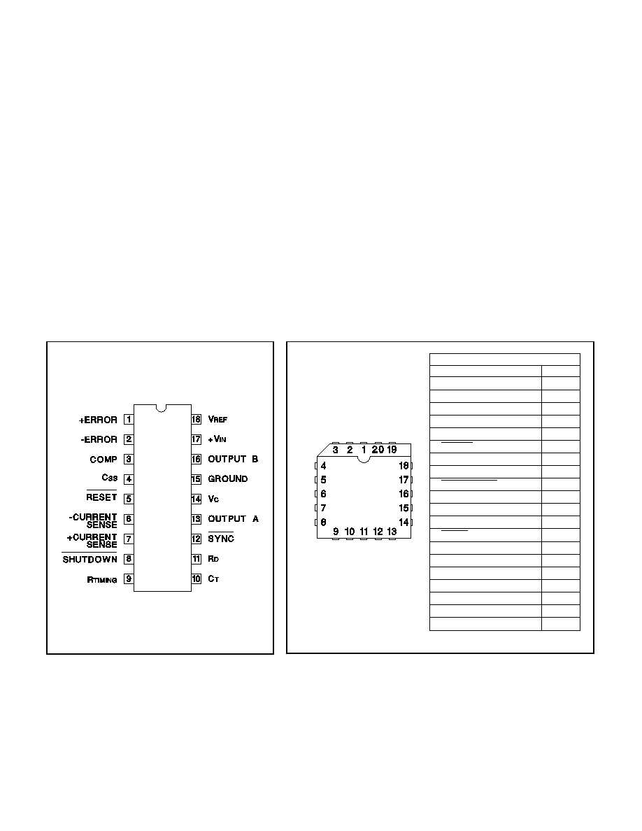
CONNECTION DIAGRAMS
PACKAGE PIN FUNCTION
FUNCTION
PIN
N/C
1
+ERROR
2
-ERROR
3
COMP.
4
C
SS
5
RESET
6
- CURRENT SENSE
7
+ CURRENT SENSE
8
SHUTDOWN
9
R
TIMING
10
C
T
11
R
D
12
SYNC
13
OUTPUT A
14
V
C
15
N/C
16
GROUND
17
OUTPUT B
18
+V
IN
19
V
REF
20
PLCC-20, LCC-20
(TOP VIEW)
Q and L Packages
DIL-18, SOIC-18 (TOP VIEW)
J or N Package, DW Package
Note 1: Values beyond which damage may occur.
Note 2: Consult packaging Section of Databook for thermal
limitations and considerations of package.
Note 3: Range over which the device is functional and
parameter limits are guaranteed.
UC1526A
UC2526A
UC3526A
2
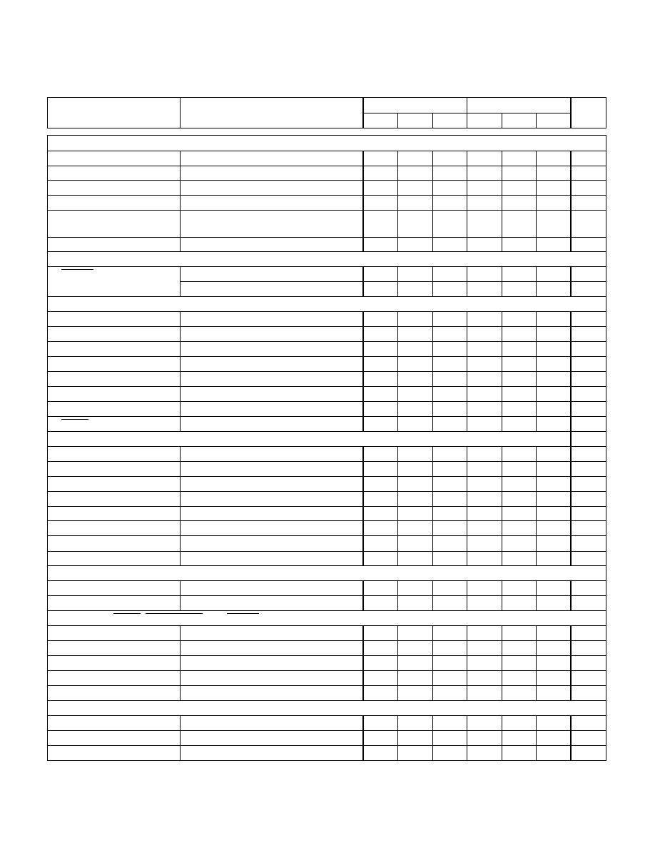
PARAMETER
TEST CONDITIONS
UC1526A / UC2526A
UC3526A
UNITS
MIN
TYP
MAX
MIN
TYP
MAX
Reference Section (Note 4)
Output Voltage
T
J
= +25∞C
4.95
5.00
5.05
4.90
5.00
5.10
V
Line Regulation
+V
IN
= 7 to 35V
2
10
2
15
mV
Load Regulation
I
L
= 0 to 20mA
5
20
5
20
mV
Temperature Stability
Over Operating T
J
(Note 5)
15
50
15
50
mV
Total Output Voltage
Range
Over Recommended Operating
Conditions
4.90
5.00
5.10
4.85
5.00
5.15
V
Short Circuit Current
V
REF
= 0V
25
50
100
25
50
100
mA
Under-Voltage Lockout
RESET Output Voltage
V
REF
= 3.8V
0.2
0.4
0.2
0.4
V
V
REF
= 4.7V
2.4
4.7
2.4
4.8
V
Oscillator Section (Note 6)
Initial Accuracy
T
J
= +25∞C
±
3
±
8
±
3
±
8
%
Voltage Stability
+V
IN
= 7 to 35V
0.5
1
0.5
1
%
Temperature Stability
Over Operating T
J
(Note 5)
2
6
1
3
%
Minimum Frequency
R
T
= 150k
, C
T
= 20
µ
F (Note 5)
1
1
Hz
Maximum Frequency
R
T
= 2k
, C
T
= 470pF
550
650
kHz
Sawtooth Peak Voltage
+V
IN
= 35V
3.0
3.5
3.0
3.5
V
Sawtooth Valley Voltage
+V
IN
=7V
0.5
1.0
0.5
1.0
V
SYNC Pulse Width
T
J =
25∞C, R
L
= 2.7k
to V
REF
1.1
1.1
µ
s
Error Amplifier Section (Note 7)
Input Offset Voltage
R
S
2k
2
5
2
10
mV
Input Bias Current
-350
-1000
-350
-2000
nA
Input Offset Current
35
100
35
200
nA
DC Open Loop Gain
R
L
10M
64
72
60
72
dB
HIGH Output Voltage
V
PIN 1
- V
PIN 2
150mV, I
SOURCE
= 100
µ
A
3.6
4.2
3.6
4.2
V
LOW Output Voltage
V
PIN 2
- V
PIN 1
150mV, I
SINK
= 100
µ
A
0.2
0.4
0.2
0.4
V
Common Mode Rejection
R
S
2k
70
94
70
94
dB
Supply Voltage Rejection
+V
IN
= 12 to 18V
66
80
66
80
dB
PWM Comparator (Note 6)
Minimum Duty Cycle
V
COMPENSATION
= +0.4V
0
0
%
Maximum Duty Cycle
V
COMPENSATION
= +3.6V
45
49
45
49
%
Digital Ports (SYNC, SHUTDOWN, and RESET)
HIGH Output Voltage
I
SOURCE
= 40
µ
A
2.4
4.0
2.4
4.0
V
LOW Output Voltage
I
SINK
= 3.6mA
0.2
0.4
0.2
0.4
V
HIGH Input Current
V
IH
= +2.4V
-125
-200
-125
-200
µ
A
LOW Input Current
V
IL
= +0.4V
-225
-360
-225
-360
µ
A
Shutdown Delay
From Pin 8, T
J
= 25∞C
160
160
ns
Current Limit Comparator (Note 8)
Sense Voltage
R
S
50
90
100
110
80
100
120
mV
Input Bias Current
-3
-10
-3
-10
µ
A
Shutdown Delay
From pin 7, 100mV Overdrive, T
J
= 25∞C
260
260
ns
+V
IN
= 15V, and over operating ambient temperature, unless otherwise specified T
A
= T
J.
ELECTRICAL CHARACTERISTICS:
Note 4: I
L =
0mA.
Note 5: Guaranteed by design, not 100% tested in production.
Note 6: F
OSC
= 40kHz, (R
T
= 4.12k
±
1%, C
T
= 0.01
µ
F
±
1%,
R
D
= 0
).
Note 7: V
CM
= 0 to +5.2V
Note 8: V
CM
= 0 to +12V.
Note 9: V
C
= +15V.
Note 10:V
IN
= +35V, R
T
= 4.12k
.
UC1526A
UC2526A
UC3526A
3
ELECTRICAL CHARACTERISTICS:
PARAMETER
TEST CONDITIONS
UC1526A
UC2526A
UC3526A
UNITS
MIN
TYP
MAX
MIN
TYP
MAX
Soft-Start Section
Error Clamp Voltage
RESET = +0.4V
0.1
0.4
0.1
0.4
V
C
S
Charging Current
RESET = +2.4V
50
100
150
50
100
150
µ
A
Output Drivers (Each Output) (Note 9)
HIGH Output Voltage
I
SOURCE
= 20mA
12.5
13.5
12.5
13.5
V
I
SOURCE
= 100mA
12
13
12
13
V
LOW Output Voltage
I
SINK
= 20mA
0.2
0.3
0.2
0.3
V
I
SINK
= 100mA
1.2
2.0
1.2
2.0
V
Collector Leakage
V
C
= 40V
50
150
50
150
µ
A
Rise Time
C
L
= 1000pF (Note 5)
0.3
0.6
0.3
0.6
µ
s
Fall Time
C
L
= 1000pF (Note 5)
0.1
0.2
0.1
0.2
µ
s
Cross-Conduction Charge
Per cycle, T
J
= 25∞C
8
8
nC
Power Consumption (Note 10)
Standby Current
SHUTDOWN = +0.4V
14
20
14
20
mA
Note 4: I
L =
0mA.
Note 5: Guaranteed by design, not 100% tested in production.
Note 6: F
OSC
= 40kHz, (R
T
= 4.12k
±
1%, C
T
= 0.01
µ
F
±
1%,
R
D
= 0
).
Note 7: V
CM
= 0 to +5.2V
Note 8: V
CM
= 0 to +12V.
Note 9: V
C
= +15V.
Note 10:V
IN
= +35V, R
T
= 4.12k
.
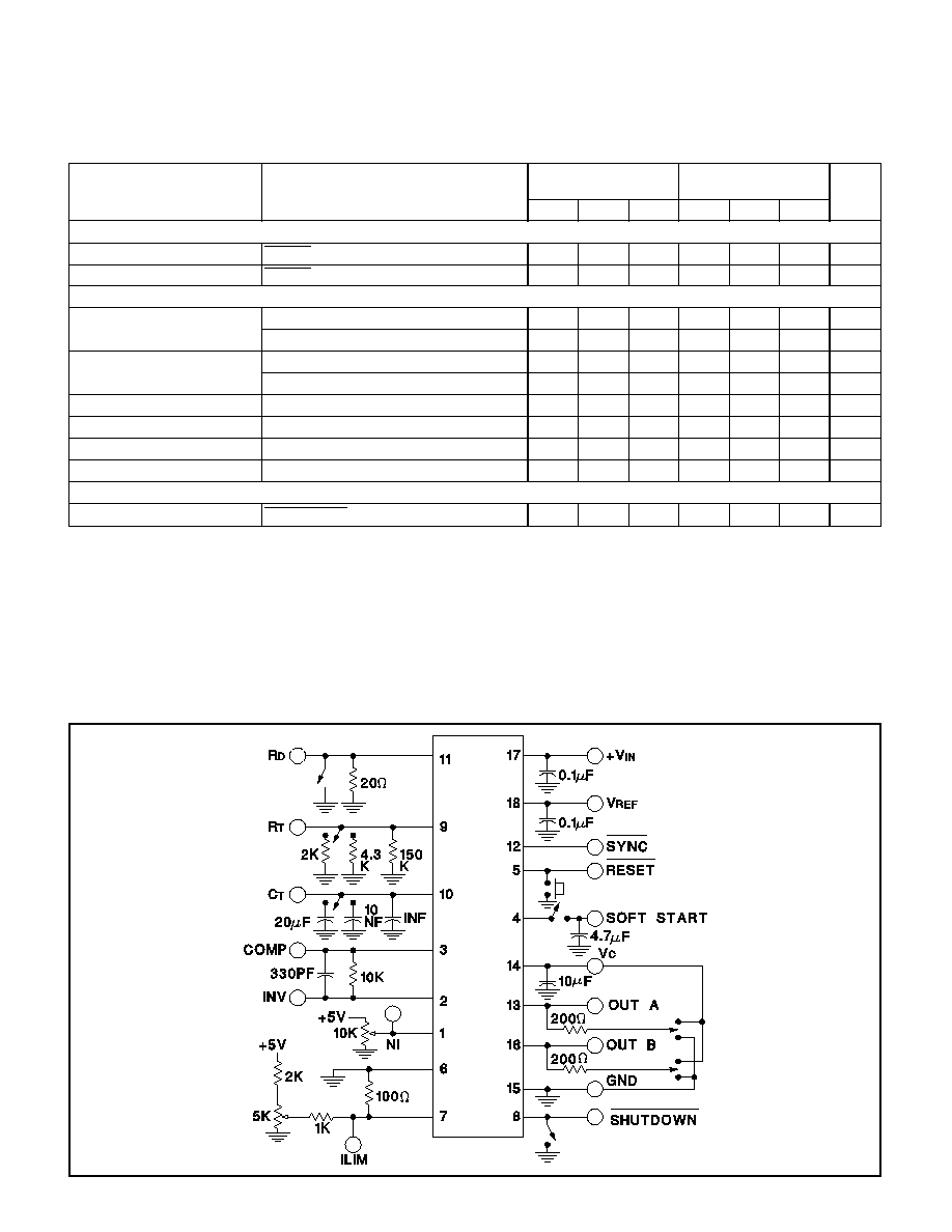
Open Loop Test Circuit UC1526A
+V
IN
= 15V, and over operating ambient temperature, unless otherwise specified T
A
= T
J.
UC1526A
UC2526A
UC3526A
4
APPLICATIONS INFORMATION
Voltage Reference
The reference regulator of the UC1526A is based on a
precision band-gap reference, internally trimmed to
±
1%
accuracy. The circuitry is fully active at supply voltages
above +7V, and provides up to 20mA of load current to
external circuitry at +5.0V. In systems where additional
current is required, an external PNP transistor can be
used to boost the available current. A rugged low fre-
quency audio-type transistor should be used, and lead
lengths between the PWM and transistor should be as
short as possible to minimize the risk of oscillations.
Even so, some types of transistors may require collec-
tor-base capacitance for stability. Up to 1 amp of load
current can be obtained with excellent regulation if the
device selected maintains high current gain.
Soft-Start Circuit
The soft-start circuit protects the power transistors and
rectifier diodes from high current surges during power
supply turn-on. When supply voltage is first applied to
the UC1526A, the under-voltage lockout circuit holds
RESET LOW with Q
3
. Q
1
is turned on, which holds the
soft-start capacitor voltage at zero. The second collector
of Q
1
clamps the output of the error amplifier to ground,
guaranteeing zero duty cycle at the driver outputs.
When the supply voltage reaches normal operating
range, RESET will go HIGH. Q
1
turns off, allowing the
internal 100
µ
A current source to charge C
S
. Q
2
clamps
the error amplifier output to 1V
BE
above the voltage on
C
S
. As the soft-start voltage ramps up to +5V, the duty
cycle of the PWM linearly increases to whatever value
the voltage regulation loop requires for an error null.
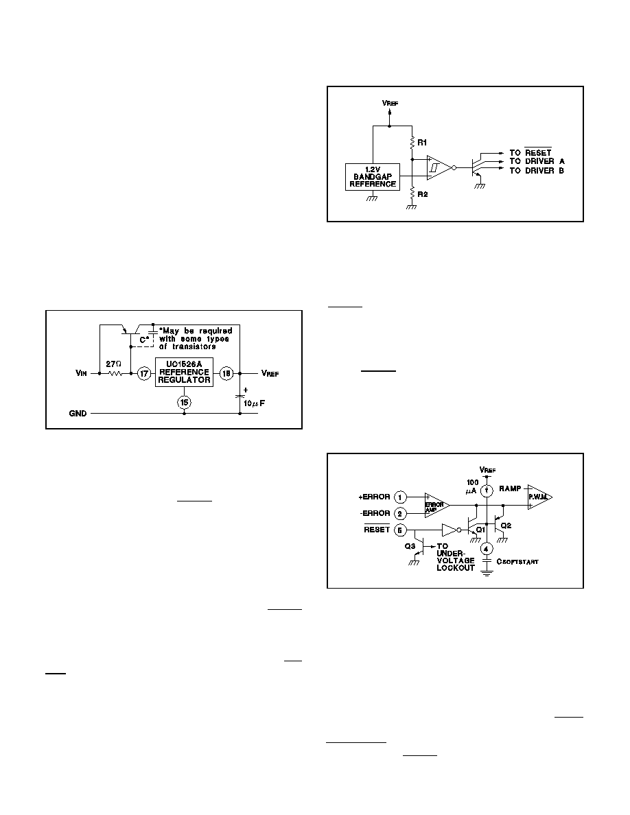
Under-Voltage Lockout
The under-voltage lockout circuit protects the UC1526A
and the power devices it controls from inadequate sup-
ply voltage, If +V
IN
is too low, the circuit disables the
output drivers and holds the RESET pin LOW. This pre-
vents spurious output pulses while the control circuitry is
stabilizing, and holds the soft-start timing capacitor in a
discharged state.
The circuit consists of a +1.2V bandgap reference and
comparator circuit which is active when the reference
voltage has risen to 3V
BE
or +1.8V at 25∞C. When the
reference voltage rises to approximately +4.4V, the cir-
cuit enables the output drivers and releases the RESET
pin, allowing a normal soft-start. The comparator has
350mV of hysteresis to minimize oscillation at the trip
point. When +V
IN
to the PWM is removed and the refer-
ence drops to +4.2V, the under-voltage circuit pulls RE-
SET LOW again. The soft-start capacitor is immediately
discharged, and the PWM is ready for another soft-start
cycle.
The UC1526A can operate from a +5V supply by con-
necting the V
REF
pin to the +V
IN
pin and maintaining the
supply between +4.8 and +5.2V.
Digital Control Ports
The three digital control ports of the UC1526A are bi-di-
rectional. Each pin can drive TTL and 5V CMOS logic di-
rectly, up to a fan-out of 10 low-power Schottky gates.
Each pin can also be directly driven by open-collector
TTL, open-drain CMOS, and open-collector voltage
comparators; fan-in is equivalent to 1 low-power Schot-
tky gate. Each port is normally HIGH; the pin is pulled
LOW to activate the particular function. Driving SYNC
LOW initiates a discharge cycle in the oscillator. Pulling
SHUTDOWN LOW immediately inhibits all PWM output
pulses. Holding RESET LOW discharges the soft-start
Figure 1.
Extending Reference Output Current
Figure 2.
Under-Voltage Lockout Schematic
Figure 3.
Soft-Start Circuit Schematic
UC1526A
UC2526A
UC3526A
5