 | –≠–ª–µ–∫—Ç—Ä–æ–Ω–Ω—ã–π –∫–æ–º–ø–æ–Ω–µ–Ω—Ç: UC1707L | –°–∫–∞—á–∞—Ç—å:  PDF PDF  ZIP ZIP |
UC1707
UC2707
UC3707
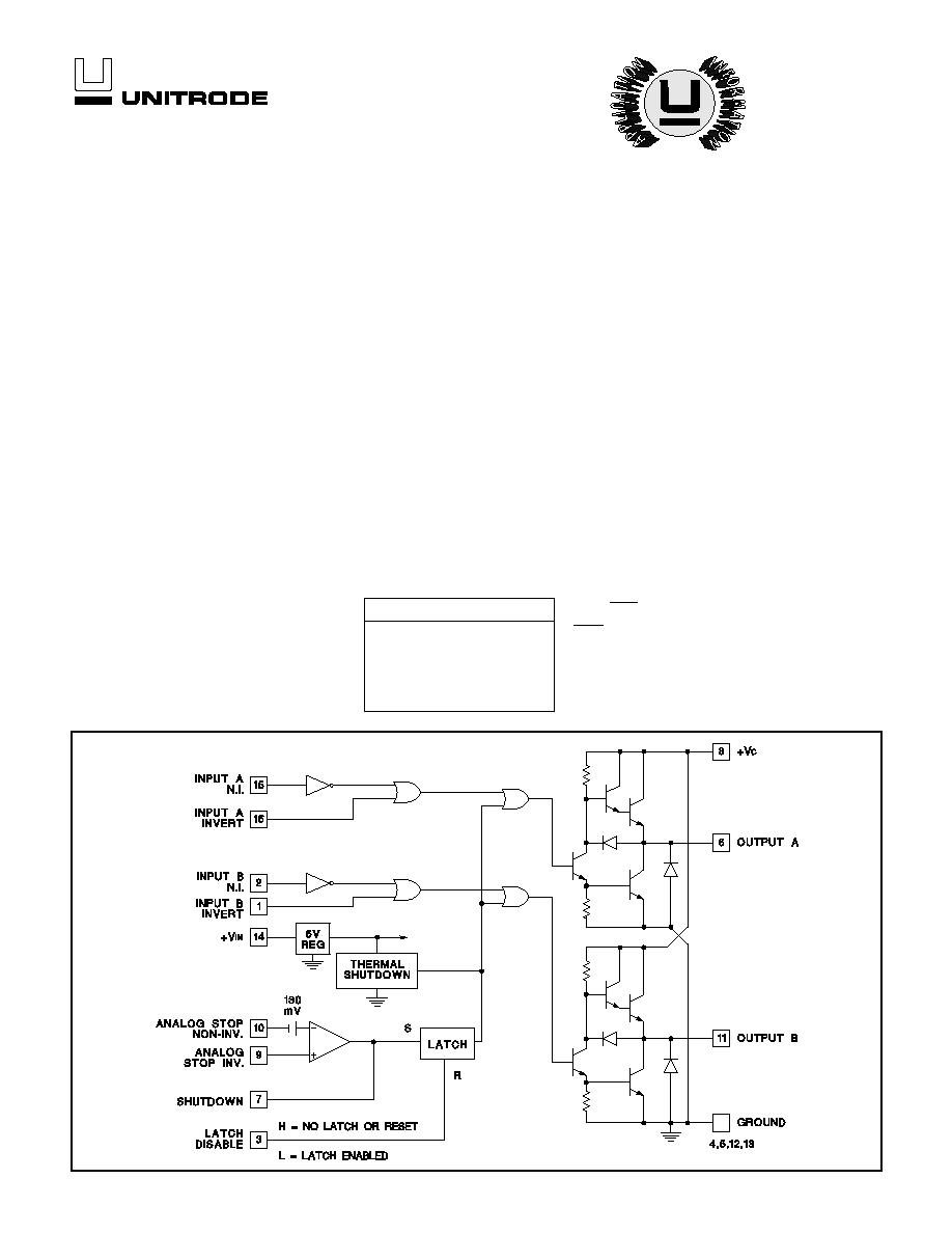
DESCRIPTION
The UC1707 family of power drivers is made with a high-speed Schottky
process to interface between low-level control functions and high-power
switching devices - particularly power MOSFETs. These devices contain
two independent channels, each of which can be activated by either a high
or low input logic level signal. Each output can source or sink up to 1.5A as
long as power dissipation limits are not exceeded.
Although each output can be activated independently with its own inputs, it
can be forced low in common through the action either of a digital high sig-
nal at the Shutdown terminal or a differential low-level analog signal. The
Shutdown command from either source can either be latching or not, de-
pending on the status of the Latch Disable pin.
Supply voltage for both VIN and VC can independently range from 5V to
40V.
These devices are available in two-watt plastic "bat-wing" DIP for operation
over a 0∞C to 70∞C temperature range and, with reduced power, in a her-
metically sealed cerdip for ≠55∞C to +125∞C operation. Also available in
surface mount DW, Q, L packages.
Dual Channel Power Driver
FEATURES
∑
Two independent Drivers
∑
1.5A Totem Pole Outputs
∑
Inverting and Non-Inverting Inputs
∑
40ns Rise and Fall into 1000pF
∑
High-Speed, Power MOSFET
Compatible
∑
Low Cross-Conduction Current Spike
∑
Analog Shutdown with Optional Latch
∑
Low Quiescent Current
∑
5V to 40V Operation
∑
Thermal Shutdown Protection
∑
16-Pin Dual-In-Line Package
∑
20-Pin PLCC and CLCC Package
03/99
BLOCK DIAGRAM
INV.
N.I.
OUT
OUT = INV and N.I.
H
H
L
OUT = INV or N.I.
L
H
H
H
L
L
L
L
L
TRUTH TABLE (Each Channel)
2
UC1707
UC2707
UC3707
Supply Voltage, VIN, N/J-Pkg . . . . . . . . . . . . . . . . . . . . . . . 40V
Collector Supply Voltage, VC, N/J-Pkg . . . . . . . . . . . . . . . 40V
Output Current (Each Output, Source or Sink) Steady-State,
N/J-Pkg. . . . . . . . . . . . . . . . . . . . . . . . . . . . . . . . . . . ±500mA
Peak Transient
N-Pkg . . . . . . . . . . . . . . . . . . . . . . . . . . . . . . . . . . . . . . ±1.5A
J-Pkg . . . . . . . . . . . . . . . . . . . . . . . . . . . . . . . . . . . . . . ±1.0A
Capacitive Discharge Energy
N-Pkg . . . . . . . . . . . . . . . . . . . . . . . . . . . . . . . . . . . . . . 20mJ
J-Pkg . . . . . . . . . . . . . . . . . . . . . . . . . . . . . . . . . . . . . . . 15mJ
Digital Inputs (See Note), N/J-Pkg . . . . . . . . . . . . . . . . . . . 5.5V
Analog Stop Inputs, N/J-Pkg . . . . . . . . . . . . . . . . . . . . . . . . VIN
Power Dissipation at T
A
= 25∞C (See Note)
N-Pkg . . . . . . . . . . . . . . . . . . . . . . . . . . . . . . . . . . . . . . . . 2W
J-Pkg . . . . . . . . . . . . . . . . . . . . . . . . . . . . . . . . . . . . . . . . 1W
Power Dissipation at T (Leads/Case) = 25∞C (See Note)
N-Pkg . . . . . . . . . . . . . . . . . . . . . . . . . . . . . . . . . . . . . . . . 5W
J-Pkg . . . . . . . . . . . . . . . . . . . . . . . . . . . . . . . . . . . . . . . . 2W
Operating Temperature Range . . . . . . . . . . . . ≠55∞C to +125∞C
Storage Temperature Range . . . . . . . . . . . . . ≠65∞C to +150∞C
Lead Temperature (Soldering, 10 Seconds) . . . . . . . . . . 300∞C
ABSOLUTE MAXIMUM RATINGS
Note: All voltages are with respect to the four ground pins
which must be connected together. All currents are positive
into, negative out of the specified terminal. Digital Drive can ex-
ceed 5.5V if input current is limited to 10mA. Consult Pack-
aging
section
of
Databook
for
thermal
limitations
and
considerations of package.
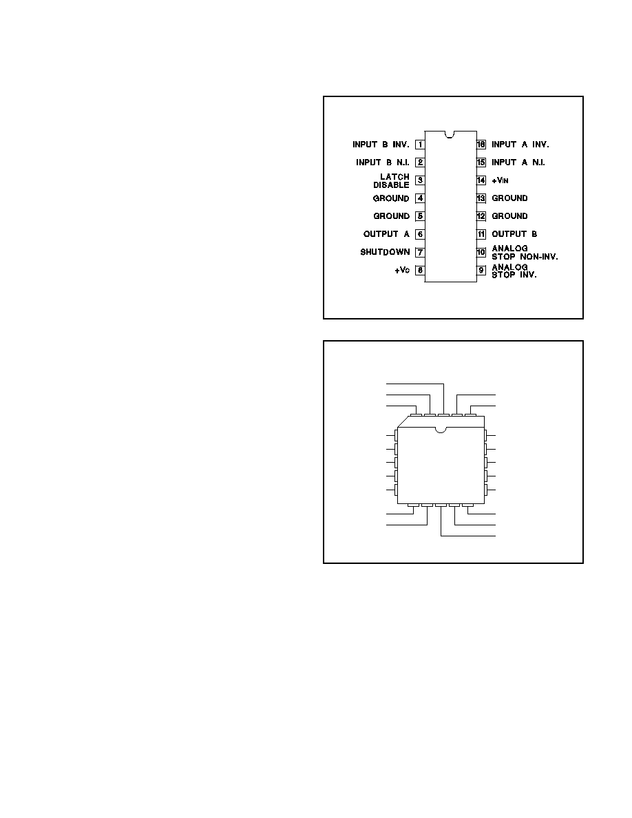
CONNECTION DIAGRAMS
DIL-16, SOIC-16 (TOP VIEW)
J or N Package,
3
18
17
16
N/C
1
2
20 19
15
14
4
5
6
7
8
9
11
10
12 13
INPUT B INV.
INPUT B I.N.
INPUT A INV.
INPUT A NON INV.
VIN
GROUND
N/C
GROUND
OUTPUT B
LATCH DISABLE
GROUND
N/C
GROUND
OUTPUT A
ANALOG STOP INV.
ANALOG STOP NON INV.
N/C
SHUTDOWN
VC
PLCC-20, LCC-20 (TOP VIEW)
Q, L Packages
Note: All four ground pins must be connected to a common
ground.

3
UC1707
UC2707
UC3707
ELECTRICAL CHARACTERISTICS:
Unless otherwise stated, these specifications apply for T
A
= ≠55∞C to +125∞C for
the UC1707, ≠25∞C to +85∞C for the UC2707 and 0∞C to +70∞C for the UC3707; V
IN
= V
C
= 20V. T
A
= T
J
.
PARAMETERS
TEST CONDITIONS
MIN
TYP
MAX
UNITS
V
IN
Supply Current
V
IN
= 40V
12
15
mA
V
C
Supply Current
V
C
= 40V, Outputs Low
5.2
7.5
mA
V
C
Leakage Current
V
IN
=0, VC =30V, No Load
.05
0.1
mA
Digital Input Low Level
0.8
V
Digital Input High Level
2.2
V
Input Current
V
I
= 0
≠0.06
≠1.0
mA
Input Leakage
V
I
= 5V
.05
0.1
mA
Output High Sat., V
C
-V
O
I
O
= ≠50mA
2.0
V
I
O
= ≠500mA
2.5
V
Output Low Sat., V
O
I
O
= ≠50mA
0.4
V
I
O
= ≠500mA
2.5
V
Analog Threshold
V
CM
= 0 to 15V
100
130
160
mV
Input Bias Current
V
CM
= 0
≠10
≠20
µ
A
Thermal Shutdown
155
∞
C
Shutdown Threshold
Pin 7 Input
0.4
1.0
2.2
V
Latch Disable Threshold
Pin 3 Input
0.8
1.2
2.2
V
TYPICAL SWITCHING CHARACTERISTICS:
V
IN
= V
C
= 20V, T
A
= 25∞C. Delays measured to 10% output change.
PARAMETERS
TEST CONDITIONS
OUTPUT CL =
UNITS
From Inv. Input to Output
open
1.0
2.2
nF
Rise Time Delay
40
50
60
ns
10% to 90% Rise
25
40
50
ns
Fall Time Delay
30
40
50
ns
90% to 10% Fall
25
40
50
ns
From N.I. Input to Output
Rise Time Delay
30
40
50
ns
10% to 90% Rise
25
40
50
ns
Fall Time Delay
45
55
65
ns
90% to 10% Fall
25
40
50
ns
V
C
Cross-Conduction
Current Spike Duration
Output Rise
25
ns
Output Fall
0
ns
Analog Shutdown Delay
Stop non-Inv. = 0V
180
ns
Stop Inv. = 0 to 0.5V
180
ns
Digital Shutdown Delay
2V Input on Pin 7
50
ns
4
UC1707
UC2707
UC3707
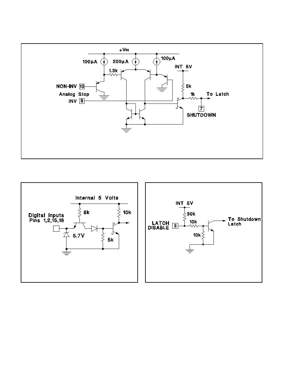
The input zener may be used to clamp input signal voltages
higher than 5V as long as the zener current is limited to
10mA max. External pull-up resistors are not required.
SIMPLIFIED INTERNAL CIRCUITRY
Figure 1. Typical digital input gate.
Figure 3. Latch disable.
The Shutdown latch is disabled when pin 3 is open. An im-
pedance of 4k or less from pin 3 to ground will allow a shut-
down signal to set the latch which can then be reset by
either recycling the VIN supply or by momentarily (>200ns)
raising pin 3 high.
The input common-mode voltage range is from ground to (VIN-3V). When not used both inputs shoul1d be grounded. Activate
time is a function of overdrive with a typical value of 180ns. Pin 7 serves both as a comparator output and as a common digital
shutdown input. A high signal here will accomplish the fastest turn off of both outputs. Note that "OFF" is defined as the outputs
low. Pulling shutdown low defeats the latch operation regardless of its status.
Figure 2. Typical digital input gate.

5
UC1707
UC2707
UC3707
Figure 5. Current limiting.
The Analog shutdown can give pulse-by-pulse current limiting with a reset pulse from the clock output of the UC1524. R1C1 is
used to filter leading edge spikes.
SIMPLIFIED INTERNAL CIRCUITRY (cont.)
Figure 4. Transformer coupled push-pull MOSFET drive circuit.