
UC1711
UC3711
03/99
Dual Ultra High-Speed FET Driver
FEATURES
∑
25ns Rise and Fall into 1000pF
∑
15ns Propagation Delay
∑
1.5A Source or Sink Output Drive
∑
Operation with 5V to 35V Supply
∑
High-Speed Schottky NPN Process
∑
8-PIN MINIDIP Package
DESCRIPTION
The UC1711 family of FET drivers are made with an
all-NPN Schottky process in order to optimize switching
speed, temperature stability, and radiation resistance.
The cost for these benefits is a quiescent supply current
which varies with both output state and supply voltage.
For lower power requirements, refer to the the UC1709
family which is both pin compatible with, and functionally
equivalent to the UC1711.
These devices implement inverting logic with TTL com-
patible inputs, and output stages which will either source,
or sink in excess of 1.5A of load current with minimal
cross-conduction charge. Due to their monolithic
con-
struction, the channels are well matched and can be par-
alleled for doubled output current capability.
4
2
7.5V REG
6
V
CC
7
A Out
3k
3
B Out
A
IN
2.5k
3k
2.5k
B
IN
5
Gnd
BLOCK DIAGRAM
CONNECTION DIAGRAM
UDG-99078
DIL-8 (Top View)
J or N Package
TEMPERATURE RANGE
PACKAGE
UC1711J
≠55∞C to +125∞C
Ceramic DIP
UC3711J
0∞C to +70∞C
Ceramic DIP
UC3711N
0∞C to +70∞C
Plastic DIP
ORDERING INFORMATION
ABSOLUTE MAXIMUM RATINGS
Input Supply Voltage, V
CC
. . . . . . . . . . . . . . . . . . . . . . . . . . 40V
Output Current (Source or Sink)
Steady State . . . . . . . . . . . . . . . . . . . . . . . . . . . . . .
±
500mA
Peak Transient . . . . . . . . . . . . . . . . . . . . . . . . . . . . . . . ± 1.5A
Maximum Forced Voltage . . . . . . . . . . . . . . . . . . . . -0.3V to 7V
Maximum Forced Current . . . . . . . . . . . . . . . . . . . . . . . ± 10mA
Power Dissipation . . . . . . . . . . . . . . . . . . . . . . . . . . . . . . . . 1W
Operating Junction Temperature . . . . . . . . . . ≠55∞C to +150∞C
Storage Temperature . . . . . . . . . . . . . . . . . . . ≠65∞C to +150∞C
Note 1: Unless otherwise indicated, voltages are reference to
ground and currents are positive into, negative out of, the spec-
ified terminals. All reliability information for this device has been
gathered at an ambient air temperature of 125∞C, and a supply
voltage of 25V.
Note 2: Consult Unitrode databook for information regarding
thermal specifications and limitations of packages.
2
UC1711
UC3711
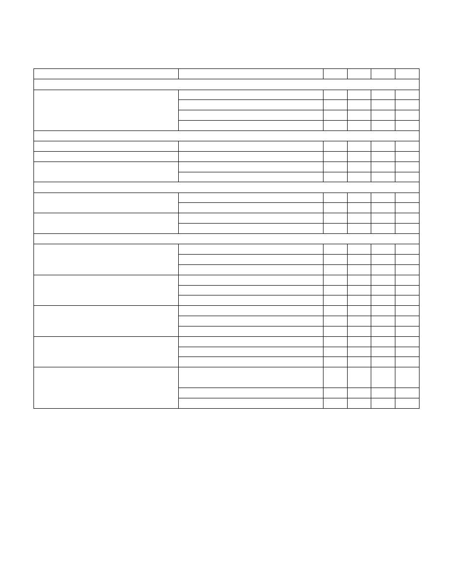
ELECTRICAL CHARACTERISTICS:
Unless otherwise stated, V
CC
= 15V. T
A
=T
J.
PARAMETER
TEST CONDITIONS
MIN
TYP
MAX
UNITS
Input Supply
Supply Current (Note 3)
Both inputs = 0V; V
CC
= 15V
11
15
mA
Both inputs = 5V; V
CC= 15V
20
27
mA
Both inputs = 0V; V
CC= 35V
15
20
mA
Both inputs = 5V; V
CC= 35V
41
56
mA
Logic Inputs
Logic 0 Input Voltage
0.8
V
Logic 1 Input Voltage
2.2
V
Input Current
V
IN
= 0V
-5.0
-2.7
mA
V
IN
= 5V
0.5
2.0
mA
Output Stages
Output High Level
I
SOURCE
= 20mA, below V
CC
1.5
2.0
V
I
SOURCE
= 200mA, below V
CC
2.0
3.0
V
Output Low Level
I
SINK
= 20mA
.25
0.4
V
I
SINK
= 200mA
0.4
1.0
V
Switching Characteristics (Note 4)
Rise Time Delay, TPLH
C
LOAD
= 0
10
40
ns
C
LOAD
= 1000pF, (Note 5)
15
50
ns
C
LOAD
= 2200pF
20
55
ns
Fall Time Delay, TPHL
C
LOAD
= 0
3
20
ns
C
LOAD
= 1000pf, (Note 5)
5
20
ns
C
LOAD
= 2200pF
5
20
ns
Rise Time, TLH
C
LOAD
= 0, (Note 5)
12
25
ns
C
LOAD
= 1000pF, (Note 5)
25
40
ns
C
LOAD
= 2200pF
40
55
ns
Fall Time, THL
C
LOAD
= 0, (Note 5)
7
15
ns
C
LOAD
= 1000pF, (Note 5)
25
40
ns
C
LOAD
= 2200pF
40
55
ns
Total Supply Current
Freq = 200kHz, 50% Duty-cycle
Both Channels Switching
C
LOAD
= 0
17
23
mA
C
LOAD
= 2200pF
29
35
mA
Note 3: Supply currents at other input supply votages can be calculated by extrapolating the 15V and 35V supply currents. The im-
pedance of the chip at the V
CC
pin is linear for supply voltages from 8V to 35V, the approximate value of this impedance is 4.3k for
both inputs low, 0.94k for both inputs high, and 1.54k for one input high and one low.
Note 4: Switching test conditions are, V
CC
= 15V, Input voltage waveform levels are 0V and 5V, with transition times of <3ns. The
timing terms are defined as : TPHL Propagation delay 50% V
IN
to 90% V
OUT
; TPLH Propogation delay 50% V
IN
to 10% V
OUT
; THL
90% V
OUT
to 10% V
OUT
; TLH 10% V
OUT
to 90% V
OUT
.
Note 5: This specification not tested in production.Unless otherwise stated specifications hold for T
A
= 0 to 70∞C for the UC3711,
and T
A
= -55 to 125∞C for the UC1711, V
CC
= 15V. T
A
= T
J
.
UNITRODE CORPORATION
7 CONTINENTAL BLVD. ∑ MERRIMACK, NH 03054
TEL. (603) 424-2410 FAX (603) 424-3460

IMPORTANT NOTICE
Texas Instruments and its subsidiaries (TI) reserve the right to make changes to their products or to discontinue
any product or service without notice, and advise customers to obtain the latest version of relevant information
to verify, before placing orders, that information being relied on is current and complete. All products are sold
subject to the terms and conditions of sale supplied at the time of order acknowledgement, including those
pertaining to warranty, patent infringement, and limitation of liability.
TI warrants performance of its semiconductor products to the specifications applicable at the time of sale in
accordance with TI's standard warranty. Testing and other quality control techniques are utilized to the extent
TI deems necessary to support this warranty. Specific testing of all parameters of each device is not necessarily
performed, except those mandated by government requirements.
CERTAIN APPLICATIONS USING SEMICONDUCTOR PRODUCTS MAY INVOLVE POTENTIAL RISKS OF
DEATH, PERSONAL INJURY, OR SEVERE PROPERTY OR ENVIRONMENTAL DAMAGE ("CRITICAL
APPLICATIONS"). TI SEMICONDUCTOR PRODUCTS ARE NOT DESIGNED, AUTHORIZED, OR
WARRANTED TO BE SUITABLE FOR USE IN LIFE-SUPPORT DEVICES OR SYSTEMS OR OTHER
CRITICAL APPLICATIONS. INCLUSION OF TI PRODUCTS IN SUCH APPLICATIONS IS UNDERSTOOD TO
BE FULLY AT THE CUSTOMER'S RISK.
In order to minimize risks associated with the customer's applications, adequate design and operating
safeguards must be provided by the customer to minimize inherent or procedural hazards.
TI assumes no liability for applications assistance or customer product design. TI does not warrant or represent
that any license, either express or implied, is granted under any patent right, copyright, mask work right, or other
intellectual property right of TI covering or relating to any combination, machine, or process in which such
semiconductor products or services might be or are used. TI's publication of information regarding any third
party's products or services does not constitute TI's approval, warranty or endorsement thereof.
Copyright
©
1999, Texas Instruments Incorporated