 | –≠–ª–µ–∫—Ç—Ä–æ–Ω–Ω—ã–π –∫–æ–º–ø–æ–Ω–µ–Ω—Ç: UC17132 | –°–∫–∞—á–∞—Ç—å:  PDF PDF  ZIP ZIP |
UC17131/2/3
UC27131/2/3
UC37131/2/3
SLUS340 - APRIL 1999
FEATURES
∑
300mA Continuous Output Current
∑
Low Side or High Side Switch
Configuration
∑
8V to 65V Operation
∑
Overload and Short Circuit Protection
∑
Power Interruption Protection
∑
+6V Regulated Voltage
∑
2mA Quiescent Current
∑
Programmable Overcurrent and
Power Interruption Protection
∑
1% to 30% Programmable Input
Comparator Hysteresis (on UC37132)
∑
Low and High Side Internal High
Current Clamps When Driving
Inductive Loads
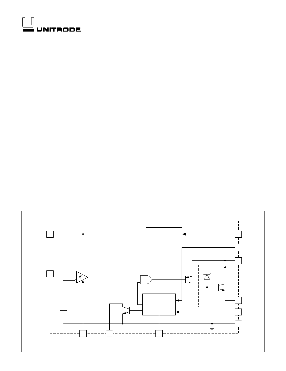
Smart Power Switch
13
12
11
VREF
IN
6
10
3
7
VCC
LS
CSH
CSL
2
GND
6V
PRE-REGULATOR
INPUT
COMPARATOR
1/2
VREF
HYST
9
LED
TURN-ON/OFF
AND
SHORT CIRCUIT
PROTECTION
4
HS
5
Q
OUT
72V
6V/8mA
CDEL
UC37132 BLOCK DIAGRAM
UDG-98026
DESCRIPTION
The UC37131, UC37132 and UC37133 are a family of smart power
switches which can drive resistive or inductive loads from the high side or
low side.
The UC37132 is available in 14 pin (DIP), 16 pin (SOIC), or 20 pin (CLCC)
packages and can accommodate both low side (load to VCC) or high side
(load to GND) configurations. The UC37131 and UC37133 are exclusively
for a low side or a high side configuration respectively and both are avail-
able in an 8 pin package. Both high side and low side configurations provide
high current switching with low saturation voltages which can drive resistive
or inductive loads.
The input to the switch is driven by a low voltage signal, typically 5V. Addi-
tionally, UC37132 features adjustable hysteresis. The output of the device
can switch a load between 8V and 65V. Output current capability is 300mA
continuous or 700mA peak.
The device also has inherent smart features that allow for programmable
turn-on delay in enabling the output following startup. The same capacitor
that specifies the turn-on delay is also used to program a VCC power inter-
ruption time. If VCC drops below a threshold for a time specified by this ca-
pacitor, the output is turned off and a new turn-on delay will be re-triggered.
Similarly, if high current persists longer than the response delay, the output
driver will operate in a very low duty cycle mode to protect the IC.
2
UC17131/2/3
UC27131/2/3
UC37131/2/3
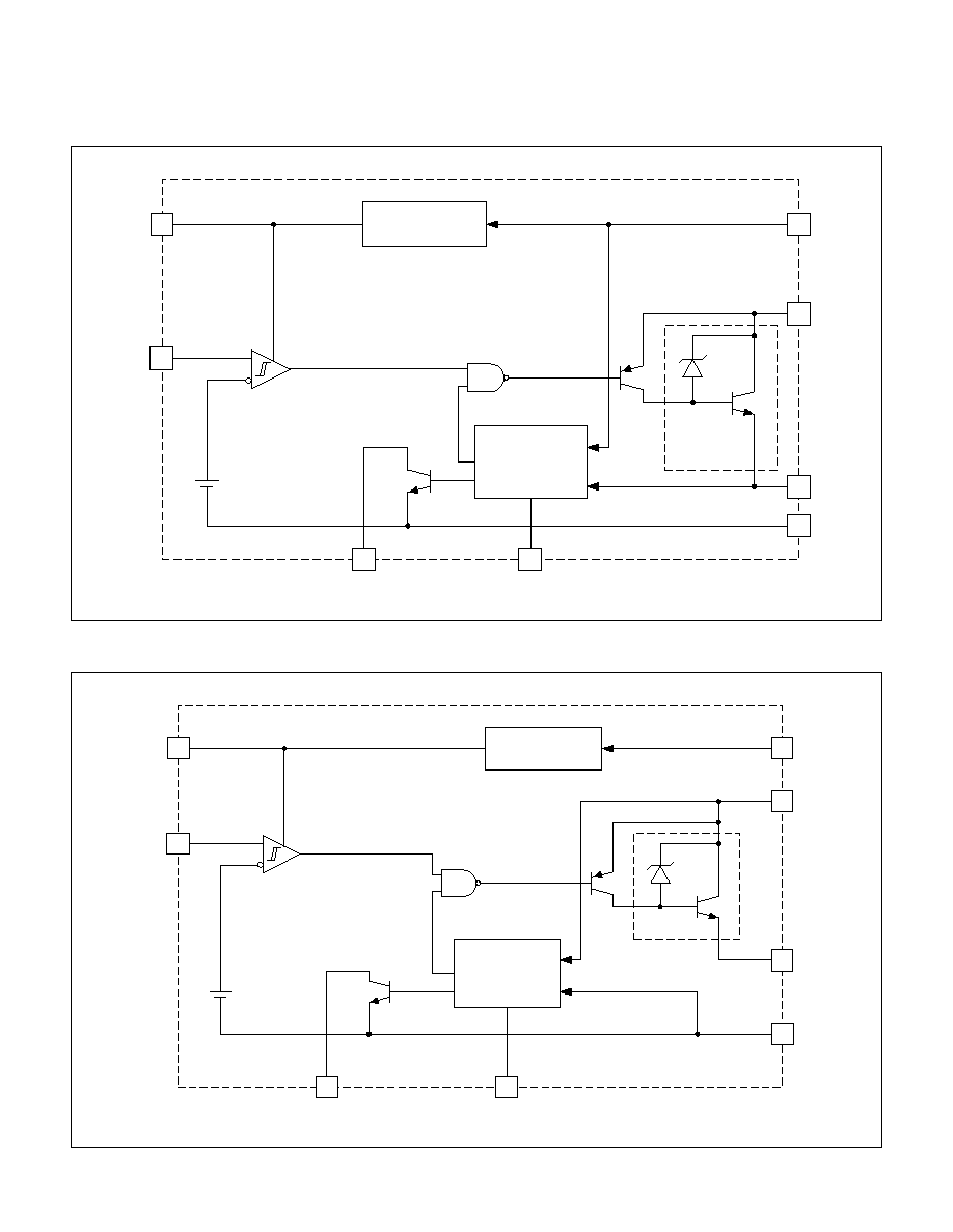
4
3
VREF
IN
2
6
8
VCC
LS
CSL
5
GND
6V
PRE-REGULATOR
INPUT
COMPARATOR
1/2
VREF
1
LED
TURN-ON/OFF
AND
SHORT CIRCUIT
PROTECTION
7
Q
OUT
72V
6V/8mA
CDEL
HYST (FIXED) =
30%
UC37131 BLOCK DIAGRAM
UDG-98059
4
3
VREF
IN
2
8
VCC
CSH
5
GND
6V
PRE-REGULATOR
INPUT
COMPARATOR
1/2
VREF
1
LED
TURN-ON/OFF
AND
SHORT CIRCUIT
PROTECTION
6
HS
7
Q
OUT
72V
6V/8mA
CDEL
HYST (FIXED) =
30%
UC37133 BLOCK DIAGRAM
UDG-98060

3
UC17131/2/3
UC27131/2/3
UC37131/2/3
HS
CSH
VCC
GND
1
2
3
4
8
7
6
5
CDEL
LED
VREF
IN
ABSOLUTE MAXIMUM RATINGS
VCC . . . . . . . . . . . . . . . . . . . . . . . . . . . . . . . . . . . . . . . . . . . 65V
LS ≠ HS (Clamped by internal circuitry) . . . . . . . . . . . . . . . 78V
CSH, LED . . . . . . . . . . . . . . . . . . . . . . . . . . . . . . . . . . . . . . 65V
Output Current
Continuous . . . . . . . . . . . . . . . . . . . . . . . . . . . . . . . . 400mA
Peak . . . . . . . . . . . . . . . . . . . . . . . . . . . . . . . . . . . . . 900mA
Remaining Pin Voltages . . . . . . . . . . . . . . . . . . . . . ≠0.3V to 9V
Storage Temperature . . . . . . . . . . . . . . . . . . .
-
65∞C to +150∞C
Junction Temperature . . . . . . . . . . . . . . . . . . . ≠55∞C to +150∞C
Lead Temperature (Soldering, 10 sec.) . . . . . . . . . . . . . +300∞C
Currents are positive into, negative out of the specified termi-
nal. Consult Packaging Section of Databook for thermal limita-
tions and considerations of packages.
PART
NUMBER
CONFIGURATIONS
PACKAGE
PIN COUNT
UCX7131
Low Side Only
8
UCX7132
Low Side or High Side
14, 16, 20
UCX7133
High Side Only
8
PRODUCT SELECTION TABLES
PART
NUMBER
TEMPERATURE
RANGE
AVAILABLE
PACKAGES
UC1713X
≠55∞C to +125∞C
J, L
UC2713X
≠40∞C to +85∞C
D, N
UC3713X
0∞C to +70∞C
D, N
HYST
IN
N/C
VREF
CDEL
N/C
LED
1
2
3
4
5
6
7
14
13
12
11
10
9
8
GND
N/C
CSH
VCC
CSL
HS
LS
CSL
LS
VCC
GND
1
2
3
4
8
7
6
5
CDEL
LED
VREF
IN
HYST
IN
N/C
VREF
CDEL
N/C
LED
N/C
1
2
3
4
5
6
7
8
16
15
14
13
12
11
10
9
GND
N/C
VCC
CSH
N/C
CSL
HS
LS
CONNECTION DIAGRAMS
SOIC-16 (Top View)
(for UCX7132)
D Package
3
18
17
16
N/C
1
2
20 19
15
14
4
5
6
7
8
9
11
10
12 13
LS
CSH
HS
CSL
N/C
GND
N/C
N/C
IN
N/C
VCC
N/C
N/C
N/C
HYST
VREF
CDEL
N/C
LED
PLCC-20 (Top View)
(for UCX7132)
L Packages
DIL-14 (Top View)
(for UCX7132)
J, or N Packages
DIL-8, SOIC-8 (Top View)
(for UCX7131)
J, N, or D Packages
DIL-8, SOIC-8 (Top View)
(for UCX7133)
J, N, or D Packages

4
UC17131/2/3
UC27131/2/3
UC37131/2/3
ELECTRICAL CHARACTERISTICS
Unless otherwise specified, CDEL = 10nF, VCC = 25V, CSL = GND, CSH = LS;
R
CSH
= 0.5
(Note 1); IN=0V (for OFF condition) and IN=5V (for ON condition); T
A
= T
J
.
PARAMETER
TEST CONDITIONS
MIN
TYP
MAX
UNITS
Reference
VREF
25∞C
5.8
6
6.2
V
≠55∞C to 125∞C
5.6
6
6.4
V
Line Regulation
VCC = 8V to 64V
10
35
mV
Load Regulation
0 < I
REF
< 8mA
10
50
mV
Short Circuit Current
REF = 0V
20
35
mA
Input Comparator
Turn-On Threshold Voltage
2.7
3
3.3
V
Input Bias Current
V
IN
= 3.5V
5
µ
A
Hysteresis
R
HYST
= GND (Internally for X31, X33)
0.775
0.9
1.025
V
R
HYST
= 96.67k for (X32)
30
mV
Output: High Side (UCX7133: CSH = LS and CSL = GND Internally; See Fig. 2a)
Rise Time (Off to On)
R
LOAD
= 250
to GND
30
80
V/
µ
s
Fall Time (On to Off)
R
LOAD
= 250
to GND
30
80
V/
µ
s
Output Short Circuit
HS = 0.25
to GND
500
900
mA
Voltage Clamp
LS≠HS
67
72
77
V
Saturation Voltage
25∞C, R
LOAD
= 100
to GND
1.2
V
≠40∞C, R
LOAD
= 100
to GND
1.3
V
≠55∞C, R
LOAD
= 100
to GND
1.4
V
Leakage Current
5
µ
A
Output: Low Side (UCX7131; CSH = VCC and CSL = HS Internally; See Fig. 2b)
Rise Time (On to Off)
R
LOAD
= 250
to VCC, R
CSL
= 0.5
15
50
V/
µ
s
Fall Time (Off to On)
R
LOAD
= 250
to VCC, R
CSL
= 0.5
25
60
V/
µ
s
Output Short Circuit
LS = 0.25
to VCC
500
700
900
mA
Voltage Clamp
LS≠HS
67
72
77
V
Saturation Voltage
25∞C, R
LOAD
= 100
to VCC, R
CSL
= 0.5
1.2
V
≠40∞C, R
LOAD
= 100
to VCC, R
CSL
= 0.5
1.3
V
≠55∞C, R
LOAD
= 100
to VCC, R
CSL
= 0.5
1.4
V
Leakage Current
5
µ
A
VCC Fault Section
Output Turn-On Delay, t
D(ON)
Step VCC from 0V to 8V (See Fig. 3a)
9.5
11
13.5
ms
Output Turn-Off Delay, t
D(OFF)
Pulse VCC from 25V to VCC Turn-Off
Threshold
300
500
700
µ
s
VCC Turn-Off Threshold
Pulse VCC Low
6.5
7
7.5
V
CDEL Section
V
CDEL_MAX
5.8
V
V
FAULT_H
4.9
V
V
FAULT_L
1.0
V
Overcurrent Fault Section (See Fig. 3c)
Short Circuit Turn-Off Delay, t
SC
Step I
LOAD:
0mA to 400mA
75
µ
s
Short Circuit Recovery Time, t
ROFF
I
LOAD
= 400mA, 100
µ
s
10
ms
High Side Current Threshold, I
TH-H
R
CSH
= 0.5
250
325
400
mA
Low Side Current Threshold, I
TH-L
R
CSL
= 0.5
250
325
400
mA
Overcurrent Duty Cycle
R
LOAD
= 0.25
to GND
0.6
0.8
1.0
%

5
UC17131/2/3
UC27131/2/3
UC37131/2/3
ELECTRICAL CHARACTERISTICS
Unless otherwise specified, CDEL = 10nF, VCC = 25V, CSL = GND, CSH = LS;
R
CSH
= 0.5
(Note 1); IN=0V (for OFF condition) and IN=5V (for ON condition); T
A
= T
J
.
PARAMETER
TEST CONDITIONS
MIN
TYP
MAX
UNITS
LED Output
I
SINK
, t
DOFF
, t
ROFF
V
LED
= 7V
5.0
8.0
11.0
mA
I
LEAKAGE
1
5
µ
A
Overall
Delay to Output
3
6
µ
s
ICC
Output Off
2.0
2.8
mA
I
L
= 1mA, 250mA (High Side)
2.3
3
mA
I
L
= 1mA, 250mA (Low Side)
2.5
4
mA
Note 1: All test conditions are for a high side configuration as in Fig. 2a, unless otherwise specified.
CDEL: A capacitor connected to this pin is used to pro-
gram both VCC pulse interruption time and power
turn-on delay. The capacitor discharge time corresponds
to VCC interruption and the charge time to VCC turn-on
delay. The ratio between turn-on delay and turn-off delay
will be fixed based on internal charge and discharge cur-
rents and voltage thresholds.
The same fault circuitry and capacitor is used for short
circuit and overload protection. If an overcurrent or short
circuit is detected, the capacitor starts charging and
turns off the output if the condition persists at the end of
its charge time. The output will then operate in a low-duty
cycle mode to protect the IC. After short circuit recovery,
the output will be reactivated in order to check if the short
circuit was removed. If the overcurrent persists the chip
will continue in this pulsing mode.
CSH: (For UC37132 and UC37133) This high side cur-
rent sense pin is used to program the current limit for
high side applications by connecting a resistor between
VCC and CSH. An over load current is detected when
the voltage drop between VCC and CSH exceeds
150mV. For the UC37132, in a high side application, the
CSH pin must be tied to the LS pin; in a low side applica-
tion, the CSH pin must be tied to VCC
CSL: (For UC37131 and UC37132) This low side cur-
rent sense pin is used to program the current limit for low
side applications by connecting a resistor between CSL
and GND. An over load current is detected when the volt-
age drop between CSL and GND exceeds 150mV. For
the UC37132, in a high side application, the CSL pin
must be tied to GND; in a low side application, the CSL
pin must be tied to the HS pin.
GND: The reference point for the internal reference, all
thresholds, and the return for the remainder of the de-
vice.
HS: (For UC37132 and UC37133) The output of the
switching transistor in the high side configuration. The
emitter of the output transistor is the HS pin which is con-
nected to the load. For the UC37132, the HS pin must be
tied to the CSL pin in a low side application.
HYST: (For UC37132) The pin used to program the in-
put comparator hysteresis by connecting a resistor to
ground. The hysteresis defaults to 30% with HYST
grounded (internally for UC37131 and UC37133).
V
R
HYST
HYST
=
+
3000
3330
(
)
IN: The input to the comparator that detects when the
output transistor should be turned on. The input thresh-
old is 3.0V (1/2 VREF) and the input voltage range is 0V
to VREF.
LED: Open collector output intended to drive an LED.
This pin is driven low whenever the output is turned off
and is externally pulled high when the output is turned on
(see Fig. 3b and 3c).
LS: (For UC37131 and UC37132) The output of the
switching transistor in the low side configuration. The col-
lector of the output transistor is the LS pin which is con-
nected to the load. For the UC37132, the LS pin must be
tied to the CSH pin in a high side application.
VREF: The 6V regulated reference capable of supplying
up to 8mA. The recommended decoupling capacitor is
1nF.
VCC: The supply voltage for the chip. Decouple this pin
with a good quality ceramic capacitor to ground.
PIN DESCRIPTIONS