Document Outline
- Application Notes
- Design Notes
1/94
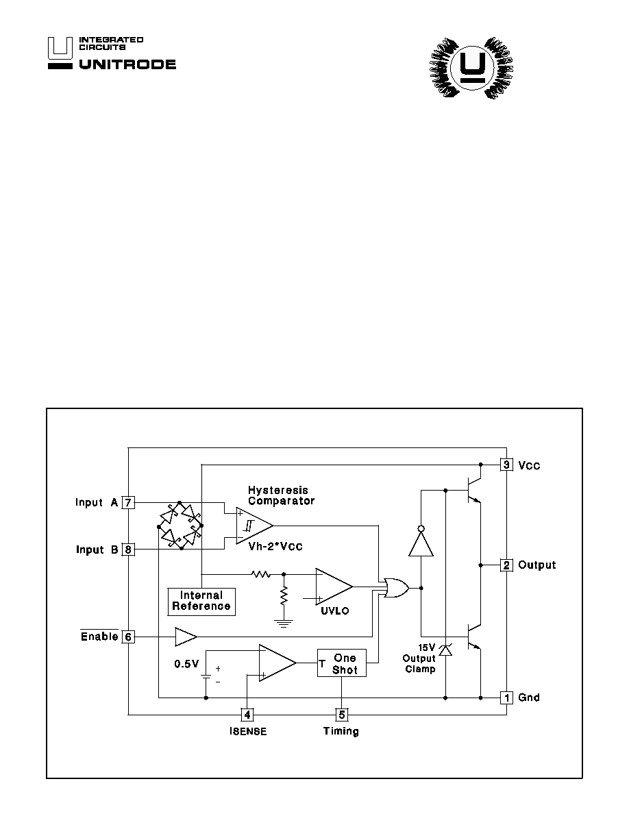
BLOCK DIAGRAM
∑
Receives Both Power and Signal Across
the Isolation Boundary
∑
9 to 15 Volt High Level Gate Drive
∑
Under-voltage Lockout
∑
Programmable Over-current Shutdown
and Restart
∑
Output Enable Function
The UC1725 and its companion chip, the UC1724, provide all the nec-
essary features to drive an isolated MOSFET transistor from a TTL in-
put signal. A unique modulation scheme is used to transmit both power
and signals across an isolation boundary with a minimum of external
components.
Protection circuitry, including under-voltage lockout, over-current shut-
down, and gate voltage clamping provide fault protection for the MOS-
FET. High level gate drive is guaranteed to be greater than 9 volts and
less than 15 volts under all conditions.
Uses include isolated off-line full bridge and half bridge drives for driv-
ing motors, switches, and any other load requiring full electrical isola-
tion.
The UC1725 is characterized for operation over the full military tem-
perature range of -55∞C to +125∞C while the UC2725 and UC3725 are
characterized for -25∞C to +85∞C and 0∞C to +70∞C respectively.
UC1725
UC2725
UC3725
Isolated High Side FET Driver
FEATURES
DESCRIPTION
UDG-92051-1
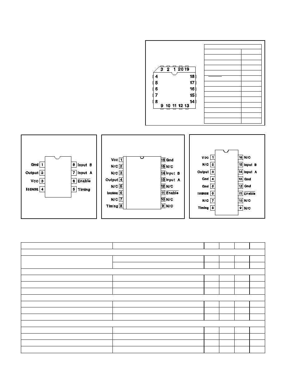
CONNECTION DIAGRAMS
DIL-8 (Top View)
J Or N Package
UC1725
UC2725
UC3725
PACKAGE PIN FUNCTION
FUNCTION
PIN
N/C
1
I
SENSE
2
N/C
3-5
Timing
6
Enable
7
N/C
8-9
Input A
11
N/C
12-14
Input B
15
Gnd
16
V
CC
17
N/C
18-19
Output
20
PLCC-20 (Top View)
Q Package
ABSOLUTE MAXIMUM RATINGS
Supply Voltage (pin 3) . . . . . . . . . . . . . . . . . . . . . . . . . . . . . 30V
Power inputs (pins 7 & 8) . . . . . . . . . . . . . . . . . . . . . . . . . . . 30V
Output current, source or sink (pin 2)
DC. . . . . . . . . . . . . . . . . . . . . . . . . . . . . . . . . . . . . . . . . . . . 0.5A
Pulse (0.5 us) . . . . . . . . . . . . . . . . . . . . . . . . . . . . . . . . . . . 2.0A
Enable and Current limit inputs (pins 4 & 6). . . . . . . . -0.3 to 6V
Power Dissipation at T
A
25∞C (DIL-8) . . . . . . . . . . . . . . . . 1W
Power Dissipation at T
A
25∞C (SO-14) . . . . . . . . . . . . 725mW
Lead Temperature (Soldering, 10 Seconds) . . . . . . . . . . 300∞C
Note 1: Unless otherwise indicated, voltages are referenced to
ground and currents are positive into, negative out of, the speci-
fied terminals (pin numbers refer to DIL-8 package).
Note 2: See Unitrode Integrated Circuits databook for
information regarding thermal specifications and limitations of
packages.
PARAMETER
TEST CONDITIONS
MIN
TYP
MAX UNITS
POWER INPUT SECTION (PINS 7 & 8)
Forward Diode Drop, Schottky Rectifier
I
F
= 50ma
.55
.7
V
I
F
= 500ma
1.1
1.5
V
CURRENT LIMIT SECTION (PIN 4)
Input bias current
V
PIN4
= OV
-1
-10
µ
A
Threshold voltage
0.4
0.5
0.6
V
Delay to outputs
V
PIN4
= 0 to 1V
100
250
ns
TIMING SECTION (PIN 5)
Output Off Time
27
30
33
µ
s
Upper Mono Threshold
6.3
7.0
7.7
V
Lower Mono Threshold
1.9
2.0
2.3
V
HYSTERESIS AMPLIFIER (PINS 7 & 8)
Input Open Circuit Voltage
Inputs (pins 7 & 8), Open Circuited, T
A
= 25∞C
7.0
Vcc/2
8.0
V
Input Impedance
T
A
= 25∞C
23
28
33
k
Hysteresis
26.5
2*Vcc
30.5
V
Delay to Outputs
V
PIN7
- V
PIN8
= V
CC
+ 1V
100
300
ns
ELECTRICAL CHARACTERISTICS:
(Unless otherwise stated, these specifications apply for -55
∞
C
T
A
+125
∞
C for
UC1725; -25
∞
C
T
A
+85
∞
C for UC2725; 0
∞
C
T
A
+70
∞
C for UC3725; V
CC
(pin 3) =
0 to 15V, R
T
=10k, C
T
=2.2nf, T
A
=T
J
, pin numbers refer to DIL-8 package.)
SOIC-16 (Top View)
DW Package
DIL-16 (Top View)
JE Or NE Package
2
PARAMETER
TEST CONDITIONS
MIN
TYP
MAX UNITS
ENABLE SECTION (PIN 6)
High Level Input Voltage
2.1
1.4
V
Low Level Input Voltage
1.4
.8
V
Input Bias Current
-250
-500
µ
A
OUTPUT SECTION
Output Low Level
I
OUT
= 20mA
0.35
0.5
V
I
OUT
= 200mA
0.6
2.5
V
Output High Level
I
OUT
= -20mA
13
13.5
V
I
OUT
= -200mA
12
13.4
V
V
CC
= 30V, Iout = -20mA
14
15
V
Rise/Fall Time
C
T
= 1nf
30
60
ns
UNDER VOLTAGE LOCKOUT
UVLO Low Saturation
20mA, V
CC
= 8V
0.8
1.5
V
Start-up Threshold
11.2
12
12.6
V
Threshold Hysteresis
.75
1.0
1.12
V
TOTAL STANDBY CURRENT
Supply Current
12
16
ma
UC1725
UC2725
UC3725
ELECTRICAL
CHARACTERISTICS (cont.)
(Unless otherwise stated, these specifications apply for -55
∞
C
T
A
+125
∞
C for UC1725;
-25
∞
C
T
A
+85
∞
C for UC2725; 0
∞
C
T
A
+70
∞
C for UC3725; V
CC
(pin 3) = 0 to 15V, Rt=10k,
C
T
=2.2nf, T
A
=T
J,
pin numbers refer to DIL-8 package.)
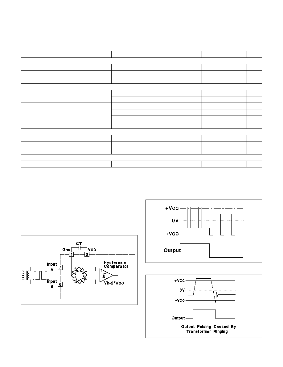
INPUTS: Figure 1 shows the rectification and detection
scheme used in the UC1725 to derive both power and
signal information from the input waveform. Vcc is gener-
ated by peak detecting the input signal via the internal
bridge rectifier and storing on a small external capacitor,
C1. Note that this capacitor is also used to bypass high
pulse currents in the output stage, and therefore should
be placed direclty between pins 1 and 3 using minimal
lead lengths.
Signal detection is performed by the internal hysteresis
comparator which senses the polarity of the input signal
as shown in Figure 2. This is accomplished by setting
(resetting) the comparator only if the input signal ex-
ceeds Vcc (-Vcc). In some cases it may be necessary to
add a damping resistor across the transformer secondary
to minimize ringing and eliminate false triggering of the
hysteresis amplifier as shown in Figure 3.
APPLICATION AND OPERATION INFORMATION
FIGURE 1 - Input Stage
FIGURE 2 - Input Waveform (DIL-8 Pin 7 - Pin 8)
FIGURE 3 - Signal Detection
UDG-92047
UDG-92048
UDG-92049
3
UC1725
UC2725
UC3725
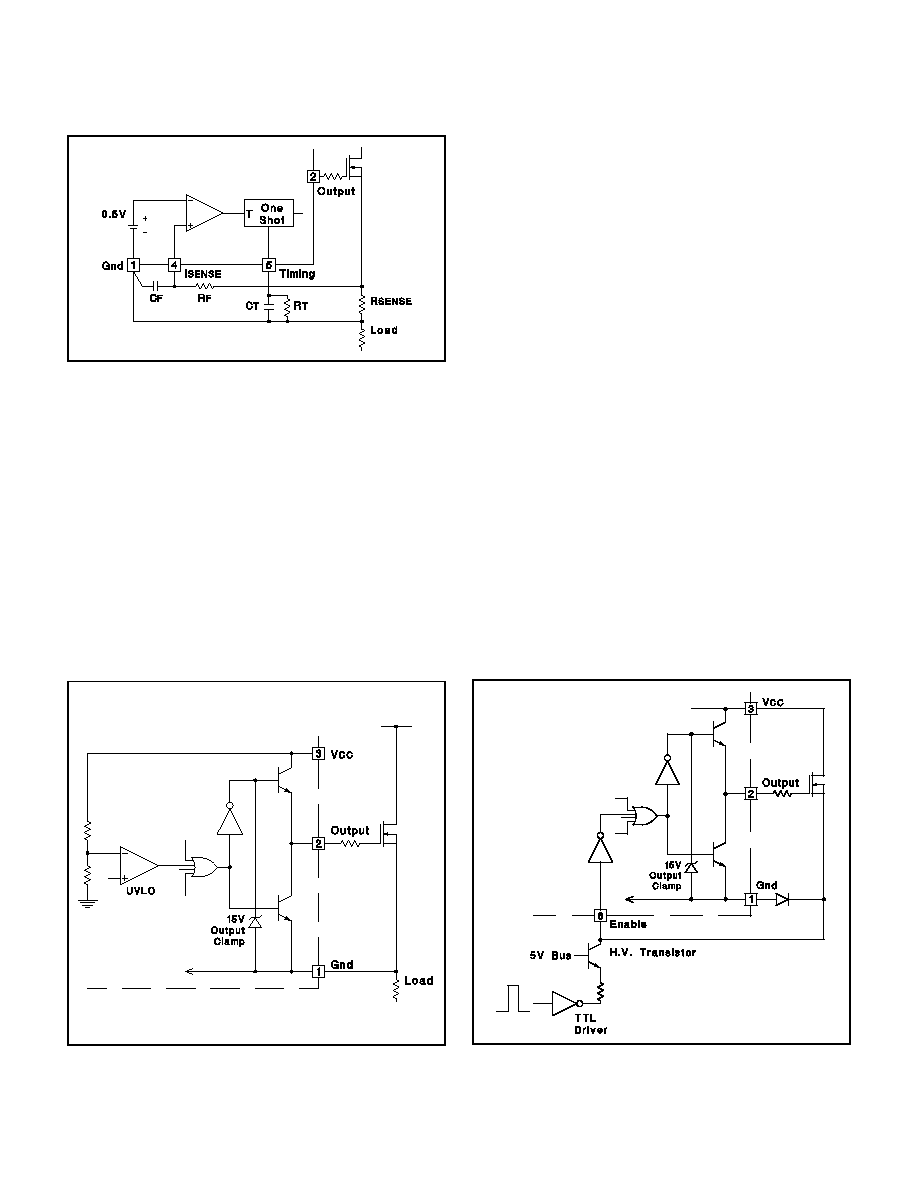
CURRENT LIMIT AND TIMING: Current sensing and
shutdown can be implemented directly at the output us-
ing the scheme shown in Figure 4. Alternatively, a current
transformer can be used in place of R
SENSE
. A small RC
filter in series with the input (pin 4) is generally needed to
eliminate the leading edge current spike caused by
parasitic circuit capacitances being charged during turn
on. Due to the speed of the current sense circuit, it is
very important to ground C
F
directly to Gnd as shown to
eliminate false triggering of the one shot caused by
ground drops.
One shot timing is easily programmed using an external
capacitor and resistor as shown in Figure 4. This, in turn,
controls the output off time according to the formula:
T
OFF
= 1.28
∑
RC.
If current limit feature is not required, simply ground pin 4
and leave pin 5 open.
OUTPUT: Gate drive to the power FET is provided by a
totem pole output stage capable of sourcing and sinking
currents in excess of 1 amp. The undervoltage lockout
circuit guarantees that the high level output will never be
less than 9 volts. In addition, during undervoltage lock-
out, the output stage will actively sink current to eliminate
the need for an external gate to source resistor. High
level output is also clamped to 15 volts. Under high ca-
pacitive loading however, the output may overshoot 2 to
3 volts, due to the drivers' inabitlity to switch from full to
zero output current instantaneously. In a practical circuit
this is not normally a concern. A few ohms of series gate
resistance is normally required to prevent parasitic oscil-
lations, and will also eliminate overshoot at the gate.
ENABLE: An enable pin is provided as a fast, digital in-
put that can be used in a number of applications to di-
rectly switch the output. Figure 6 shows a simple means
of providing a fast, high voltage translation by using a
small signal, high voltage transistor in a cascode configu-
ration. Note that the UC1725 is still used to provide
power, drive and protection circuitry for the power FET.
FIGURE 4 - Current Limit
UDG-92050
FIGURE 5 - Output Circuit
FIGURE 6 - Using Enable Pin as a High Speed Input
Path
UDG-92052
UDG-92053
UNITRODE INTEGRATED CIRCUITS
7 CONTINENTAL BLVD.
∑
MERRIMACK, NH 03054
TEL. (603) 424-2410
∑
FAX (603) 424-3460
4

IMPORTANT NOTICE
Texas Instruments and its subsidiaries (TI) reserve the right to make changes to their products or to discontinue
any product or service without notice, and advise customers to obtain the latest version of relevant information
to verify, before placing orders, that information being relied on is current and complete. All products are sold
subject to the terms and conditions of sale supplied at the time of order acknowledgement, including those
pertaining to warranty, patent infringement, and limitation of liability.
TI warrants performance of its semiconductor products to the specifications applicable at the time of sale in
accordance with TI's standard warranty. Testing and other quality control techniques are utilized to the extent
TI deems necessary to support this warranty. Specific testing of all parameters of each device is not necessarily
performed, except those mandated by government requirements.
CERTAIN APPLICATIONS USING SEMICONDUCTOR PRODUCTS MAY INVOLVE POTENTIAL RISKS OF
DEATH, PERSONAL INJURY, OR SEVERE PROPERTY OR ENVIRONMENTAL DAMAGE ("CRITICAL
APPLICATIONS"). TI SEMICONDUCTOR PRODUCTS ARE NOT DESIGNED, AUTHORIZED, OR
WARRANTED TO BE SUITABLE FOR USE IN LIFE-SUPPORT DEVICES OR SYSTEMS OR OTHER
CRITICAL APPLICATIONS. INCLUSION OF TI PRODUCTS IN SUCH APPLICATIONS IS UNDERSTOOD TO
BE FULLY AT THE CUSTOMER'S RISK.
In order to minimize risks associated with the customer's applications, adequate design and operating
safeguards must be provided by the customer to minimize inherent or procedural hazards.
TI assumes no liability for applications assistance or customer product design. TI does not warrant or represent
that any license, either express or implied, is granted under any patent right, copyright, mask work right, or other
intellectual property right of TI covering or relating to any combination, machine, or process in which such
semiconductor products or services might be or are used. TI's publication of information regarding any third
party's products or services does not constitute TI's approval, warranty or endorsement thereof.
Copyright
©
1999, Texas Instruments Incorporated