 | –≠–ª–µ–∫—Ç—Ä–æ–Ω–Ω—ã–π –∫–æ–º–ø–æ–Ω–µ–Ω—Ç: UC1730 | –°–∫–∞—á–∞—Ç—å:  PDF PDF  ZIP ZIP |
Thermal Monitor
UC1730
UC2730
UC3730
DESCRIPTION
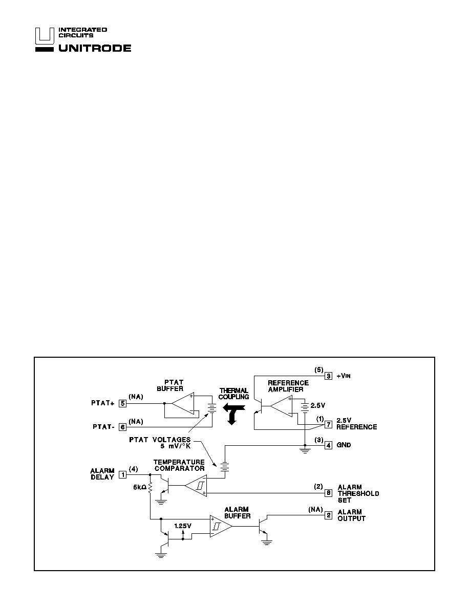
The UC1730 family of integrated circuit devices are designed to be used in
a number of thermal monitoring applications. Each IC combines a tempera-
ture transducer, precision reference, and temperature comparator allowing
the device to respond with a logic output if temperatures exceed a user pro-
grammed level. The reference on these devices is capable of supplying in
excess of 250mA of output current
-
by setting a level of power dissipation
the rise in die temperature will vary with airflow past the package, allowing
the IC to respond to airflow conditions
These devices come in an 8-Pin DIP, plastic or ceramic, a 5-Pin TO-220 or a
PLCC-20 version. In the 8-Pin version, a PTAT (proportional to absolute
temperature) output reports die temperature directly. This output is config-
ured such that its output level can be easily scaled up with two external gain
resistors. A second PTAT source is internally referenced to the temperature
comparator. The other input to this comparator can then be externally pro-
grammed to set a temperature threshold. When this temperature threshold
is exceeded an alarm delay output is activated. Following the activation of
the delay output, a separate open collector output is turned on. The delay
pin can be programmed with an external RC to provide a time separation
between activation of the delay pin and the alarm pin, permitting shutdown
diagnostics in applications where the open collector outputs of multiple parts
are wire OR'ed together.
The 5-Pin version in the TO-220 package is well suited for monitoring
heatsink temperatures. Enhanced airflow sensitivities can be obtained with
this package by mounting the device to a small heatsink in the airstream.
This version of the device does not include the PTAT output or the open col-
lector alarm output.
FEATURES
∑
On-Chip Temperature Transducer
∑
Temperature Comparator Gives
Threshold Temperature Alarm
∑
Power Reference Permits Airflow
Diagnostics
∑
Precision 2.5V Power Reference
Permits Airflow Diagnostics
∑
Transducer Output is Easily Scaled
for Increased Sensitivity
∑
Low 2.5mA Quiescent Current
BLOCK DIAGRAM
10/94
Pin numbers shown for 8-Pin DIP, ( ) number for 5-Pin TO-220.
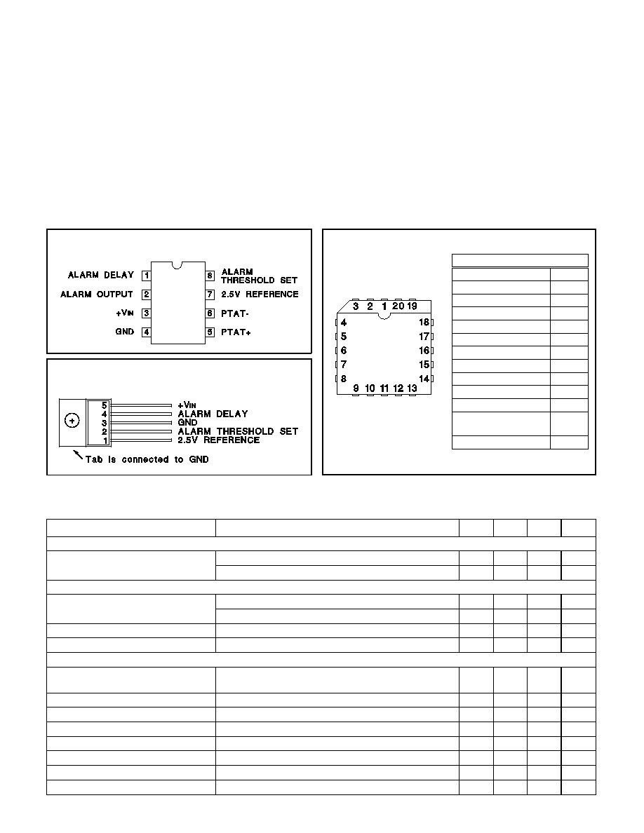
PACKAGE PIN FUNCTION
FUNCTION
PIN
N/C
1-3
ALARM DELAY
4
ALARM OUTPUT
5
+V
IN
6
GND
7
N/C
8-13
PTAT+
14
PTAT-
15
2.5V REFERENCE
16
2.5V REFERENCE
17
ALARM
THRESHOLD SET
18
N/C
19-20
Input Supply Voltage, (+V
IN
). . . . . . . . . . . . . . . . . . . . . . . 40V
Alarm Output Voltage (8-Pin Version Only) . . . . . . . . . . . 40V
Alarm Delay Voltage. . . . . . . . . . . . . . . . . . . . . . . . . . . . . 10V
Alarm Threshold Set Voltage . . . . . . . . . . . . . . . . . . . . . . 10V
2.5V Reference Output Current . . . . . . . . . . . . . . . . . -400 mA
Alarm Output Current (8-Pin Version Only) . . . . . . . . . . 0 mA
Power Dissipation at T
A
= 25∞C (Note 2) . . . . . . . . . 1000 mW
Power Dissipation at T
C
= 25∞C (Note 2) . . . . . . . . . 2000 mW
Thermal Resistance Junction to Ambient
N, 8-Pin Plastic DIP . . . . . . . . . . . . . . . . . . . . . . . . . 110∞C/W
J, 8-Pin Ceramic DIP . . . . . . . . . . . . . . . . . . . . . . . . 110∞C/W
T, 5-Pin Plastic DIP TO-220 . . . . . . . . . . . . . . . . . . . . 65∞C/W
Thermal Resistance Junction to Case
N, 8-Pin Plastic DIP . . . . . . . . . . . . . . . . . . . . . . . . . . . 60∞C/W
J, 8-Pin Ceramic DIP . . . . . . . . . . . . . . . . . . . . . . . . . . 40∞C/W
T, 5-Pin Plastic TO-220 . . . . . . . . . . . . . . . . . . . . . . . . . 5∞C/W
Operating Junction Temperature . . . . . . . . . -55∞C to +150∞C
Storage Temperature . . . . . . . . . . . . . . . . . . -65∞C to +150∞C
Lead Temperature (Soldering, 10 Seconds). . . . . . . . . 300∞C
Note 1: Voltages are referenced to ground. Currents are posi-
tive into, negative out of, the specified terminals.
Note 2: Consult Packaging section of Databook for thermal
limitations and considerations of package.
DIL-8 (TOP VIEW)
N or J Package
5-PIN TO-220 (TOP VIEW)
T Package
UC1730
UC2730
UC3730
CONNECTION DIAGRAMS
PLCC-20 (TOP VIEW)
Q Package
ABSOLUTE MAXIMUM RATINGS
ELECTRICAL CHARACTERISTICS:
PARAMETERS
TEST CONDITIONS
MIN
TYP
MAX
UNITS
INPUT SUPPLY
Supply Current
+V
IN
= 35V
2.8
4.0
mA
+V
IN
= 5V
2.3
3.5
mA
REFERENCE
Output Voltage
T
J
= 25∞C
2.475
2.5
2.525
V
Over Temperature
2.46
2.54
V
Load Regulation
I
OUT
= 0 to 250mA
8.0
25
mV
Line Regulation
+V
IN
= 5 to 25V
1.0
5.0
mV
TEMPERATURE COMPARATOR
Temperature Comparator Threshold at 300∞K (26.85∞C), Nominally 5mV/∞K,
V
INPUT
High to Low
1.475
1.50
1.525
V
Temperature Error
-10
10
∞C
Threshold Line Regulation
+V
IN
= 5 to 25V
0.005
0.02
%/V
Temperature Linearity
Note 2
2.0
5.0
∞C
Threshold Hysteresis
3.0
8.0
15
mV
Input Bias Current
V
INPUT
at 1.5V
-0.5
-0.1
µ
A
Max Output Current
V
OUT
= 1V
1.2
3.0
mA
Output Sat Voltage
I
OUT
= 100
µ
A
0.05
0.25
V
Unless otherwise stated, these specifications apply for T
J
= 0∞C to +100∞C for the
UC3730, -25∞C to + 100∞C for the UC2730 and -55∞C to +125∞C for the UC1730,
+V
IN
= + 5V, and PTAT≠ = 0V. T
A
= T
J
.
2

ELECTRICAL
CHARACTERISTICS (cont):
PARAMETERS
TEST CONDITIONS
MIN
TYP
MAX
UNIT
TEMPERATURE COMPARATOR (cont.)
Output Leakage Current
V
OUT
= 1V
0.01
1.0
µ
A
PTAT BUFFER (8-Pin N, or J Version Only)
Output Voltage
at 300∞K (26.85∞C), Nominally 5mV/∞K
1.460
1.50
1.54
V
In 10X Config. + V
IN
= 25V
14.6
15
15.4
V
Temperature Error
-12
12
∞C
Temperature Linearity (Note 2)
2.0
5.0
∞C
Line Regulation
+V
IN
= 5 to 25V
0.02
0.04
%/V
Load Regulation
I
OUT
= 0 to 2mA
1.0
3.0
mV
Dropout Voltage
PTAT + TO +V
IN
1.9
2.5
V
Input Bias Current at PTAT≠ Input
-3.0
-1.0
µ
A
ALARM BUFFER COMPARATOR (8-Pin N, or J Version Only)
Threshold Voltage (V
TH
)
Alarm Delay Input Low to High
1.1
1.2
1.3
V
Threshold Hysteresis Voltage
Alarm Delay Voltage > V
TH
100
250
mV
Input Bias Current
Alarm Delay Voltage < V
TH
0.1
0.5
µ
A
Max Output Current
V
OUT
= 1V
7.0
15
mA
Output Sat Voltage
I
OUT
= 3mA
0.25
0.45
V
Output Leakage
V
OUT
= 35V
0.1
2.0
µ
A
UC1730
UC2730
UC3730
Unless otherwise stated, these specifications apply for T
J
= 0∞C to +100∞C for the UC3730,
-25∞C to + 100∞C for the UC2730 and -55∞C to +125∞C for the UC1730, +V
IN
= + 5V, and
PTAT≠ = 0V. T
A
= T
J
.
Note 2: This parameter is guaranteed by design and is not tested in production.
APPLICATIONS AND OPERATION INFORMATION
V
OUT
=
5 x
1
+
R2
R1
mV
/
∞
K
(Recommended Range for R1 is 2k to 4k)
Scaling the PTAT Output (8 Pin Version Only)
V
REF
Maximum Output Current vs Input Supply
Junction Temperature Rise vs Airflow UC3730N (8-
Pin Plastic Dip)
3

Temperature Threshold (∞C)
=
(
2.5V
0.005
)
x
R2
R1
+
R2
-
273.15
Note:For airflow monitoring a power dissipation
level can be set with a resistive load, R
L
, on the
reference output. P
D
= (+ V
IN
- 2.5V)
2
/R
L
.
APPLICATIONS AND OPERATION INFORMATION (Cont.)
UC1730
UC2730
UC3730
Setting a Temperature Threshold
Dual Speed Fan Control
TH(∞C) =
2.5V
0.005
x
R2
R1
+
R2
-
273.15
TL(∞C) =
2.5V
0.005
x
R
X
R1
+
R
X
-
273.15
Where: RX = R2
◊
R3
R2
+
R3
UNITRODE INTEGRATED CIRCUITS
7 CONTINENTAL BLVD.
∑
∑
MERRIMACK, NH 03054
TEL. (603) 424-2410
∑
∑
FAX (603) 424-3460
4

IMPORTANT NOTICE
Texas Instruments and its subsidiaries (TI) reserve the right to make changes to their products or to discontinue
any product or service without notice, and advise customers to obtain the latest version of relevant information
to verify, before placing orders, that information being relied on is current and complete. All products are sold
subject to the terms and conditions of sale supplied at the time of order acknowledgement, including those
pertaining to warranty, patent infringement, and limitation of liability.
TI warrants performance of its semiconductor products to the specifications applicable at the time of sale in
accordance with TI's standard warranty. Testing and other quality control techniques are utilized to the extent
TI deems necessary to support this warranty. Specific testing of all parameters of each device is not necessarily
performed, except those mandated by government requirements.
CERTAIN APPLICATIONS USING SEMICONDUCTOR PRODUCTS MAY INVOLVE POTENTIAL RISKS OF
DEATH, PERSONAL INJURY, OR SEVERE PROPERTY OR ENVIRONMENTAL DAMAGE ("CRITICAL
APPLICATIONS"). TI SEMICONDUCTOR PRODUCTS ARE NOT DESIGNED, AUTHORIZED, OR
WARRANTED TO BE SUITABLE FOR USE IN LIFE-SUPPORT DEVICES OR SYSTEMS OR OTHER
CRITICAL APPLICATIONS. INCLUSION OF TI PRODUCTS IN SUCH APPLICATIONS IS UNDERSTOOD TO
BE FULLY AT THE CUSTOMER'S RISK.
In order to minimize risks associated with the customer's applications, adequate design and operating
safeguards must be provided by the customer to minimize inherent or procedural hazards.
TI assumes no liability for applications assistance or customer product design. TI does not warrant or represent
that any license, either express or implied, is granted under any patent right, copyright, mask work right, or other
intellectual property right of TI covering or relating to any combination, machine, or process in which such
semiconductor products or services might be or are used. TI's publication of information regarding any third
party's products or services does not constitute TI's approval, warranty or endorsement thereof.
Copyright
©
1999, Texas Instruments Incorporated