 | –≠–ª–µ–∫—Ç—Ä–æ–Ω–Ω—ã–π –∫–æ–º–ø–æ–Ω–µ–Ω—Ç: UC1826J | –°–∫–∞—á–∞—Ç—å:  PDF PDF  ZIP ZIP |
UC1826
UC2826
UC3826
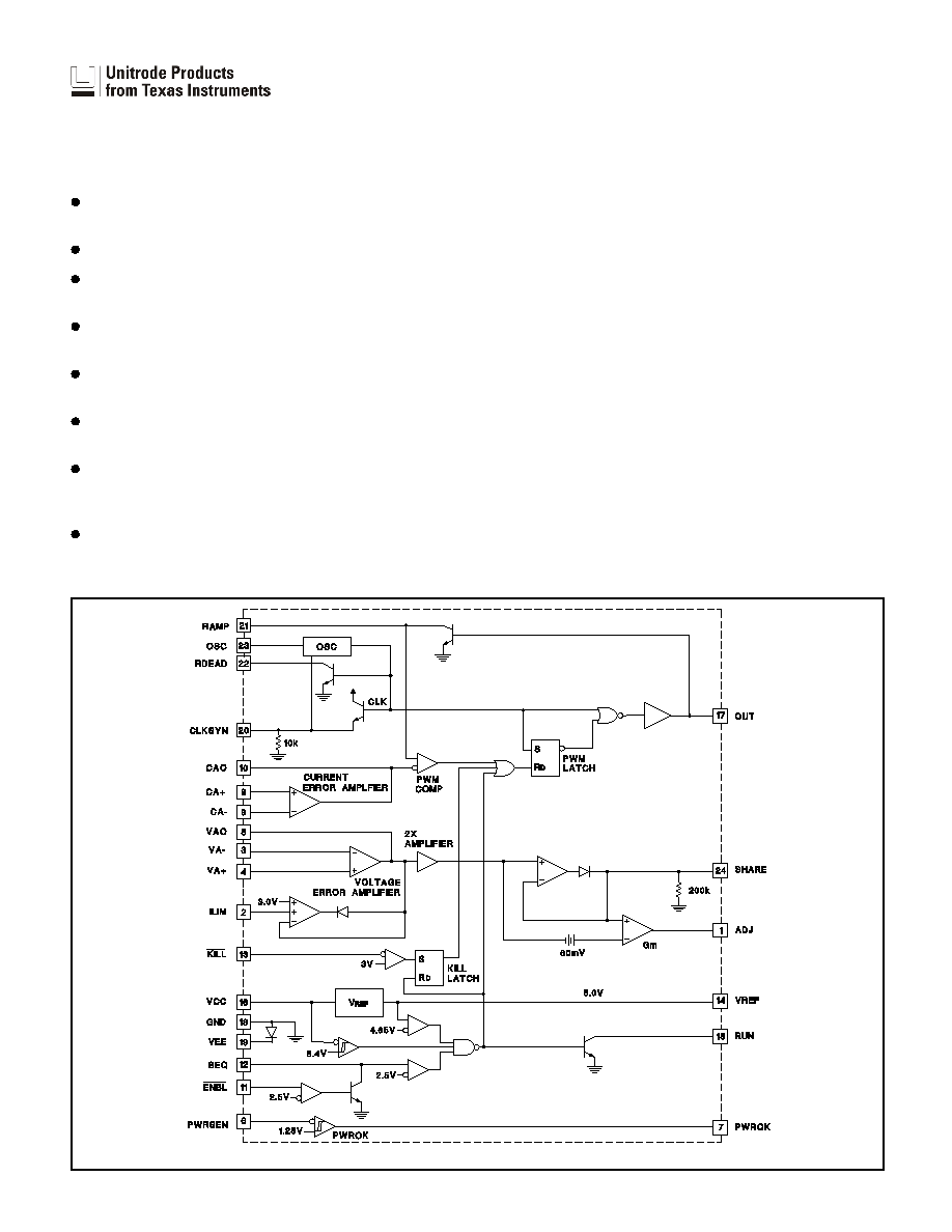
DESCRIPTION
The UC1826 family of average current mode controllers accurately accom-
plishes secondary side average current mode control. The secondary side
output voltage is regulated by sensing the output voltage and differentially
sensing the AC switching current. The sensed output voltage drives a volt-
age error amplifier. The AC switching current, monitored by a current sense
resistor, drives a high bandwidth, low offset current error amplifier. The out-
put of the voltage error amplifier can be used to drive the current amplifier
which filters the measured inductor current. Fast transient response is ac-
complished by utilizing voltage feedforward in generating the PWM ramp.
The UC1826 features load share, oscillator synchronization, undervoltage
lockout, and programmable output control. Multiple chip operation can be
achieved by connecting up to ten UC1826 chips in parallel. The SHARE
bus and CLKSYN bus provide load sharing and synchronization to the fast-
est oscillator respectively. With its tailored bandwidth, the UC1826 provides
excellent noise immunity and is an ideal controller to achieve high power,
secondary side average current mode control.
Secondary Side Average Current Mode Controller
FEATURES
Practical Secondary Side Control of
Isolated Power Supplies
1MHz Operation
Tailored Loop Bandwidth Provides
Excellent Noise Immunity
Voltage Feedforward Provides
Superior Transient Response
Accurate Programmable Maximum
Duty Cycle
Multiple Chips Can be Synchronized
to Fastest Oscillator
Wide Gain Bandwidth Product
(70MHz, Acl>10) Current Error
Amplifier
Up to Ten Devices Can Easily Share
a Common Load
SLUS331 - JULY 1995
BLOCK DIAGRAM
UDG-95013
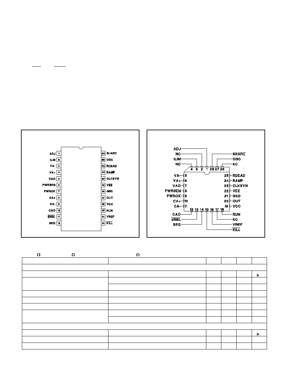
Pin Numbers refer to 24-pin packages.
2
UC1826
UC2826
UC3826
PLCC-28 (Top View)
Q Packages
ABSOLUTE MAXIMUM RATINGS
Supply Voltage (VCC) . . . . . . . . . . . . . . . . . . . . . . . . . . . . . 20V
Output Current Source or Sink . . . . . . . . . . . . . . . . . . . . . . 0.3A
Analog Input Voltages . . . . . . . . . . . . . . . . . . . . . . . ≠0.3V to 7V
ILIM, KILL, SEQ, ENBL, RUN, PWRSEN, PWROK ≠0.3V to 7V
CLKSYN Current Source . . . . . . . . . . . . . . . . . . . . . . . . . 20mA
RUN Current Sink . . . . . . . . . . . . . . . . . . . . . . . . . . . . . . . 20mA
SEQ Current Sink . . . . . . . . . . . . . . . . . . . . . . . . . . . . . . . 20mA
RDEAD Current Sink . . . . . . . . . . . . . . . . . . . . . . . . . . . . 20mA
RAMP Current Sink . . . . . . . . . . . . . . . . . . . . . . . . . . . . . 20mA
Share Bus Voltage (voltage with respect to GND) . . 0V to 6.2V
ADJ Voltage (voltage with respect to GND) . . . . . . 0.9V to 6.3V
VEE (voltage with respect to GND) . . . . . . . . . . . . . . . . . ≠1.5V
CONNECTION DIAGRAMS
ELECTRICAL CHARACTERISTICS:
Unless otherwise stated these specifications apply for T
A
= ≠55∞C to +125∞C for
UC1826; ≠40∞C to +85∞C for UC2826; and 0∞C to +70∞C for UC3826; VCC = 12V, VEE = GND, Output no load, C
T
= 345pF,
R
T
= 4k , RDEAD = 1000 , C
RAMP
= 345pF, R
RAMP
= 35.2k , R
CLKSYN
= 1k, T
A
= T
J
.
PARAMETER
TEST CONDITIONS
MIN
TYP
MAX
UNITS
Current Error Amplifier
Ib
0.5
3
A
Vio
T
A
= +25∞C
0.75
3
mV
Over Temperature
5
mV
Avo
60
90
dB
GBW (Note 2)
Acl = 10, R
IN
= 1k, CC = 15pF, f = 200kHz (Note 1)
45
70
MHz
Vol
I
O
= 1mA, Voltage above VEE
0.5
V
Voh
I
O
= 0mA
3.8
V
I
O
= ≠1mA
3.5
V
Voltage Error Amplifier
Ib
0.5
3
A
Vio
5
mV
Avo
60
90
dB
Storage Temperature . . . . . . . . . . . . . . . . . . . ≠65∞C to +150∞C
Junction Temperature . . . . . . . . . . . . . . . . . . . ≠65∞C to +150∞C
Lead Temperature (Soldering, 10 sec.) . . . . . . . . . . . . . +300∞C
All voltages with respect to VEE except where noted; all cur-
rents are positive into, negative out of the specified terminal.
Consult Packaging Section of Databook for thermal limitations
and considerations of packages.
RECOMMENDED OPERATING CONDITIONS
Input Voltage . . . . . . . . . . . . . . . . . . . . . . . . . . . . . . . 8V to 20V
Sink/Source Output Current . . . . . . . . . . . . . . . . . . . . . . 250mA
Timing Resistor R
T
. . . . . . . . . . . . . . . . . . . . . . . . . . 1k to 200k
Timing Capacitor C
T
. . . . . . . . . . . . . . . . . . . . . . . . 75pF to 2nF
DIL-24, SOIC-24 (Top View)
J or N, DW Packages

3
UC1826
UC2826
UC3826
ELECTRICAL CHARACTERISTICS:
Unless otherwise stated these specifications apply for T
A
= ≠55∞C to +125∞C for
UC1826; ≠40∞C to +85∞C for UC2826; and 0∞C to +70∞C for UC3826; VCC = 12V, VEE = GND, Output no load, C
T
= 345pF,
R
T
= 4k , RDEAD = 1000 , C
RAMP
= 345pF, R
RAMP
= 35.2k , R
CLKSYN
= 1k, T
A
= T
J
.
PARAMETER
TEST CONDITIONS
MIN
TYP
MAX
UNITS
Voltage Error Amplifier (cont.)
GBW (Note 2)
f = 200kHz
7
MHz
Vol
I
O
= 175mA, Volts above VEE
0.6
V
Voh
ILIM = 3V
2.85
3
3.15
V
Voh-ILIM
Tested ILIM = 0.5V, 1.0V, 2.0V
≠100
100
mV
2X Amplifier and Share Amplifier
V offset (b; y = mx + b)
20
mV
GAIN (m; y = mx + b)
Slope with AV
OUT
= 1V and 2V
1.98
2.02
V
GBW (Note 2)
100
kHZ
R
SHARE
VCC = 0, V
SHARE/ISHARE
200
k
Total Offset
Negative supply is VEE, GND Open,VAO = GND
≠75
0
75
mV
Vol
VAO = Voltage Amp Vol, Volts above VEE
0.2
0.45
0.6
V
Voh
I
O
= 0mA, ILIM = 3V, VAO = Voltage Amp Voh
5.7
6
6.3
V
I
O
= ≠1mA, ILIM = 3V, VAO = Voltage Amp Voh
5.7
6
6.3
V
Adjust Amplifier
Vio
40
60
80
mV
gm
I
O
= ≠2 A to 2 A, C
ADJ
= 0.1 F
≠0.1
≠0.3
mS
Vol
I
OUT
= 0
0.9
1
1.1
v
I
OUT
= 2 A
0.85
1
1.15
V
Voh
I
OUT
= 0, V
SHARE
= 6.5V
5.7
6
6.3
V
I
OUT
= ≠2 A, V
SHARE
= 6.5V
5.7
6
6.3
V
Oscillator
Frequency
450
500
550
kHz
Max Duty Cycle
72
76
80
%
OSC Ramp Amplitude
2
2.2
2.4
V
Ramp Saturation
I
O
= 10mA, OSC = 0V
0.44
0.8
V
Clock Driver/SYNC (CLKSYN)
Vol
0.02
0.2
V
Voh
3.6
V
R
CLKSYN
= 200
3.5
V
I
SOURCE
25
mA
R
CLKSYN
VCC = 0, V
CLKSYN/
I
CLKSYN
10
k
V
TH
1.5
V
VREF Comparator
Turn-on Threshold
4.65
V
Hysteresis
0.4
V
VCC Comparator
Turn-on Threshold
7.9
8.4
8.9
V
Hysteresis
0.4
V
PWR Sense Comparator
Voltage Threshold
1.25
V
Vol
I
O
= 1mA
0.3
0.4
V
Voh
I
O
= ≠100 A
4
V
KILL Comparator
Voltage Threshold
3
V

4
UC1826
UC2826
UC3826
ELECTRICAL CHARACTERISTICS:
Unless otherwise stated these specifications apply for T
A
= ≠55∞C to +125∞C for
UC1826; ≠40∞C to +85∞C for UC2826; and 0∞C to +70∞C for UC3826; VCC = 12V, VEE = GND, Output no load, C
T
= 345pF,
R
T
= 4k , RDEAD = 1000 , C
RAMP
= 345pF, R
RAMP
= 35.2k , R
CLKSYN
= 1k, T
A
= T
J
.
PARAMETER
TEST CONDITIONS
MIN
TYP
MAX
UNITS
Sequence Comparator
Voltage Threshold
2.5
V
SEQ SAT
I
O
= 10mA
0.25
V
Enable Comparator
Voltage Threshold
2.5
V
RUN SAT
I
O
= 10mA
0.2
V
Reference
VREF
T
A
= 25∞C
4.95
5
5.05
V
VCC = 15V
4.9
5.1
V
Line Regulation
10 < VCC < 20
3
15
mV
Load Regulation
0 < I
O
< 10mA
3
15
mV
Short Circuit I
VREF = 0V
30
60
90
mA
Output Stage
Rise Time
C
L
= 100pF
10
20
ns
Fall Time
C
L
= 100pF
10
20
ns
Voh
VCC > 11V, I
O
=≠10mA
8.0
8.
8.8
V
I
O
= ≠200mA
7.8
V
Vol
I
O
= 200mA
3.0
V
I
O
= 10mA
0.5
V
Virtual Ground
V
GND
-VEE
VEE is externally supplied, GND is floating
and used as Signal GND.
0.2
0.75
V
Icc
Icc (run)
21
30
mA
Note 1: Ensured by design. not 100% tested in production.
Note 2: Unless otherwise specified all voltages are with respect to GND. Currents are positive into, negative out of the
specified terminal.
ADJ: The output of the transconductance (gm = ≠0.1mS)
amplifier adjusts the control voltage to maintain equal
current sharing. The chip sensing the highest output cur-
rent will have its output clamped to 1V. A resistor divider
between VREF and ADJ drives the control voltage (VA+)
for the voltage amplifier. Each slave unit's ADJ voltage in-
creases (to a maximum of 6V) its control voltage (VA+)
until its load current is equal to the master. The 60mV in-
put offset on the gm amplifier ensures that the unit sens-
ing the highest load current is chosen as the master. The
60mV offset is ensured by design to be greater than the
inherent offset of the gm amplifier and the buffer ampli-
fier. While the 60mV offset represents an error in current
sharing, the gain of the current and 2X amplifiers re-
duces it to only 30mV. The total current sense gain is the
current amplifier gain. This pin needs a 0.1 F capacitor
to compensate the amplifier.
CA≠, CA+: The inverting and non-inverting inputs to the
current error amplifier. This amplifier needs a capacitor
between CA≠ and CAO to set its dominant pole.
CAO: The output of the current error amplifier which is
internally clamped to 4V. It is internally connected to the
inverting input of the PWM comparator.
CLKSYN: The clock and synchronization pin for the os-
cillator. This is a bidirectional pin that can be used to syn-
chronize several chips to the fastest oscillator. Its input
synchronization threshold is 1.4V. The CLKSYN voltage
is 3.6V when the oscillator capacitor C
T
is being dis-
charged, otherwise it is 0V.
PIN DESCRIPTIONS

5
UC1826
UC2826
UC3826
ENBL: The active low input with a 2.5V threshold en-
ables the output to switch. SEQ and RUN are driven low
when ENBL is above its 2.5V threshold.
GND: The signal ground used for the voltage sense am-
plifier, current error amplifier, current error amplifier, volt-
age reference, 2X amplifier, and share amplifier. The
output sink transistor is wired directly to this pin.
KILL: The active low input with a 3.0V threshold stops
the output from switching. Once this function is activated
RUN must be cycled low by driving KILL above 3.0V and
either resetting the power to the chip (VCC) or resetting
the ENBL signal.
ILIM: A voltage on this pin programs the voltage error
amplifier's Voh clamp. The voltage error amplifier output
represents the average output current. The Voh clamp
consequently limits the output current. If ILIM is tied to
VREF, it defaults to 3.0V. A voltage less than 3.0V con-
nected to ILIM clamps the voltage error amplifier at this
voltage and consequently limits the maximum output cur-
rent.
OSC:The oscillator ramp (not to be confused with PWM
ramp) pin has a capacitor C
T
to ground and two resistors
in series R
T
and R
DEAD
to VREF. The total resistance of
R
T
and R
DEAD
divided by VREF ≠ V
OSC
sets exponential
charge current. The oscillator charges from 1.2V to 3.4V
until the output transitions low. At this time an open col-
lector transistor is turned on and discharges the C
T
ca-
pacitor through RDEAD.
The charge time is approximately T
CHARGE
= 2(R
T
+
R
DEAD
)
∑C
T
when the R
DEAD
resistor is used.
The dead time is approximately T
DISCHARGE
= 2
∑ R
DEAD
∑ C
T
.
( )
1
1
Frequency
T
T
CHARGE
DISCHARGE
+
( )
2
Maximum Duty Cycle
T
T
T
CHARGE
CHARGE
DISCHARGE
+
The C
T
capacitance should be increased by approxi-
mately 40pF to account for parasitic capacitance.
OUT: The output of the PWM driver. It has an upper
clamp of 8.5V. The peak current sink and source are
250mA. All UVLO, SEQ, ENBL, and KILL logic either en-
able or disable the output driver.
PWRSEN: This pin is the input to the PWROK compara-
tor.
PWROK: The output pin from the PWROK comparator. It
has a 300 A current source output when driven high.
RAMP: An open collector that can sink 20mA to dis-
charge the oscillator capacitor. An RC is tied between
VCC and GND to accomplish feedforward. The PWM
output drives this pin. When the output is high, the tran-
sistor is off enabling the charging of the RAMP capacitor.
When the output transitions low, the transistor is turned
on discharging the RAMP capacitor. The voltage at
RAMP rises from 0.2V to near 4V at maximum duty cy-
cle. Although this is an exponential ramp at high VCC
voltage the ramp appears linear.
RDEAD: The pin that programs the maximum duty cycle
by connecting a resistor between it and OSC. The maxi-
mum duty cycle is decreased by increasing this resistor
value which increases the discharge time. The dead time,
the time when the output is low, is 2
∑ R
DEAD
∑
C
T.
The C
T
capacitance should be increased by approximately 40pF
to account for parasitic capacitance.
RUN: This is an open collector logic output that signifies
when the chip is operational. RUN is pulled high to VREF
through an external resistor when VCC is greater than
8.4V, VREF is greater than 4.65V, SEQ is greater than
2.5V, and KILL lower than 3.0V. RUN connected to the
VA+ pin and to a capacitor to ground adds an RC rise
time on the VA+ pin initiating a soft start.
SEQ: The sequence pin allows the sequencing of startup
for multiple units. A resistor between VREF and SEQ and
a capacitor between SEQ and GND create a unique RC
rise time for each unit which sequences the output
startup.
SHARE:The nearly DC voltage representing the average
output current. This pin is wired directly to all SHARE
pins and is the load share bus.
VA≠, VA+: The inverting and non-inverting inputs to the
voltage error amplifier.
VAO: The output of the voltage error amplifier. Its Voh is
clamped with the ILIM pin.
VCC: The input voltage to the chip. The chip is opera-
tional between 8.4V and 20V.
VEE: The negative supply voltage to the chip which pow-
ers the lower voltage rail for all amplifiers. The chip is op-
erational if VEE is connected to GND or if GND is
floating. When voltage is applied externally to VEE, GND
becomes a virtual ground because of an internal diode
between VEE and GND. The GND current flows through
the forward biased diode and out VEE. GND is always
the signal ground from which the voltage reference and
all amplifier inputs are referenced.
VREF: The reference voltage equal to 5.0V.
PIN DESCRIPTIONS (cont.)

6
UC1826
UC2826
UC3826
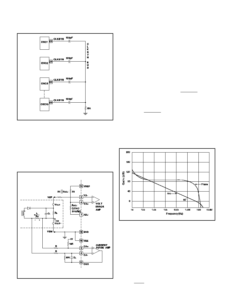
Figure 1. Oscillator Block with External Connections
PWM Oscillator: The chip has two pins that set RC time
constants. The resistor and capacitor tied to RAMP cre-
ate the ramp used as the input to the PWM comparator.
When the output pin OUT is high, RAMP charges until it
passes the PWM comparator threshold. The output is
then driven low and RAMP is discharged. The resistors
and capacitor on the OSC pin are used to set the PWM
operating frequency and its maximum duty cycle.
The oscillator block diagram with external wiring is shown
in Figure 1. OSC has a capacitor (C
T
) to ground and two
resistors in series (R
T
and R
DEAD
) to VREF. The total re-
sistance of R
T
and R
DEAD
divided by VREF - V
OSC
sets
the exponential charge current. The oscillator charges
from 1.2V to a 3.4V threshold with an RC time delay of 2
∑ C
T
∑ (R
DEAD
+ R
T
). After exceeding this threshold, the
RS flip-flop is set driving CLKSYN high and RDEAD low
which discharges C
T
. At this time an open collector tran-
sistor is turned on and discharges C
T
capacitor through
RDEAD with a RC time delay of 2
∑ C
T
∑ R
DEAD
. The os-
cillator and ramp waveforms are shown in Figure 2.
Equations to attain frequency and maximum duty cycle
are listed under the OSC pin description.
As shown in Figure 3, several oscillators are synchro-
nized to the highest free running frequency by connect-
ing 100pF capacitors in series with each CLKSYN pin
and connecting the other side of the capacitors together
forming the CLKSYN bus. The CLKSYN bus is then
pulled down to ground with a resistance of approximately
10k. Referring to Figure 1, the synchronization threshold
is 1.4V. The oscillator blanks any synchronization pulse
that occurs when OSC is below 2.5V. This allows units,
once they discharge below 2.5V, to continue through the
current
discharge
and
subsequent
charge
cycles
whether or not other units on the CLKSYN bus are still
synchronizing. This requires the frequency of all free run-
ning oscillators to be within 40% of each other to guaran-
tee synchronization.
Grounds, Voltage Sensing and Current Sensing: The
voltage is sensed directly at the load. Proper load sharing
requires the same sensed voltage for each power supply
connected
in
parallel. Referring
to
Figure
4,
the
CIRCUIT DESCRIPTION:
OSC
OUT
CLKSYN
RAMP
CAO
3.0-
1.0
Figure 2. Oscillator and PWM Output Waveform
UDG-95014-1
7
UC1826
UC2826
UC3826
positive sense voltage (VSP) connects to the voltage er-
ror amplifier inverting terminal (VA≠), the return lead for
the on-chip reference is used as the negative sense
(VSM). The current is sensed across the shunt resistor,
R
S
. The voltage across the shunt resistor is level shifted
up so that the maximum voltage across R
S
corresponds
to the voltage error amplifier Voh.
Figure 4 shows one recommended voltage and current
sensing scheme when VEE is connected to GND. The
signal ground is the negative sense point for the output
voltage and the positive sense point for the output cur-
rent. VEE is the negative supply for the current sense
amplifier. When it is separated from GND, it extends the
current sense amplifier's common mode input voltage
range to include VEE which is approximately ≠0.7V be-
low ground. The resistor R
ADJ
is used for load sharing.
The unit which is the master will force V
ADJ
to 1.0V.
Therefore, the regulated voltage being sensed is actually
VSP
VSM
VREF
V
R
R
R
V
ADJ
ADJ
ADJ
ADJ
≠
(
≠
)
=
∑
+
+
1
(
)
VSM
V V
V master VREF
V
ADJ
=
=
=
0
1
5
,
,
VSP
R
R
R
V
ADJ
ADJ
= ∑
+
+
4
1
1
The voltage at ADJ on the slave chips will increase forc-
ing their load currents to increase to match the master.
The AC frequency response of the voltage error amplifier
is shown in Figure 5.
Startup and Shutdown: Isolated power up can be ac-
complished using the UCC1889. Application Note U-149
is available for additional information.
The UC1826 offers several features that enhance startup
and shutdown. Soft start is accomplished by connecting
RUN to VA+ and a capacitor to ground. The resulting RC
rise time on the VA+ pin initiates a soft start. It can also
be accomplished by connecting RUN to ILIM. When RUN
is low it will command zero load current, guaranteeing a
soft start. The undervoltage lockout (UVLO) is a logical
AND of ENBL < 2.5V, SEQ > 2.5V, VCC > 8.4V and
CIRCUIT BLOCK DESCRIPTION (cont.)
Figure 3. Oscillator Synchronization Connection
Diagram
Figure 4. Voltage and Current Sense VEE Tied to
GND
m
Figure 5. AC Frequency Response of the Voltage
Error Amplifier
UDG-95016
UDG-95015
8
UC1826
UC2826
UC3826
VREF > 4.65V. The block diagram shows that the thresh-
olds are set by comparators. By placing an RC divider on
the SEQ pin, the enabling of multiple chips can be se-
quenced with different RC time constants. Similarly, dif-
ferent RC time constants on the ENBL pins can
sequence shutdown. The UVLO keeps the output from
switching; however the internal reference starts up with
VCC less than 8.4V. The KILL input shuts down the
switching of the chip. This can be used in conjunction
with an overvoltage comparator for overvoltage protec-
tion. In order to restart the chip after KILL has been initi-
ated, the chip must be powered down and then back up.
A pulse on the ENBL pin also accomplishes this without
actually removing voltage to the VCC pin.
Load Sharing: Load sharing is accomplished similarly to
the UC1907 except it has the added constraint of using
the sensed current for average current mode control. The
sensed current for the UC1826 has an AC component
that is amplified and then averaged. The voltage error
amplifier represents this average current. The voltage er-
ror amplifier output is the current command signal and its
voltage represents the average output load current. The
ILIM pin programs the upper clamp voltage of this ampli-
fier and consequently the maximum load current. A gain
of 2 amplifier connected between the voltage error ampli-
fier output and the share amplifier input increases the
current share resolution and noise margin. The average
current is used as an input to a source only load share
buffer amplifier. The output of this amplifier is the current
share bus. The IC with the highest sensed current will
have the highest voltage on the current share bus and
consequently act as the master. The 60mV input offset
guarantees that the unit sensing the highest load current
is chosen as the master.
The adjust amplifier is used by the remaining (slave) ICs
to adjust their respective references high in order to bal-
ance each IC's load current. The master's ADJ pin will be
at
its
1.0V
clamp
and
connected
back
to
the
non-inverting voltage error amplifier input through a high
value resistor. This requires the user to initially calculate
the control voltage with the ADJ pin at 1.0V.
VREF can be adjusted 150mV to 300mV which compen-
sates for 5% unit to unit reference mismatch and external
resistor mismatch. R
ADJ
will typically be 10 to 30 times
larger than R1. This also attenuates the overall variation
of the ADJ clamp of 1V ±100mV by a factor of 10 to 30,
contributing only a 3mV to 10mV additional delta to
VREF. Refer to the UC3907 Application Note U-130 for
further information on parallel power supply load sharing.
Current Control Loop: The current error amplifier (CEA)
needs its loop compensated externally. The zero crossing
can be calculated with Equation 3.
( )
(
)
3
0
1
2
Frequency dB
R
C
INV
COMP
=
∑
R
INV
is the input resistance at the inverting terminal CA≠
C
COMP
is the capacitance between C
A
≠ and CAO.
Although it is only unity gain stable for a BW of 7MHz,
the amplifier is typically configured with a differential gain
of at least 10, allowing the amplifier to operate with suffi-
cient phase margin at a GBW of 70MHz. A closed loop
gain of 10 attenuates the output by 20.8dB
20 8
20
1
11
.
log
=
∑
to the inverting terminal assuring stability. The amplifier's
gain fed back into the inverting terminal is less than unity
at 7MHz, where the phase margin begins to roll off. See
Figure 6 for a typical Bode plot.
The current error amplifier bandwidth is rolled off and
controlled by the voltage error amplifier output. The maxi-
mum load current is limited to approximately the maxi-
mum voltage across the shunt resistor (maximum of
200mV) divided by R
S
:
(
)
( )
( )
4
I
V
R
MAX LOAD
R S
S
=
ILIM sets the maximum current limit by setting the Voh
clamp on the voltage error amplifier. If ILIM is not set to
limit the Voh to be equal to the maximum voltage across
R
S
, VAO must be attenuated to match the maximum volt-
age V
RS
across the shunt resistor. By attenuating the
CIRCUIT BLOCK DESCRIPTION (cont.)
m
-
Figure 6. Current Error Amplifier Bode Plot
9
UC1826
UC2826
UC3826
maximum voltage at VAO to be equal to V
RS
, the current
control loop keeps the load from exceeding its current
limit. If the ILIM pin is connected to VREF, the Voh is set
at 3.0V. The maximum current limit clamp can be re-
duced by reducing the voltage on ILIM to less than 3.0V
as described in the ILIM pin description.
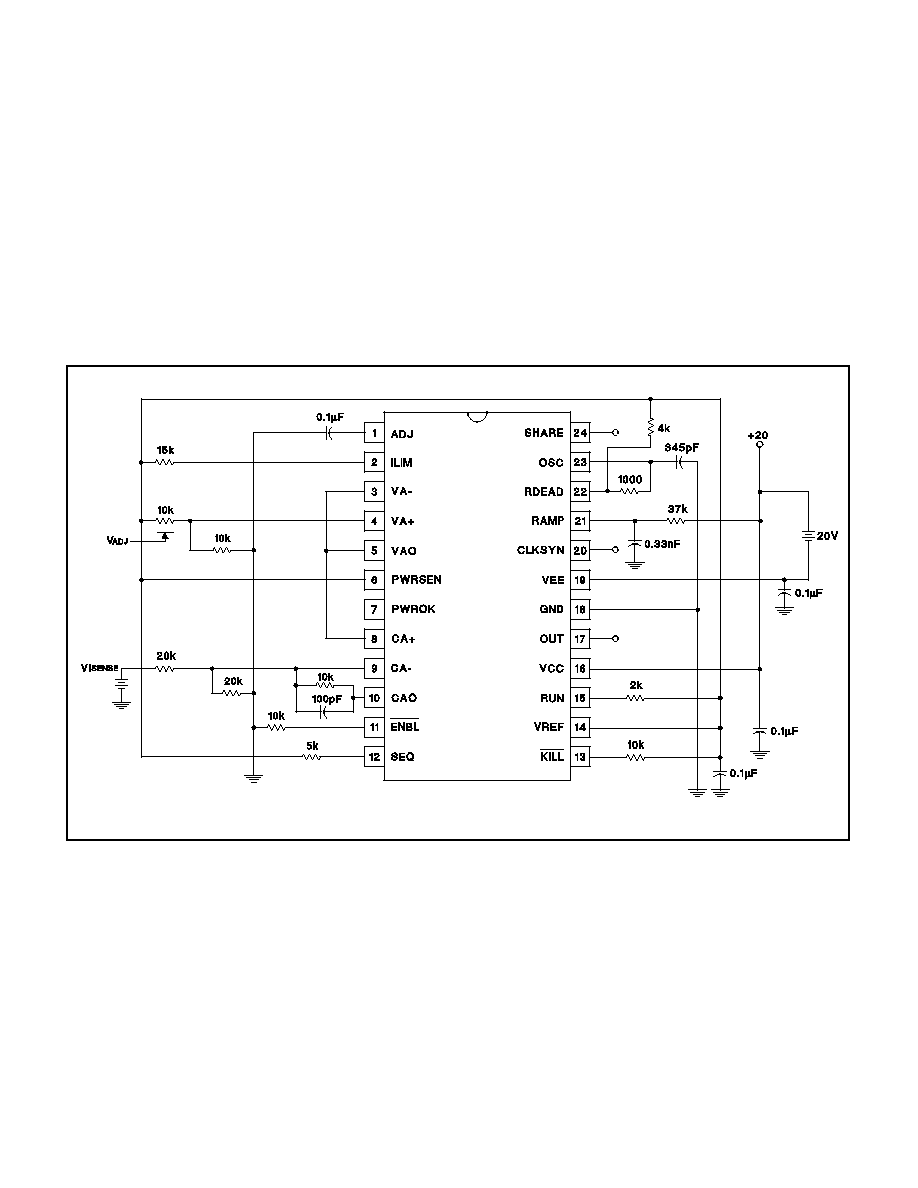
Design Example: Figure 7 is an open loop test that lets
the user test the circuit blocks discussed without having
to build an entire control loop. The pulse width can be
varied by either the V
ADJ
or the VI
SENSE
inputs. Figure 8
shows an isolated power supply using the UC1826 sec-
ondary side average current mode controller.
CIRCUIT BLOCK DESCRIPTION (cont.)
Figure 7. Open Loop Circuit
UDG-95017-1
10
UC1826
UC2826
UC3826
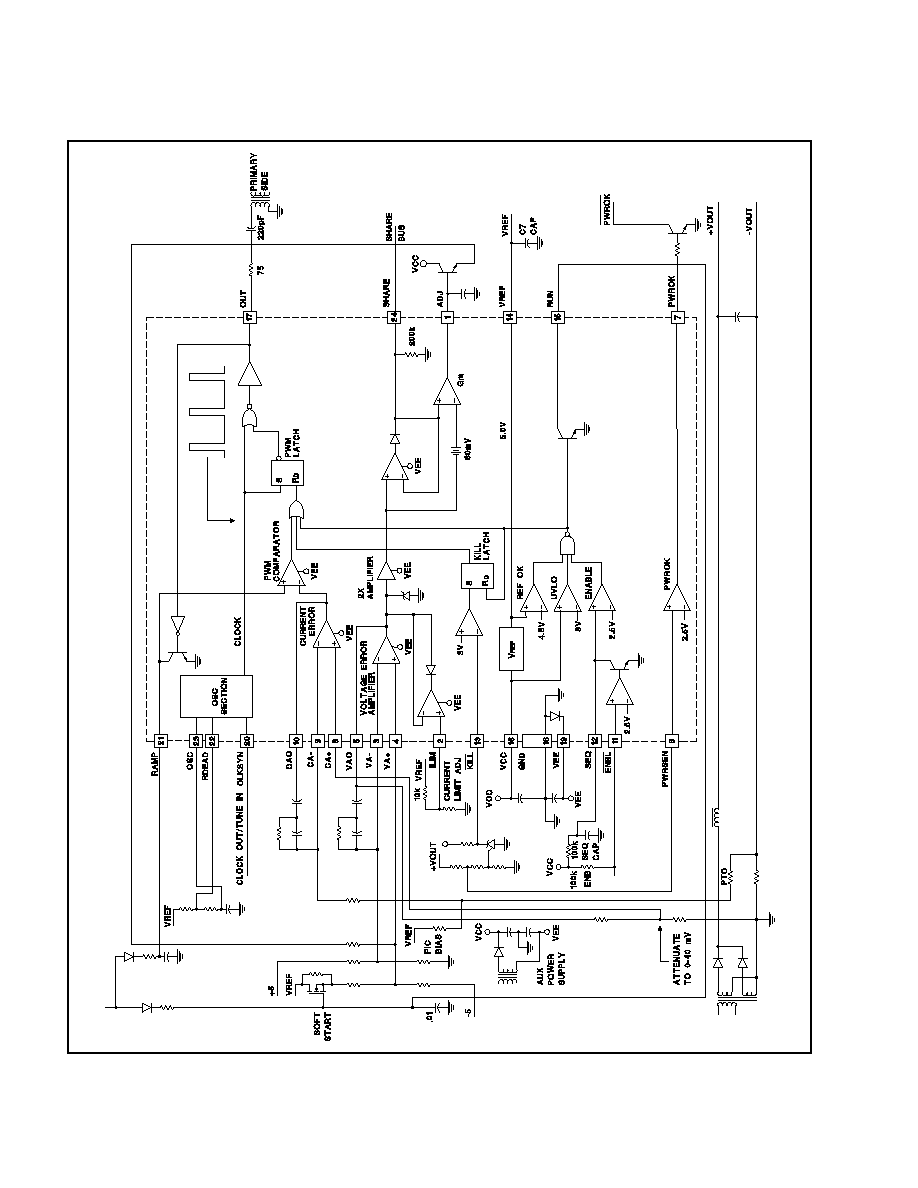
Figure 8. UC1826 Application Diagram

IMPORTANT NOTICE
Texas Instruments Incorporated and its subsidiaries (TI) reserve the right to make corrections, modifications,
enhancements, improvements, and other changes to its products and services at any time and to discontinue
any product or service without notice. Customers should obtain the latest relevant information before placing
orders and should verify that such information is current and complete. All products are sold subject to TI's terms
and conditions of sale supplied at the time of order acknowledgment.
TI warrants performance of its hardware products to the specifications applicable at the time of sale in
accordance with TI's standard warranty. Testing and other quality control techniques are used to the extent TI
deems necessary to support this warranty. Except where mandated by government requirements, testing of all
parameters of each product is not necessarily performed.
TI assumes no liability for applications assistance or customer product design. Customers are responsible for
their products and applications using TI components. To minimize the risks associated with customer products
and applications, customers should provide adequate design and operating safeguards.
TI does not warrant or represent that any license, either express or implied, is granted under any TI patent right,
copyright, mask work right, or other TI intellectual property right relating to any combination, machine, or process
in which TI products or services are used. Information published by TI regarding third≠party products or services
does not constitute a license from TI to use such products or services or a warranty or endorsement thereof.
Use of such information may require a license from a third party under the patents or other intellectual property
of the third party, or a license from TI under the patents or other intellectual property of TI.
Reproduction of information in TI data books or data sheets is permissible only if reproduction is without
alteration and is accompanied by all associated warranties, conditions, limitations, and notices. Reproduction
of this information with alteration is an unfair and deceptive business practice. TI is not responsible or liable for
such altered documentation.
Resale of TI products or services with statements different from or beyond the parameters stated by TI for that
product or service voids all express and any implied warranties for the associated TI product or service and
is an unfair and deceptive business practice. TI is not responsible or liable for any such statements.
Mailing Address:
Texas Instruments
Post Office Box 655303
Dallas, Texas 75265
Copyright
2002, Texas Instruments Incorporated