 | –≠–ª–µ–∫—Ç—Ä–æ–Ω–Ω—ã–π –∫–æ–º–ø–æ–Ω–µ–Ω—Ç: UC1834L | –°–∫–∞—á–∞—Ç—å:  PDF PDF  ZIP ZIP |
UC1834
UC2834
UC3834
High Efficiency Linear Regulator
FEATURES
∑
Minimum V
IN
- V
OUT
Less Than
0.5V At 5A Load With External
Pass Device
∑
Equally Usable For Either Positive
or Negative Regulator Design
∑
Adjustable Low Threshold Current
Sense Amplifier
∑
Under And Over-Voltage Fault Alert
With Programmable Delay
∑
Over-Voltage Fault Latch With
100mA Crowbar Drive Output
DESCRIPTION
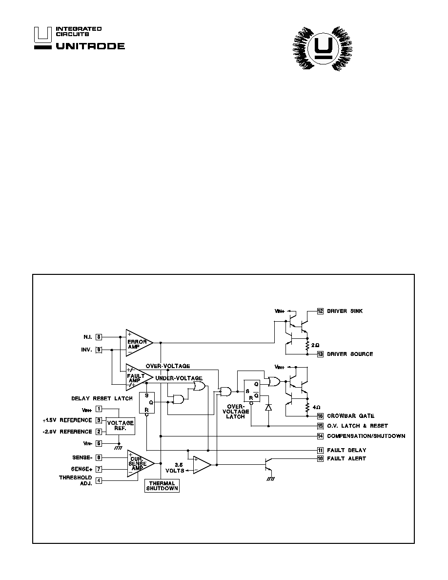
The UC1834 family of integrated circuits is optimized for the design of low
input-output differential linear regulators. A high gain amplifier and 200mA
sink or source drive outputs facilitate high output current designs which use
an external pass device. With both positive and negative precision refer-
ences, either polarity of regulator can be implemented. A current sense am-
plifier with a low, adjustable, threshold can be used to sense and limit
currents in either the positive or negative supply lines.
In addition, this series of parts has a fault monitoring circuit which senses
both under and over-voltage fault conditions. After a user defined delay for
transient rejection, this circuitry provides a fault alert output for either fault
condition. In the over-voltage case, a 100mA crowbar output is activated.
An over-voltage latch will maintain the crowbar output and can be used to
shutdown the driver outputs. System control to the device can be accom-
modated at a single input which will act as both a supply reset and remote
shutdown terminal. These die are protected against excessive power dissi-
pation by an internal thermal shutdown function.
BLOCK DIAGRAM
6/94

ABSOLUTE MAXIMUM RATINGS (Note 1)
Input Supply Voltage, V
IN
+ . . . . . . . . . . . . . . . . . . . . . . . . . 40V
Driver Current . . . . . . . . . . . . . . . . . . . . . . . . . . . . . . . . . 400mA
Driver Source to Sink Voltage . . . . . . . . . . . . . . . . . . . . . . . 40V
Crowbar Current . . . . . . . . . . . . . . . . . . . . . . . . . . . . . .
-
200mA
+1.5V Reference Output Current . . . . . . . . . . . . . . . . . .
-
10mA
Fault Alert Voltage . . . . . . . . . . . . . . . . . . . . . . . . . . . . . . . . 40V
Fault Alert Current . . . . . . . . . . . . . . . . . . . . . . . . . . . . . . 15mA
Error Amplifier Inputs . . . . . . . . . . . . . . . . . . . . . .
-
0.5V to 35V
Current Sense Inputs . . . . . . . . . . . . . . . . . . . . . .
-
0.5V to 40V
O.V. Latch Output Voltage . . . . . . . . . . . . . . . . . .
-
0.5V to 40V
O.V. Latch Output Current . . . . . . . . . . . . . . . . . . . . . . . . 15mA
Power Dissipation at T
A
= 25∞C . . . . . . . . . . . . . . . . . . 1000mW
Power Dissipation at T
C
= 25∞C. . . . . . . . . . . . . . . . . . 2000mW
Operating Junction Temperature . . . . . . . . . .
-
55∞C to +150∞C
Storage Temperature . . . . . . . . . . . . . . . . . . .
-
65∞C to +150∞C
Lead Temperature (soldering, 10 seconds). . . . . . . . . . . 300∞C
Note 1: Voltages are reference to V
IN
-
, Pin 5.
Currents are positive into, negative out of the specified
terminals.
Consult Packaging section of Databook for thermal
limitations and considerations of package.
UC1834
UC2834
UC3834
CONNECTION DIAGRAMS
DIL-16, SOIC-16 (TOP VIEW)
J or N Package, DW Package
PLCC-20, LCC-20 (TOP VIEW)
Q, L Packages
PACKAGE PIN FUNCTION
FUNCTION
PIN
N/C
1
V
IN
+
2
-
2.0V REF
3
+1.5V REF
4
Threshold Adjust
5
N/C
6
V
IN
-
7
Sense
-
8
Sense+
9
N.Inv. Input
10
N/C
11
Inv. Input
12
Fault Alert
13
Fault Delay
14
Driver Sink
15
N/C
16
Driver Source
17
Compensation/ Shutdown
18
O.V. Latch Output/Reset
19
Crowbar Gate
20
2
PARAMETER
TEST CONDITIONS
UC1834
UC2834
UC3834
UNITS
MIN
TYP
MAX
MIN
TYP
MAX
Turn-on Characteristics
Standby Supply Current
5.5
7
5.5
10
mA
+1.5 Volt Reference
Output Voltage
T
J
= 25∞C
1.485
1.5
1.515
1.47
1.5
1.53
V
T
J(MIN)
T
J
T
J(MAX)
1.47
1.53
1.455
1.545
Line Regulation
V
IN+
= 5 to 35V
1
10
1
15
mV
Load Regulation
I
OUT
= 0 to 2mA
1
10
1
15
mV
-2.0 Volt Reference (Note 2)
Output Voltage (Referenced
to V
IN
+
)
T
J
= 25∞C
-
2.04
-
2
-
1.96
-
2.06
-
2
-
1.94
V
T
J(MIN)
T
J
T
J(MAX)
-
2.06
-
1.94
-
2.08
-
1.92
Line Regulation
V
IN+
= 5 to 35V
1.5
15
1.5
20
mV
Output Impedance
2.3
2.3
k
Error Amplifier Section
Input Offset Voltage
V
CM
= 1.5V
1
6
1
10
mV
Input Bias Current
V
CM
= 1.5V
-
1
-
4
-
1
-
8
µ
A
Input Offset Current
V
CM
= 1.5V
0.1
1
0.1
2
µ
A
Small Signal Open Loop Gain Output @ Pin 14, Pin 12 = V
IN+
Pin 13, 20
to V
IN
-
50
65
50
65
dB
CMRR
V
CM
= 0.5 to 33V, V
IN+
= 35V
60
80
60
80
dB
PSRR
V
IN+
= 5 to 35V, V
CM
= 1.5V
70
100
70
100
dB
Driver Section
Maximum Output Current
200
350
200
350
mA
Saturation Voltage
I
OUT
= 100mA
0.5
1.2
0.5
1.5
V
Output Leakage Current
Pin 12 = 35V, Pin 13 = V
IN
-
, Pin 14 = V
IN
-
0.1
50
0.1
50
µ
A
Shutdown Input Voltage
at Pin 14
I
OUT
100
µ
A, Pin 13 = V
IN
-
, Pin 12 =
V
IN+
0.4
1
0.4
1
V
Shutdown Input Current
at Pin 14
Pin 14 = V
IN
-
, Pin 12 = V
IN+
I
OUT
100
µ
A, Pin 13 = V
IN
-
-
100
-
150
-
100
-
150
µ
A
Thermal Shutdown (Note 3)
165
165
∞C
Fault Amplifier Section
Under- and Over-Voltage
Fault Threshold
V
CM
= 1.5V, @ E/A Inputs
120
150
180
110
150
190
mV
Common Mode Sensitivity
V
IN+
= 35V, V
CM
= 1.5 to 33V
-
0.4
-
0.8
-
0.4
-
1.0
%/v
Supply Sensitivity
V
CM
= 1.5V, V
IN+
= 5 to 35V
-
0.5
-
1.0
-
0.5
-
1.2
%/V
Fault Delay
30
45
60
30
45
60
ms/
µ
F
Fault Alert Output Current
2
5
2
5
mA
Fault Alert Saturation Voltage I
OUT
= 1mA
0.2
0.5
0.2
0.5
V
O.V. Latch Output Current
2
4
2
4
mA
O.V. Latch Saturation Voltage I
OUT
= 1mA
1.0
1.3
1.0
1.3
V
O.V. Latch Output Reset
Voltage
0.3
0.4
0.6
0.3
0.4
0.6
V
Crowbar Gate Current
-
100
-
175
-
100
-
175
mA
Crowbar Gate Leakage
Current
V
IN+
= 35V, Pin 16 = V
IN
-
-
0.5
-
50
-
0.5
-
50
µ
A
Note 2: When using both the 1.5V and
-
2.0V references the current out of pin 3 should be balanced by an equivalent current into
Pin 2. The
-
2.0V output will change
-
2.3mV per
µ
A of imbalance.
Note 3: Thermal shutdown turns off the driver. If Pin 15 (O.V. Latch Output) is tied to Pin 14 (Compensation/Shutdown) the
O.V. Latch will be reset.
UC1834
UC2834
UC3834
ELECTRICAL CHARACTERISTICS:
Unless otherwise stated, these specifications apply for T
A
=
-
55∞C to +125∞C
for the UC1834,
-
40∞C to +85∞C for the UC2834, and 0∞C to +70∞C for the
UC3834. V
IN+
= 15V, V
IN
-
= 0V, T
A
= T
J.
3
PARAMETER
TEST CONDITIONS
UC1834
UC2834
UC3834
UNITS
MIN
TYP
MAX
MIN
TYP
MAX
Current Sense Amplifier Section
Threshold Voltage
Pin 4 Open, V
CM
= V
IN+
or V
IN
-
130
150
170
120
150
180
mV
Pin 4 = 0.5V, V
CM
= V
IN+
or V
IN
-
40
50
60
30
50
70
Threshold Supply Sensitivity
Pin 4 Open, V
CM
= V
IN
-
,
V
IN+
= 5 to 35V
-
0.1
-
0.3
-
0.1
-
0.5
%/V
Adj. Input Current
Pin 4 = 0.5V
-
2
-
10
-
2
-
10
µ
A
Sense Input Bias Current
V
CM
= V
IN+
100
200
100
200
µ
A
V
CM
= V
IN
-
-
100
-
200
-
100
-
200
UC1834
UC2834
UC3834
ELECTRICAL CHARACTERISTICS:
Unless otherwise stated, these specifications apply for T
A
=
-
55∞C to +125∞C
for the UC1834,
-
40∞C to +85∞C for the UC2834, and 0∞C to +70∞C for the
UC3834. V
IN+
= 15V, V
IN
-
= 0V. T
A
= T
J
Differential Voltage at Current Sense
Inputs - mV (reference to sense
-
input)
Current Sense Threshold Adjustment
Current Limiting Knee Characteristics
Error Amplifier Gain and Phase
Frequency Response
Current Sense Amplifier Gain and Phase
Frequency Response
4

UC1834
UC2834
UC3834
Both the current sense and error amplifiers on the UC1834
are transconductance type amplifiers. As a result, their volt-
age gain is a direct function of the load impedance at their
shared output pin, Pin 14. Their small signal voltage gain as
a function of load and frequency is nominally given by;
A
V E
/
A
=
Z
L
(
f
)
700
and A
V C. S.
/
A
=
Z
L
(
f
)
70
for: f
500kHz and |Z
L
(f)|
1 M
Where:
A
V
=Small Signal Voltage Gain to pin 14.
Z
L
(f) = Load Impedance at Pin 14.
The UC1834 fault delay circuitry prevents the fault outputs
from responding to transient fault conditions. The delay reset
latch insures that the full, user defined, delay passes before an
over-voltage fault response occurs. This prevents unnecessary
crowbar, or latched-off conditions, from occurring following
sharp under-voltage to over-voltage transients.
The crowbar output on the UC1834 is activated following a
sustained over-voltage condition. The crowbar output remains
high as long as the fault condition persists, or, as long as the
over-voltage latch is set. The latch is set with an over-voltage
fault if the voltage at Pin 15 is above the latch reset threshold,
typically 0.4V. When the latch is set, its Q
-
output will pull Pin
15 low through a series diode. As long as a nominal pull-up
load exists, the series diode prevents Q
-
from pulling Pin 15
below the reset threshold. However, Pin 15 is pulled low
enough to disable the driver outputs if Pins 15 and 14 are
tied together. With Pin 15 and 14 common, the regulator
will latch off in response to an over-voltage fault. If the
fault condition is cleared and Pins 14 and 15 are momen-
tarily pulled below the latch reset threshold, the driver out-
puts are re-enabled.
APPLICATION INFORMATION
Foldback Current Limiting
Setting the Threshold Adjust Voltage (V
ADJ
)
5