FEATURES
∑
Complete Control for a High Current,
Low Dropout, Linear Regulator
∑
Fixed 5V or Adjustable Output Voltage
∑
Accurate 2.5A Current Limiting with
Foldback
∑
Internal Current Sense Resistor
∑
Remote Sense for Improved Load
Regulation
∑
External Shutdown
∑
Under-Voltage Lockout and Reverse
Voltage Protection
∑
Thermal Shutdown Protection
∑
8 Pin Mini-Dip Package
(Surface Mount also Available)
DESCRIPTION
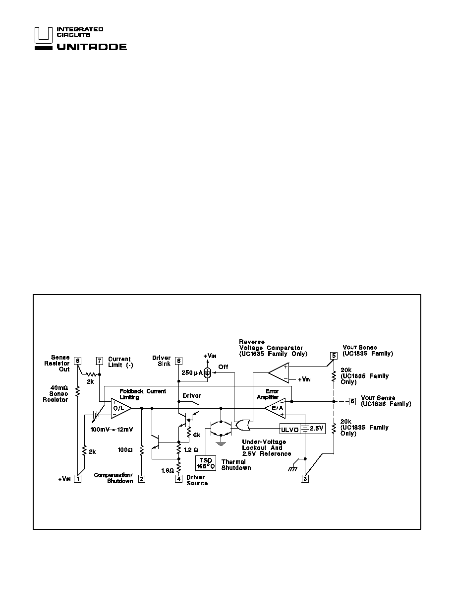
The UC1835/6 families of linear controllers are optimized for the de-
sign of low cost, low dropout, linear regulators. Using an external pass
element, dropout voltages of less than 0.5V are readily obtained.
These devices contain a high gain error amplifier, a 250mA output
driver, and a precision reference. In addition, current sense with fold-
back provides for a 2.5A peak output current dropping to less than
0.5A at short circuit.
These devices are available in fixed, 5V, (UC1835), or adjustable,
(UC1836), versions. In the fixed 5 volt version, the only external parts
required are an external pass element, an output capacitor, and a com-
pensation capacitor. On the adjustable version the output voltage can
be set anywhere from 2.5V to 35V with two external resistors.
Additional features of these devices include under-voltage lockout for
predictable start-up, thermal shutdown and short circuit current limiting
to protect the driver device. On the fixed voltage version, a reverse
voltage comparator minimizes reverse load current in the event of a
negative input to output differential.
High Efficiency Regulator Controller
BLOCK DIAGRAM
Note: Pin numbers refer to 8-Pin DIL Package
UC1835 UC1836
UC2835 UC2836
UC3835 UC3836
8/94
UC1835 UC1836
UC2835 UC2836
UC3835 UC3836
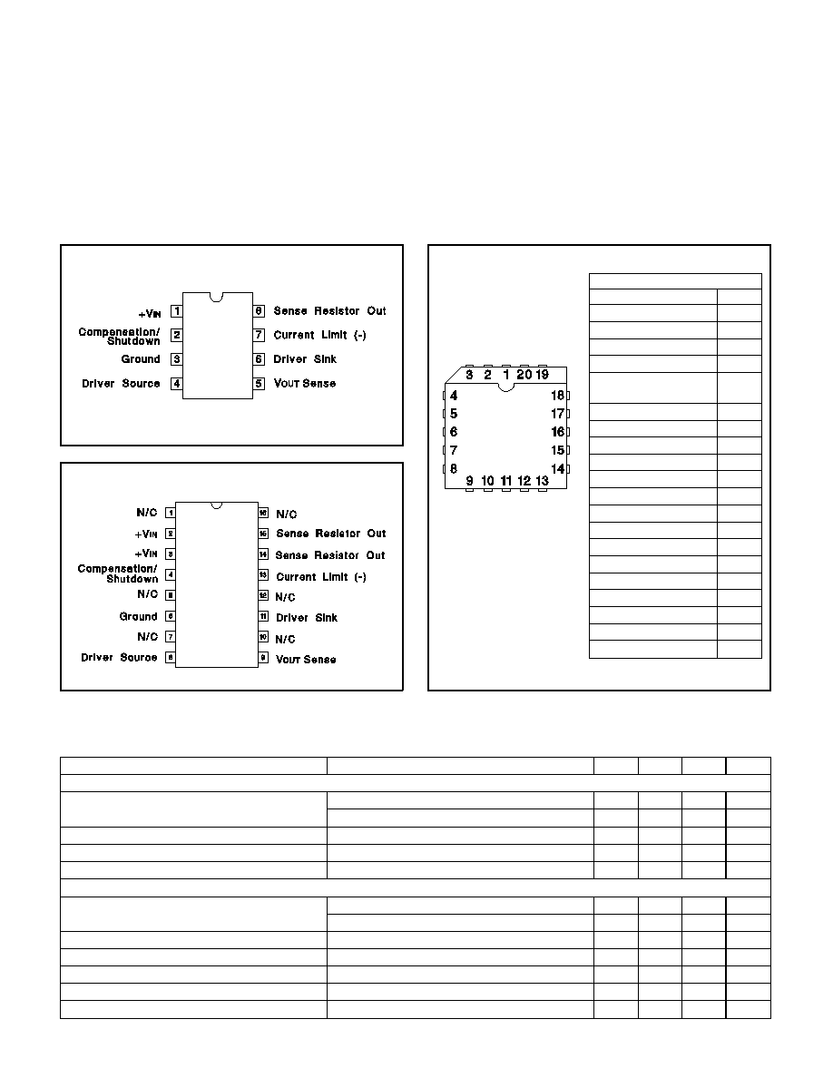
SOIC-16 (TOP VIEW)
DW Package
CONNECTION DIAGRAMS
PACKAGE PIN FUNCTION
FUNCTION
PIN
N/C
1
+V
IN
2
+V
IN
3
N/C
4
Compensation/
Shutdown
5
N/C
6
Ground
7
N/C
8
N/C
9
Driver Source
10
N/C
11
V
OUT
Sense
12
N/C
13
N/C
14
Driver Sink
15
N/C
16
Current Limit (-)
17
N/C
18
Sense Resistor Out
19
Sense Resistor Out
20
DIL-8, SOIC-8 (TOP VIEW)
N or J Package, D Package
PLCC-20, LCC-20
(TOP VIEW)
Q, L Packages
Input Supply Voltage (+V
IN
) . . . . . . . . . . . . . . . . ≠1.0V to + 40V
Driver Output Current (Sink or Source) . . . . . . . . . . . . . 600mA
Driver Source to Sink Voltage . . . . . . . . . . . . . . . . . . . . . + 40V
Maximum Current Through Sense Resistor. . . . . . . . . . . . . . 4A
V
OUT
Sense Input Voltage . . . . . . . . . . . . . . . . . . ≠.3V to + 40V
Power Dissipation at T
A
= 25∞C (Note 2) . . . . . . . . . . . 1000mW
Power Dissipation at T
C
= 25∞C (Note 2) . . . . . . . . . . . 2000mW
Operating Junction Temperature . . . . . . . . . . . -55∞C to +150∞C
Storage Temperature . . . . . . . . . . . . . . . . . . . . -65∞C to +150∞C
Lead Temperature (Soldering, 10 Seconds) . . . . . . . . . . 300∞C
Note 1: Voltages are referenced to ground, (Pin 3). Currents are
positive into, negative out of, the specified terminals.
Consult Packaging Section of Databook for thermal
considerations and limitations of packages.
ELECTRICAL CHARACTERISTICS:
Unless otherwise stated, specifications hold for T
A
= 0∞C to + 70∞C for the
UC3835/6, ≠25∞C to + 85∞C for the UC2835/6, and ≠55∞C to +125∞C for the
UC1835/6, +V
IN
= 6V, Driver Source= 0V, Driver Sink = 5V, T
A
= T
J
.
PARAMETER
TEST CONDITIONS
MIN.
TYP.
MAX. UNITS
Input Supply
Supply Current
+V
IN
= 6V
2.75
4.0
mA
+V
IN
= 40V
3.75
6.0
mA
UVLO Threshold
+V
IN
Low to High, V
OUT
Sense = 0V
3.9
4.4
4.9
V
Threshold Hysteresis
0.1
0.35
V
Reverse Current
+V
IN
= -1.0V, Driver Sink Open
6.0
20
mA
Regulating Voltage and Error Amplifier (UC1835 Family Only)
Regulating Level at V
OUT
Sense (V
REG
)
Driver Current = 10mA, T
J
= 25∞C
4.94
5.0
5.06
V
Over Temperature
4.9
5.1
V
Line Regulation
+V
IN
= 5.2V + 35V
15
40
mV
Load Regulation
Driver Current = 0 to 250mA
6.0
25
mV
Bias Current at V
OUT
Sense
V
OUT
Sense = 5.0V
75
125
210
µ
A
Error Amp Transconductance
±
100
µ
A at Compensation/Shutdown Pin
0.8
1.3
2.0
mS
Maximum Compensation Output Current
Sink or Source, Driver Source Open
90
200
260
µ
A
ABSOLUTE MAXIMUM RATINGS (Note 1)
2
UC1835 UC1836
UC2835 UC2836
UC3835 UC3836
PARAMETER
TEST CONDITIONS
MIN.
TYP.
MAX. UNITS
Regulating Voltage and Error Amplifier (UC1836 Family Only)
Regulating Level at V
OUT
Sense (V
REG
)
Driver Current = 10mA, T
J
= 25∞C
2.47
2.5
2.53
V
Over Temperature
2.45
2.55
V
Line Regulation
+V
IN
= 5.2V to 35V
6.0
20
mV
Load Regulation
Driver Current = 0 to 250mA
3.0
15
mV
Bias Current at V
OUT
Sense
V
OUT
Sense =2.5V
-1.0
-0.2
µ
A
Error Amp Transconductance
±
100
µ
A at Compensation/Shutdown Pin
0.8
1.3
2.0
mS
Maximum Compensation Output Current
Sink or Source, Driver Source Open
90
200
260
µ
A
Driver
Maximum Current
250
500
mA
Saturation Voltage
Driver Current = 250mA, Driver Sink
2.0
2.8
V
Pull-Up Current at Driver Sink
Compensation/Shutdown=0.45V
140
250
300
µ
A
Driver Sink Leakage
In UVLO
10
µ
A
In Reverse Voltage (UC1835 Family Only)
10
µ
A
Thermal Shutdown
165
∞C
Foldback Current Limit
Current Limit Levels at Sense Resistor Out
V
OUT
Sense = (0.99) V
REG
2.2
2.5
2.8
A
V
OUT
Sense = (0.5) V
REG
1.3
1.5
1.7
A
V
OUT
Sense = 0V
0.25
0.4
0.55
A
Current Limit Amp Tansconductance
±
100
µ
A at Compensation/Shutdown,
V
OUT
Sense = (0.9) V
REG
12
24
42
mS
Limiting Voltage at Current Limit (-)
(Note 2)
V
OUT
Sense = (0.9) V
REG
Volts Below +V
IN
, T
J
= 25∞C
80
100
140
mV
Sense Resistor Value (Note 3)
V
OUT
Sense = (0.9) V
REG,
I
OUT
= I
A
, T
J
= 25∞C
40
m
Note 2: This voltage has a positive temperature coefficient of approximately 3500ppm/∞C.
Note 3: This resistance has a positive temperature coefficient of approximately 3500ppm/∞C.
The total resistance from Pin 1 to Pin 8 will include an additional 60 to 100m
of package resistance.
ELECTRICAL CHARACTERISTICS:
Unless otherwise stated, specifications hold for T
A
= 0∞C to + 70∞C for the
UC3835/6, ≠25∞C to + 85∞C for the UC2835/6, and ≠55∞C to +125∞C for the
UC1835/6, +V
IN
= 6V, Driver Source= 0V, Driver Sink = 5V, T
A
= T
J
.
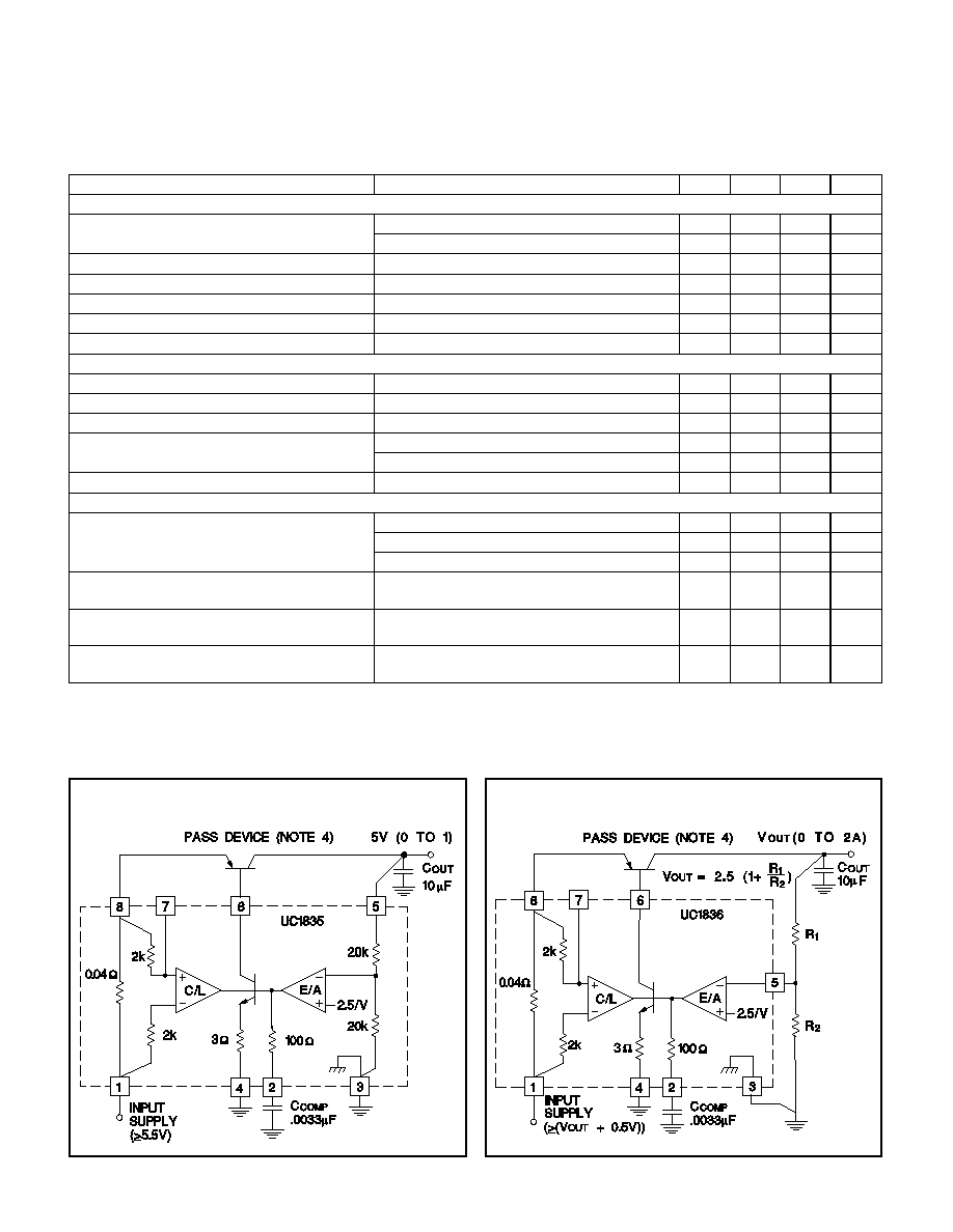
UC 1835
-
Typical configurations for a 2A,
Low Dropout 5V Regulator
UC1836
-
Typical Configuration for a 2A,
Low Dropout Adjustable Regulator
Note 4: Suggested Pass devices are TIP 32B. (Dropout Voltage
0.75V) or, D45H, (Dropout Voltage
0.5V), or equivalents.
APPLICATION AND OPERATION INFORMATION
3

UC1835 UC1836
UC2835 UC2836
UC3835 UC3836
EQUATIONS:
R
1
= 0.100 V/I
OUT
(MAX)
R
2
= (V
OUT
- 2.5V/1mA)
R
3
= ((V
IN
- V
BE
- V
SAT
)*BETA(min))/I
OUT
(max)
UC3835/36 TYPICAL APPLICATIONS
Low Current Application
using the UC3836 internal drive transistor
Typical Output Current vs V
IN
and V
OUT
of the UC3836 internal drive transistor
for P
DISS
= 0.5W (approx.)
High Current Application
using drive transistor Q
2
to increase Q
1
base drive
and reduce UC3836 power dissipation
Parallel Pass Transistors
can be added for high current or
high power dissipation applications
UNITRODE INTEGRATED CIRCUITS
7 CONTINENTAL BLVD.
∑
MERRIMACK, NH 03054
TEL. (603) 424-2410
∑
FAX 603-424-3460
APPLICATION AND OPERATION INFORMATION (cont.)
UC1835/6 Foldback Current Limiting
4

IMPORTANT NOTICE
Texas Instruments and its subsidiaries (TI) reserve the right to make changes to their products or to discontinue
any product or service without notice, and advise customers to obtain the latest version of relevant information
to verify, before placing orders, that information being relied on is current and complete. All products are sold
subject to the terms and conditions of sale supplied at the time of order acknowledgement, including those
pertaining to warranty, patent infringement, and limitation of liability.
TI warrants performance of its semiconductor products to the specifications applicable at the time of sale in
accordance with TI's standard warranty. Testing and other quality control techniques are utilized to the extent
TI deems necessary to support this warranty. Specific testing of all parameters of each device is not necessarily
performed, except those mandated by government requirements.
CERTAIN APPLICATIONS USING SEMICONDUCTOR PRODUCTS MAY INVOLVE POTENTIAL RISKS OF
DEATH, PERSONAL INJURY, OR SEVERE PROPERTY OR ENVIRONMENTAL DAMAGE ("CRITICAL
APPLICATIONS"). TI SEMICONDUCTOR PRODUCTS ARE NOT DESIGNED, AUTHORIZED, OR
WARRANTED TO BE SUITABLE FOR USE IN LIFE-SUPPORT DEVICES OR SYSTEMS OR OTHER
CRITICAL APPLICATIONS. INCLUSION OF TI PRODUCTS IN SUCH APPLICATIONS IS UNDERSTOOD TO
BE FULLY AT THE CUSTOMER'S RISK.
In order to minimize risks associated with the customer's applications, adequate design and operating
safeguards must be provided by the customer to minimize inherent or procedural hazards.
TI assumes no liability for applications assistance or customer product design. TI does not warrant or represent
that any license, either express or implied, is granted under any patent right, copyright, mask work right, or other
intellectual property right of TI covering or relating to any combination, machine, or process in which such
semiconductor products or services might be or are used. TI's publication of information regarding any third
party's products or services does not constitute TI's approval, warranty or endorsement thereof.
Copyright
©
1999, Texas Instruments Incorporated