 | –≠–ª–µ–∫—Ç—Ä–æ–Ω–Ω—ã–π –∫–æ–º–ø–æ–Ω–µ–Ω—Ç: UC1841J | –°–∫–∞—á–∞—Ç—å:  PDF PDF  ZIP ZIP |

UC1841
UC2841
UC3841
Programmable, Off-Line, PWM Controller
∑
All Control, Driving, Monitoring, and
Protection Functions Included
∑
Low-current, Off-line Start Circuit
∑
Voltage Feed Forward or Current
Mode Control
∑
Guaranteed Duty Cycle Clamp
∑
PWM Latch for Single Pulse per Period
∑
Pulse-by-Pulse Current Limiting Plus
Shutdown for Over-Current Fault
∑
No Start-up or Shutdown Transients
∑
Slow Turn-on Both Initially and After
Fault Shutdown
∑
Shutdown Upon Over- or
Under-Voltage Sensing
∑
Latch Off or Continuous Retry After
Fault
∑
PWM Output Switch Usable to 1A
Peak Current
∑
1% Reference Accuracy
∑
500kHz Operation
∑
18 Pin DIL Package
The UC1841 family of PWM controllers has been designed to increase
the level of versatility while retaining all of the performance features of
the earlier UC1840 devices. While still optimized for highly-efficient boot-
strapped primary-side operation in forward or flyback power converters,
the UC1841 is equally adept in implementing both low and high voltage
input DC to DC converters. Important performance features include a
low-current starting circuit, linear feed-forward for constant volt-second
operation, and compatibility with either voltage or current mode topologies.
In addition to start-up and normal regulating PWM functions, these de-
vices include built in protection from over-voltage, under-voltage, and
over-current fault conditions with the option for either latch-off or automat-
ic restart.
While pin compatible with the UC1840 in all respects except that the po-
larity of the External Stop has been reversed, the UC1841 offers the fol-
lowing improvements:
1. Fault latch reset is accomplished with slow start discharge rather
than recycling the input voltage to the chip.
2. The External Stop input can be used for a fault delay to resist
shutdown from short duration transients.
3. The duty-cycle clamping function has been characterized and
specified.
The UC1841 is characterized for -55∞C to +125∞C operation while the
UC2841 and UC3841 are designed for -25∞C to +85∞C and 0∞to +70∞C,
respectively.
BLOCK DIAGRAM
Note: Positive true logic, latch outputs high with set, reset has priority.
6/93
DESCRIPTION
FEATURES

PARAMETER
TEST CONDITIONS
UC1841 / UC2841
UC3841
UNITS
MIN
TYP
MAX
MIN
TYP
MAX
Power Inputs
Start-Up Current
V
IN
= 30V, Pin 2 = 2.5V
4.5
6
4.5
6
mA
Operating Current
V
IN
= 30V, Pin 2 = 3.5V
10
14
10
14
mA
Supply OV Clamp
I
IN
= 20mA
33
40
45
33
40
45
V
Reference Section
Reference Voltage
T
J
= 25∞C
4.95
5.0
5.05
4.9
5.0
5.1
V
Line Regulation
V
IN
= 8 to 30V
10
15
10
20
mV
Load Regulation
I
L
= 0 to 10mA
10
20
10
30
mV
Temperature Stability
Over Operating Temperature Range
4.9
5.1
4.85
5.15
V
Short Circuit Current
V
REF
= 0, T
J
= 25∞C
-80
-100
-80
-100
mA
Oscillator
Nominal Frequency
T
J
= 25∞C
47
50
53
45
50
55
kHz
Voltage Stability
V
IN
= 8 to 30V
0.5
1
0.5
1
%
Temperature Stability
Over Operating Temperature Range
45
55
43
57
kHz
Maximum Frequency
R
T
= 2k
, C
T
= 330pF
500
500
kHz
UC1841
UC2841
UC3841
ELECTRICAL CHARACTERISTICS:
Unless otherwise stated, these specifications apply for T
A
= -55∞C to +125∞C for the
UC1841, -25∞C to +85∞C for the UC2841, and 0∞C to +70∞C for the UC3841; V
IN
= 20V, R
T
= 20k
, C
T
= .001mfd, R
R
= 10k
,
C
R
= .001mfd, Current Limit Threshold = 200mV, T
A
= T
J.
Supply Voltage, +V
IN
(Pin 15) (Note 2)
Voltage Driven . . . . . . . . . . . . . . . . . . . . . . . . . . . . . . . . . +32V
Current Driven, 100mA maximum . . . . . . . . . . . . Self-limiting
PWM Output Voltage (Pin 12) . . . . . . . . . . . . . . . . . . . . . . . 40V
PWM Output Current, Steady-State (Pin 12) . . . . . . . . . 400mA
PWM Output Peak Energy Discharge . . . . . . . . . . . . 20
µ
Joules
Driver Bias Current (Pin 14) . . . . . . . . . . . . . . . . . . . . . -200mA
Reference Output Current (Pin 16) . . . . . . . . . . . . . . . . -50mA
Slow-Start Sink Current (Pin 8) . . . . . . . . . . . . . . . . . . . . 20mA
V
IN
Sense Current (Pin 11). . . . . . . . . . . . . . . . . . . . . . . . 10mA
Current Limit Inputs (Pins 6 & 7) . . . . . . . . . . . . . -0.5 to +5.5V
Stop Input (Pin 4) . . . . . . . . . . . . . . . . . . . . . . . . . -0.3 to +5.5V
Comparator Inputs
(Pins 1, 7, 9-11, 16) . . . . . . . . . . . . Internally clamped at 12V
Power Dissipation at T
A
= 25∞C (Note 3) . . . . . . . . . . . 1000mW
Power Dissipation at T
C
= 25∞C (Note 3) . . . . . . . . . . . 2000mW
Operating Junction Temperature . . . . . . . . . . -55∞C to +150∞C
Storage Temperature Range. . . . . . . . . . . . . . -65∞C to +150∞C
Lead Temperature (Soldering, 10 sec) . . . . . . . . . . . . . +300∞C
Note 1: All voltages are with respect to ground, Pin 13.
Currents are positive-into, negative-out of the specified
terminal.
Note 2: All pin numbers are referenced to DIL-18 package.
Note 3: Consult Packaging Section of Databook for thermal
limitations and considerations of package.
CONNECTION DIAGRAMS
PLCC-20, LCC-20
(TOP VIEW)
Q or L Package
DIL-18, SOIC-18 (TOP VIEW)
J or N, DW Package
PACKAGE PIN FUNCTIONS
FUNCTION
PIN
Comp
1
Start/UV
2
OV Sense
3
Stop
4
Reset
5
CUR Thresh
7
CUR Sense
8
Slow Start
9
R
T
/C
T
10
Ramp
11
V
IN
Sense
12
PWM Out
13
Ground
14
Drive Bias
15
+V
IN
Supply
17
5.0V REF
18
Inv. Input
19
N.I. Input
20
ABSOLUTE MAXIMUM RATINGS
2

PARAMETER
TEST CONDITIONS
UC1841 / UC2841
UC3841
UNITS
MIN
TYP
MAX
MIN
TYP
MAX
Ramp Generator
Ramp Current, Minimum
I
SENSE
= -10
µ
A
-11
-14
-11
-14
µ
A
Ramp Current, Maximum
I
SENSE
= 1.0mA
-0.9
-.95
-0.9
-.95
mA
Ramp Valley
0.3
0.4
0.6
0.3
0.4
0.6
V
Ramp Peak
Clamping Level
3.9
4.2
4.5
3.9
4.2
4.5
V
Error Amplifier
Input Offset Voltage
V
CM
= 5.0V
0.5
5
2
10
mV
Input Bias Current
0.5
2
1
5
µ
A
Input Offset Current
0.5
0.5
µ
A
Open Loop Gain
V
O
= 1 to 3V
60
66
60
66
dB
Output Swing (Max. Output
Ramp Peak - 100mV)
Minimum Total Range
0.3
3.5
0.3
3.5
V
CMRR
V
CM
= 1.5 to 5.5V
70
80
70
80
dB
PSRR
V
IN
= 8 to 30V
70
80
70
80
dB
Short Circuit Current
V
COMP
= 0V
-4
-10
-4
-10
mA
Gain Bandwidth*
T
J
= 25∞C, A
VOL
= 0dB
1
2
1
2
MHz
Slew Rate*
T
J
= 25∞C, A
VCL
= 0dB
0.8
0.8
V/
µ
s
PWM Section
Continuous Duty Cycle
Range* (other than zero)
Minimum Total Continuous Range,
Ramp Peak < 4.2V
4
95
4
95
%
50% Duty Cycle Clamp
R
SENSE
to V
REF
= 10k
42
47
52
42
47
52
%
Output Saturation
I
OUT
= 20mA
0.2
0.4
0.2
0.4
V
I
OUT
= 200mA
1.7
2.2
1.7
2.2
V
Output Leakage
V
OUT
= 40V
0.1
10
0.1
10
µ
A
Comparator Delay*
Pin 8 to Pin 12, T
J
= 25∞C, R
L
= 1k
300
500
300
500
ns
Sequencing Functions
Comparator Thresholds
Pins 2, 3, 5
2.8
3.0
3.2
2.8
3.0
3.2
V
Input Bias Current
Pins 3, 5 = 0V
-1.0
-4.0
-1.0
-4.0
µ
A
Input Leakage
Pins 3, 5 = 10V
0.1
2.0
0.1
2.0
µ
A
Start/UV Hysteresis Current
Pin 2 = 2.5V
170
200
220
170
200
230
µ
A
Ext. Stop Threshold
Pin 4
0.8
1.6
2.4
0.8
1.6
2.4
V
Error Latch Activate Current
Pin 4 = 0V, Pin 3 > 3V
-120
-200
-120
-200
µ
A
Driver Bias Saturation Voltage,
V
IN
- V
OH
I
B
= -50mA
2
3
2
3
V
Driver Bias Leakage
V
B
= 0V
-0.1
-10
-0.1
-10
µ
A
Slow-Start Saturation
I
S
= 10mA
0.2
0.5
0.2
0.5
V
Slow-Start Leakage
V
S
= 4.5V
0.1
2.0
0.1
2.0
µ
A
Current Control
Current Limit Offset
0
5
0
10
mV
Current Shutdown Offset
370
400
430
360
400
440
mV
Input Bias Current
Pin 7 = 0V
-2
-5
-2
-5
µ
A
Common Mode Range*
-0.4
3.0
-0.4
3.0
V
Current Limit Delay*
T
J
= 25∞C, Pin 7 to 12, R
L
= 1k
200
400
200
400
ns
* These parameters are guaranteed by design but not 100% tested in production.
UC1841
UC2841
UC3841
ELECTRICAL CHARACTERISTICS:
Unless otherwise stated, these specifications apply for T
A
= -55∞C to +125∞C for the
UC1841, -25∞C to +85∞C for the UC2841, and 0∞C to +70∞C for the UC3841; V
IN
= 20V, R
T
= 20k
, C
T
= .001mfd, R
R
= 10k
,
C
R
= .001mfd, Current Limit Threshold = 200mV, T
A
= T
J.
3

PWM CONTROL
1. Oscillator
Generates a fixed-frequency internal clock from an external R
T
and C
T
.
Frequency =
K
C
R
T
C
T
where K
C
is a first order correction factor
0.3 log (C
T
X 10
12
).
2. Ramp Generator
Develops a linear ramp with a slope defined externally by
dv
dt
=
sense
voltage
R
R
C
R
C
R
is normally selected
C
T
and its value will have some effect upon valley voltage.
Limiting the minimum value for I
SENSE
will establish a maximum duty cycle clamp.
C
R
terminal can be used as an input port for current mode control.
3. Error Amplifier
Conventional operational amplifier for closed-loop gain and phase compensation.
Low output impedance; unity-gain stable.
The output is held low by the slow start voltage at turn on in order to minimize overshoot.
4. Reference Generator
Precision 5.0V for internal and external usage to 50mA.
Tracking 3.0V reference for internal usage only with nominal accuracy of
±
2%.
40V clamp zener for chip OV protection, 100mA maximum current.
5. PWM Comparator
Generates output pulse which starts at termination of clock pulse and ends when the ramp
input crosses the lowest of two positive inputs.
6. PWM Latch
Terminates the PWM output pulse when set by inputs from either the PWM comparator, the
pulse-by-pulse current limit comparator, or the error latch. Resets with each internal clock
pulse.
7. PWM Output Switch
Transistor capable of sinking current to ground which is off during the PWM on-time and turns
on to terminate the power pulse. Current capacity is 400mA saturated with peak
capacitance discharge in excess of one amp.
SEQUENCING FUNCTIONS
1. Start/UV Sense
With an increasing voltage, it generates a turn-on signal and releases the slow-start clamp at
a
start
threshold.
With a decreasing voltage, it generates a turn-off command at a lower level separated by a
200
µ
A hysteresis current.
2. Drive Switch
Disables most of the chip to hold internal current consumption low, and Driver Bias OFF, until
input voltage reaches start threshold.
3. Driver Bias
Supplies drive current to external power switch to provide turn-on bias.
4. Slow Start
Clamps low to hold PWM OFF. Upon release, rises with rate controlled by R
S
C
S
for slow
increase of output pulse width.
Can also be used as an alternate maximum duty cycle clamp with an external voltage divider.
PROTECTION FUNCTIONS
1. Error Latch
When set by momentary input, this latch insures immediate PWM shutdown and hold off until
reset. Inputs to Error Latch are:
a. OV > 3.2V (typically 3V)
b. Stop > 2.4V (typically 1.6V)
c. Current Sense 400mV over threshold (typical).
Error Latch resets when slow start voltage falls to 0.4V if Reset Pin 5 < 2.8V. With Pin 5 >
3.2V, Error Latch will remain set.
2. Current Limiting
Differential input comparator terminates individual output pulses each time sense voltage
rises above threshold.
When sense voltage rises to 400mV (typical) above threshold, a shutdown signal is sent to
Error
Latch.
3. External Stop
A voltage over 1.2V will set the Error Latch and hold the output off.
A voltage less than 0.8V will defeat the error latch and prevent shutdown.
A capacitor here will slow the action of the error latch for transient protection by providing a
typical
delay
of
13ms/
µ
F.
UC1841
UC2841
UC3841
FUNCTIONAL DESCRIPTION
4

UC1841
UC2841
UC3841
Start/UV Hysteresis
PWM Output Minimum Pulse Width
Oscillator Frequency
PWM Output-Saturation Voltage
Shutdown Timing
Error Amplifier Open Loop Gain and Phase
5
FLYBACK APPLICATION (A)
In this application (see Figure A, next page), complete
control is maintained on the primary side. Control power
is provided by R
IN
and C
IN
during start-up, and by a pri-
mary-referenced low voltage winding, N2, for efficient op-
eration after start. The error amplifier loop is closed to
regulate the DC voltage from N2 with other outputs fol-
lowing through their magnetic coupling
-
a task made
even easier with the UC1841's feed
-
forward line regula-
tion.
An extension to this application for more precise regula-
tion would be the use of the UC1901 Isolated Feedback
Generator for direct closed-loop control to an output.
Not shown, are protective snubbers or additional interface
circuitry which may be required by the choice of the high-
voltage switch, Qs, or the application; however, one ex-
ample of power transistor interfacing is provided on the
following page.
REGULATOR APPLICATION (B)
With the addition of a level shifting transistor, Q1, the
UC1841 is an ideal control circuit for DC to DC converters
such as the buck regulator shown in Figure B opposite. In
addition to providing constant current drive pulses to the
PIC661 power switch, this circuit has full fault protection
and high speed dynamic line regulation due to its feed-
forward capability. An additional feature is the ability to
UC1841
UC2841
UC3841
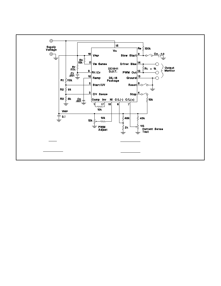
OPEN-LOOP TEST CIRCUIT
Nominal Frequency =
1
R
T
C
T
= 50 kHz
Start Voltage = 3
R1
+
R2
+
R3
R2
+
R3
+0.2R1 = 12V
UV Fault Voltage = 3
R1
+
R2
+
R3
R2
+
R3
= 8V
OV Fault Voltage = 3
R1
+
R2
+
R3
R3
= 32V
Current Limit = 200mV
Current Fault Voltage = 600mV
Duty Cycle Clamp = 50%
6

UC1841
UC2841
UC3841
Figure A.
UC1841 Programmable PWM Controller In A Simplified Flyback Regulator
Figure B.
Overall Schematic For A 300 Watt, Off-line Power Converter Using The UC3841 For Control
7
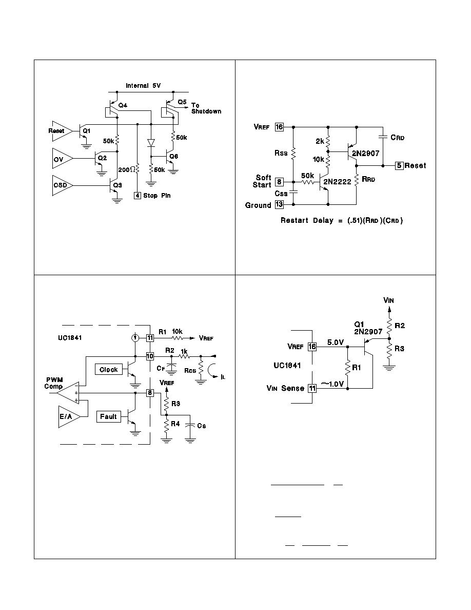
Since Pin 10 is a direct input to the PWM comparator, this
point can also serve as a current sense port for current mode
control. In this application, current sensing is ground refer-
enced through R
CS
. Resistor R1 sets a 400mV offset across
R2 (assuming R2 > R
CS
) so that both the Error Amplifier and
Fault Shutdown can force the current completely to zero. R2 is
also used along with C
F
as a small filter to attenuate leading-
edge spikes on the load current waveform. In this mode,
current limiting can be accomplished by divider R3/R4 which
forms a clamp overriding the output of the Error Amplifier.
In this circuit, R1 is used in conjunction with C
R
(not shown) to
establish a minimum ramp charging current such that the ramp
voltage reaches 4.2V at the required maximum output pulse
width.
The purpose of Q1 is to provide an increasing ramp current
above a threshold established by R2 and R3 such that the duty
cycle is further reduced with increasing V
IN
.
The minimum ramp current is:
l
R
(
MIN
)
=
V
REF
-
V
IN
SENSE
R
1
4
V
R
1
The threshold where V
IN
begins to add extra ramp current is:
V
IN
5.6V
R2
+
R3
R3
Above the threshold, the ramp current will be:
l
R
(
VARIAB
)
4
R1
+
V
IN
-
5.6
R2
-
5.6
R3
UC1841
UC2841
UC3841
ERROR LATCH INTERNAL CIRCUITRY
PROGRAMMABLE SOFT START AND
RESTART DELAY CIRCUIT
The Error Latch consists of Q5 and Q6 which, when both on,
turns off the PWM Output and pulls the Slow-Start pin low. This
latch is set by either the Over-Voltage or Current Shutdown
comparators, or by a high signal on Pin 4. Reset is accom-
plished by either the Reset comparator or a low signal on Pin
4. An activation time delay can be provided with an external
capacitor on Pin 4 in conjunction with the
100
µ
A collector
current from Q4.
UNITRODE INTEGRATED CIRCUITS
7 CONTINENTAL BLVD.
∑
MERRIMACK, NH 03054
TEL. (603) 424-2410
∑
FAX (603) 424-3460
VOLTAGE FEED-FORWARD COMBINED WITH
MAXIMUM DUTY-CYCLE CLAMP
CURRENT MODE CONTROL
8

IMPORTANT NOTICE
Texas Instruments and its subsidiaries (TI) reserve the right to make changes to their products or to discontinue
any product or service without notice, and advise customers to obtain the latest version of relevant information
to verify, before placing orders, that information being relied on is current and complete. All products are sold
subject to the terms and conditions of sale supplied at the time of order acknowledgement, including those
pertaining to warranty, patent infringement, and limitation of liability.
TI warrants performance of its semiconductor products to the specifications applicable at the time of sale in
accordance with TI's standard warranty. Testing and other quality control techniques are utilized to the extent
TI deems necessary to support this warranty. Specific testing of all parameters of each device is not necessarily
performed, except those mandated by government requirements.
CERTAIN APPLICATIONS USING SEMICONDUCTOR PRODUCTS MAY INVOLVE POTENTIAL RISKS OF
DEATH, PERSONAL INJURY, OR SEVERE PROPERTY OR ENVIRONMENTAL DAMAGE ("CRITICAL
APPLICATIONS"). TI SEMICONDUCTOR PRODUCTS ARE NOT DESIGNED, AUTHORIZED, OR
WARRANTED TO BE SUITABLE FOR USE IN LIFE-SUPPORT DEVICES OR SYSTEMS OR OTHER
CRITICAL APPLICATIONS. INCLUSION OF TI PRODUCTS IN SUCH APPLICATIONS IS UNDERSTOOD TO
BE FULLY AT THE CUSTOMER'S RISK.
In order to minimize risks associated with the customer's applications, adequate design and operating
safeguards must be provided by the customer to minimize inherent or procedural hazards.
TI assumes no liability for applications assistance or customer product design. TI does not warrant or represent
that any license, either express or implied, is granted under any patent right, copyright, mask work right, or other
intellectual property right of TI covering or relating to any combination, machine, or process in which such
semiconductor products or services might be or are used. TI's publication of information regarding any third
party's products or services does not constitute TI's approval, warranty or endorsement thereof.
Copyright
©
1999, Texas Instruments Incorporated