
UC1846/7
UC2846/7
UC3846/7
SLUS352A - JANUARY 1997 - REVISED MARCH 2002
∑
Automatic Feed Forward Compensation
∑
Programmable Pulse-by-Pulse Current
Limiting
∑
Automatic Symmetry Correction in Push-pull
Configuration
∑
Enhanced Load Response Characteristics
∑
Parallel Operation Capability for Modular
Power Systems
∑
Differential Current Sense Amplifier with
Wide Common Mode Range
∑
Double Pulse Suppression
∑
500mA (Peak) Totem-pole Outputs
∑
±1% Bandgap Reference
∑
Under-voltage Lockout
∑
Soft Start Capability
∑
Shutdown Terminal
∑
500kHZ Operation
Current Mode PWM Controller
The UC1846/7 family of control ICs provides all of the necessary
features to implement fixed frequency, current mode control
schemes while maintaining a minimum external parts count. The
superior performance of this technique can be measured in im-
proved line regulation, enhanced load response characteristics, and
a simpler, easier-to-design control loop. Topological advantages in-
clude inherent pulse-by-pulse current limiting capability, automatic
symmetry correction for push-pull converters, and the ability to par-
allel "power modules" while maintaining equal current sharing.
Protection circuitry includes built-in under-voltage lockout and pro-
grammable current limit in addition to soft start capability. A shut-
down function is also available which can initiate either a complete
shutdown with automatic restart or latch the supply off.
Other features include fully latched operation, double pulse sup-
pression, deadline adjust capability, and a
±1% trimmed bandgap
reference.
The UC1846 features low outputs in the OFF state, while the
UC1847 features high outputs in the OFF state.
BLOCK DIAGRAM
15
10
9
8
OSC
3
4
X3
+
5
6
E/A
7
COMP
INV
NI
C/S+
C/S-
CT
RT
SYNC
VIN
5.1 V
REFERENCE
REGULATOR
UVLO
LOCKOUT
2
VREF
13
11
VC
A OUT
14
12
B OUT
GND
Q
Q
T
S
S
R
Q
1
16
6 k
0.5 mA
350 mV
0.5 V
F/F
CURRENT
LIMIT ADJUST
SHUTDOWN
UC1846
Output Stage
UC1847
Output Inverted
COMP
FEATURES
DESCRIPTION
application
INFO
available
UDG-02057

2
UC1846/7
UC2846/7
UC3846/7
PACKAGE PIN FUNCTION
FUNCTION
PIN
N/C
1
C/L SS
2
V
REF
3
C/S-
4
C/S+
5
N/C
6
E/A+
7
E/A-
8
Comp
9
C
T
10
N/C
11
R
T
12
Sync
13
A Out
14
Gnd
15
N/C
16
V
C
17
B Out
18
V
IN
19
Shutdown
20
DIL-16, SOIC-16
(TOP VIEW)
J or N Package, DW Package
CONNECTION DIAGRAMS
ELECTRICAL CHARACTERISTICS
(Unless otherwise stated, these specifications apply for T
A
=-55∞C to +125∞C for
UC1846/7; -40∞C to +85∞C for the UC2846/7; and 0∞C to +70∞C for the UC3846/7;
V
IN
=15V, R
T
=10k, C
T
=4.7nF, T
A
=T
J
.)
UC1846/UC1847
UC3846/UC3847
PARAMETER
TEST CONDITIONS
UC2846/UC2847
MIN.
TYP.
MAX.
MIN.
TYP.
MAX. UNITS
Reference Section
Output Voltage
T
J
=25∞C, I
O
=1mA
5.05
5.10
5.15
5.00
5.10
5.20
V
Line Regulation
V
IN
=8V to 40V
5
20
5
20
mV
Load Regulation
I
L
=1mA to 10mA
3
15
3
15
mV
Temperature Stability
Over Operating Range, (Note 2)
0.4
0.4
mV/∞C
Total Output Variation
Line, Load, and Temperature (Note 2)
5.00
5.20
4.95
5.25
V
Output Noise Voltage
10Hz
f 10kHz, T
J
=25∞C (Note 2)
100
100
µV
Long Term Stability
T
J
=125∞C, 1000 Hrs. (Note 2)
5
5
mV
Short Circuit Output Current V
REF
=0V
-10
-45
-10
-45
mA
Supply Voltage (Pin 15) . . . . . . . . . . . . . . . . . . . . . . . . . . . . . . . . . . . . . . . . . +40V
Collector Supply Voltage (Pin 13) . . . . . . . . . . . . . . . . . . . . . . . . . . . . . . . . . +40V
Output Current, Source or Sink (Pins 11, 14) . . . . . . . . . . . . . . . . . . . . . . . 500mA
Analog Inputs (Pins 3, 4, 5, 6, 16). . . . . . . . . . . . . . . . . . . . . . . . . . . -0.3V to +V
IN
Reference Output Current (Pin 2) . . . . . . . . . . . . . . . . . . . . . . . . . . . . . . . . -30mA
Sync Output Current (Pin 10). . . . . . . . . . . . . . . . . . . . . . . . . . . . . . . . . . . . . -5mA
Error Amplifier Output Current (Pin 7) . . . . . . . . . . . . . . . . . . . . . . . . . . . . . . -5mA
Soft Start Sink Current (Pin 1). . . . . . . . . . . . . . . . . . . . . . . . . . . . . . . . . . . . 50mA
Oscillator Charging Current (Pin 9) . . . . . . . . . . . . . . . . . . . . . . . . . . . . . . . . . 5mA
Power Dissipation at T
A
=25∞C . . . . . . . . . . . . . . . . . . . . . . . . . . . . . . . . . 1000mW
Power Dissipation at T
C
=25∞C . . . . . . . . . . . . . . . . . . . . . . . . . . . . . . . . . 2000mW
Storage Temperature Range . . . . . . . . . . . . . . . . . . . . . . . . . . . . -65∞C to +150∞C
Lead Temperature (soldering, 10 seconds) . . . . . . . . . . . . . . . . . . . . . . . . +300∞C
ABSOLUTE MAXIMUM RATINGS (Note 1)
Note 1. All voltages are with respect to Ground, Pin 13. Currents are positive into,
negative out of the speficied terminal. Consult Packaging Section of Databook for
thermal limitations and considerations of packages. Pin numbers refer to DIL and
SOIC packages only.
PLCC-20, LCC-20
(TOP VIEW)
Q, L Packages

3
UC1846/7
UC2846/7
UC3846/7
UC1846/UC1847
UC3846/UC3847
PARAMETER
TEST CONDITIONS
UC2846/UC2847
MIN.
TYP.
MAX.
MIN.
TYP.
MAX. UNITS
Oscillator Section
Initial Accuracy
T
J
=25∞C
39
43
47
39
43
47
kHz
Voltage Stability
V
IN
=8V to 40V
-1
2
-1
2
%
Temperature Stability
Over Operating Range (Note 2)
-1
-1
%
Sync Output High Level
3.9
4.35
3.9
4.35
V
Sync Output Low Level
2.3
2.5
2.3
2.5
V
Sync Input High Level
Pin 8=0V
3.9
3.9
V
Sync Input Low Level
Pin 8=0V
2.5
2.5
V
Sync Input Current
Sync Voltage=3.9V, Pin 8=0V
1.3
1.5
1.3
1.5
mA
Error Amp Section
Input Offset Voltage
0.5
5
0.5
10
mV
Input Bias Current
-0.6
-1
-0.6
-2
µA
Input Offset Current
40
250
40
250
nA
Common Mode Range
V
IN
=8V to 40V
0
V
IN
-2V
0
V
IN
-2V
V
Open Loop Voltage Gain
V
O
=1.2 to 3V, V
CM
=2V
80
105
80
105
dB
Unity Gain Bandwidth
T
J
=25∞C (Note 2)
0.7
1.0
0.7
1.0
MHz
CMRR
V
CM
=0V to 38V, V
IN
=40V
75
100
75
100
dB
PSRR
V
IN
=8V to 40V
80
105
80
105
dB
Output Sink Current
V
ID
=-15mV to -5V, V
PIN 7
=1.2V
2
6
2
6
mA
Output Source Current
V
ID
=15mV to 5V, V
PIN 7
=2.5V
-0.4
-0.5
-0.4
-0.5
mA
High Level Output Voltage
R
L
=(Pin 7) 15k
4.3
4.6
4.3
4.6
V
Low Level Output Voltage
0.7
1
0.7
1
V
Current Sense Amplifier Section
Amplifier Gain
V
PIN 3
=0V, Pin 1 Open (Notes 3 & 4)
2.5
2.75
3.0
2.5
2.75
3.0
V
Maximum Differential Input
Pin 1 Open (Note 3)
Signal (V
PIN 4
-V
PIN 3
)
R
L
(Pin 7)=15kW
1.1
1.2
1.1
1.2
V
Input Offset Voltage
V
PIN 1
=0.5V, Pin 7 Open (Note 3)
5
25
5
25
mV
CMRR
V
CM
=1V to 12V
60
83
60
83
dB
PSRR
V
IN
=8V to 40V
60
84
60
84
dB
Input Bias Current
V
PIN 1
=0.5V, Pin 7 Open (Note 3)
-2.5
-10
-2.5
-10
µA
Input Offset Current
V
PIN 1
=0.5V, Pin 7 Open (Note 3)
0.08
1
0.08
1
µA
Input Common Mode Range
0
V
IN
-3
0
V
IN
-3
V
Delay to Outputs
T
J
=25∞C, (Note 2)
200
500
200
500
ns
Current Limit Adjust Section
Current Limit Offset
V
PIN 3
=0V, V
PIN 4
=0V, Pin 7 Open
(Note 3)
0.45
0.5
0.55
0.45
0.5
0.55
V
Input Bias Current
V
PIN 5
=V
REF
, V
PIN 6
=0V
-10
-30
-10
-30
µA
Shutdown Terminal Section
Threshold Voltage
250
350
400
250
350
400
mV
Input Voltage Range
0
V
IN
0
V
IN
V
Minimum Latching Current
(Note 6)
(I
PIN 1
)
3.0
1.5
3.0
1.5
mA
ELECTRICAL
CHARACTERISTICS (cont.)
(Unless otherwise stated, these specifications apply for T
A
=-55∞C to +125∞C for UC1846/7;
-40∞C to +85∞C for the UC2846/7; and 0∞C to +70∞C for the UC3846/7; V
IN
=15V, R
T
=10k,
C
T
=4.7nF, T
A
=T
J
.)
4
UC1846/7
UC2846/7
UC3846/7
Note 2. These parameters, although guaranteed over the recommended operating conditions, are not 100% tested in production.
Note 3. Parameter measured at trip point of latch with VPIN 5 = VREF, VPIN 6 = 0V.
Note 4. Amplifier gain defined as: G
V
V
PIN
PIN
=
7
4
;
V
PIN4
= 0 to 1.0V
Note 5. Applies to UC1846/UC2846/UC3846 only due to polarity of outputs.
Note 6. Current into Pin 1 guaranteed to latch circuit in shutdown state.
Note 7. Current into Pin 1 guaranteed not to latch circuit in shutdown state.
UC1846/UC1847
UC3846/UC3847
PARAMETER
TEST CONDITIONS
UC2846/UC2847
MIN.
TYP.
MAX.
MIN.
TYP.
MAX. UNITS
Shutdown Terminal Section (cont.)
Maximum Non-Latching
(Note 7)
Current (I
PIN 1
)
1.5
0.8
1.5
0.8
mA
Delay to Outputs
T
J
=25∞C (Note 2)
300
600
300
600
ns
Output Section
Collector-Emitter Voltage
40
40
V
Collector Leakage Current
V
C
=40V (Note 5)
200
200
µA
Output Low Level
I
SINK
=20mA
0.1
0.4
0.1
0.4
V
I
SINK
=100mA
0.4
2.1
0.4
2.1
V
Output High Level
I
SOURCE
=20mA
13
13.5
13
13.5
V
I
SOURCE
=100mA
12
13.5
12
13.5
V
Rise Time
C
L
=1nF, T
J
=25∞C (Note 2)
50
300
50
300
ns
Fall Time
C
L
=1nF, T
J
=25∞C (Note 2)
50
300
50
300
ns
Under-Voltage Lockout Section
Start-Up Threshold
7.7
8.0
7.7
8.0
V
Threshold Hysteresis
0.75
0.75
V
Total Standby Current
Supply Current
17
21
17
21
mA
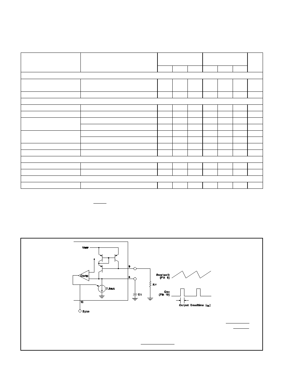
Oscillator Circuit
Output deadtime is determined by the external capacitor, C
T
, according to the formula:
µ
µ
d
s
T
f
(
)
(
)
=
145C
ID
ID -
3.6
RT (k )
.
For large values of R
T
:
µ
µ
d
s
T
f
(
)
(
)
145C
.
Oscillator frequency is approximated by the formula: fT kHz
RT k
CT
f
(
)
(
)
(
)
∑
2.2
µ
.
ELECTRICAL
CHARACTERISTICS (cont.)
(Unless otherwise stated, these specifications apply for T
A
=-55∞C to +125∞C for UC1846/7;
-40∞C to +85∞C for the UC2846/7; and 0∞C to +70∞C for the UC3846/7; V
IN
=15V, R
T
=10k,
C
T
=4.7nF, T
A
=T
J
.)
APPLICATIONS DATA
I
D
= Oscillator discharge current at 25∞C is typically 7.5.

5
UC1846/7
UC2846/7
UC3846/7
Error Amp Output Configuration
Error Amp Open-Logic D.C. Gain vs Load Resistance
Error Amp Gain and Phase vs Frequency
APPLICATIONS DATA (cont.)
Parallel Operation

6
UC1846/7
UC2846/7
UC3846/7
Pulse by Pulse Current Limiting
Soft Start and Shutdown /Restart Functions
Peak Current (I
S
) is determined by the formula: IS
R VREF
R
R
S
=
+
-
2
1
2
0.5
3R
APPLICATIONS DATA (cont.)

7
UC1846/7
UC2846/7
UC3846/7
Current Sense Amp Connection
UC1846 Open Loop Test Circuit
APPLICATIONS DATA (cont.)
A small RC filter may be required in some applications to reduce switch transients.
Differential input allows remote, noise free sensing.

IMPORTANT NOTICE
Texas Instruments Incorporated and its subsidiaries (TI) reserve the right to make corrections, modifications,
enhancements, improvements, and other changes to its products and services at any time and to discontinue
any product or service without notice. Customers should obtain the latest relevant information before placing
orders and should verify that such information is current and complete. All products are sold subject to TI's terms
and conditions of sale supplied at the time of order acknowledgment.
TI warrants performance of its hardware products to the specifications applicable at the time of sale in
accordance with TI's standard warranty. Testing and other quality control techniques are used to the extent TI
deems necessary to support this warranty. Except where mandated by government requirements, testing of all
parameters of each product is not necessarily performed.
TI assumes no liability for applications assistance or customer product design. Customers are responsible for
their products and applications using TI components. To minimize the risks associated with customer products
and applications, customers should provide adequate design and operating safeguards.
TI does not warrant or represent that any license, either express or implied, is granted under any TI patent right,
copyright, mask work right, or other TI intellectual property right relating to any combination, machine, or process
in which TI products or services are used. Information published by TI regarding third≠party products or services
does not constitute a license from TI to use such products or services or a warranty or endorsement thereof.
Use of such information may require a license from a third party under the patents or other intellectual property
of the third party, or a license from TI under the patents or other intellectual property of TI.
Reproduction of information in TI data books or data sheets is permissible only if reproduction is without
alteration and is accompanied by all associated warranties, conditions, limitations, and notices. Reproduction
of this information with alteration is an unfair and deceptive business practice. TI is not responsible or liable for
such altered documentation.
Resale of TI products or services with statements different from or beyond the parameters stated by TI for that
product or service voids all express and any implied warranties for the associated TI product or service and
is an unfair and deceptive business practice. TI is not responsible or liable for any such statements.
Mailing Address:
Texas Instruments
Post Office Box 655303
Dallas, Texas 75265
Copyright
2002, Texas Instruments Incorporated