 | –≠–ª–µ–∫—Ç—Ä–æ–Ω–Ω—ã–π –∫–æ–º–ø–æ–Ω–µ–Ω—Ç: UC1901J | –°–∫–∞—á–∞—Ç—å:  PDF PDF  ZIP ZIP |
Document Outline
- Application Notes
- Design Notes
UC1901
UC2901
UC3901
Isolated Feedback Generator
FEATURES
∑
An Amplitude-Modulation System for
Transformer Coupling an Isolated
Feedback Error Signal
∑
Low-Cost Alternative to Optical
Couplers
∑
Internal 1% Reference and Error
Amplifier
∑
Internal Carrier Oscillator Usable to
5MHz
∑
Modulator Synchronizable to an
External Clock
∑
Loop Status Monitor
DESCRIPTION
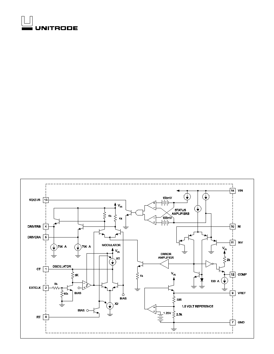
The UC1901 family is designed to solve many of the problems associ-
ated with closing a feedback control loop across a voltage isolation
boundary. As a stable and reliable alternative to an optical coupler, these
devices feature an amplitude modulation system which allows a loop er-
ror signal to be coupled with a small RF transformer or capacitor.
The programmable, high-frequency oscillator within the UC1901 series
permits the use of smaller, less expensive transformers which can readily
be built to meet the isolation requirements of today's line-operated power
systems. As an alternative to RF operation, the external clock input to
these devices allows synchronization to a system clock or to the switch-
ing frequency of a SMPS.
An additional feature is a status monitoring circuit which provides an active-
low output when the sensed error voltage is within
±
10% of the reference.
The DRIVERA output, DRIVERB output, and STATUS output are disabled
until the input supply has reached a sufficient level to allow proper operation
of the device.
Since these devices can also be used as a DC driver for optical couplers,
the benefits of 4.5 to 40V supply operation, a 1% accurate reference, and a
high gain general purpose amplifier offer advantages even though an AC
system may not be desired.
µ
µ
µ
UC1901 SIMPLIFIED SCHEMATIC
11/98
UDG-98080

2
UC1901
UC2901
UC3901
ABSOLUTE MAXIMUM RATINGS
(Note 1)
Input Supply Voltage, V
IN
. . . . . . . . . . . . . . . . . . . . . . . . . . 40V
Reference Output Current . . . . . . . . . . . . . . . . . . . . . . . ≠10mA
Driver Output Currents . . . . . . . . . . . . . . . . . . . . . . . . . . ≠35mA
Status Indicator Voltage . . . . . . . . . . . . . . . . . . . . . . . . . . . 40V
Status Indicator Current . . . . . . . . . . . . . . . . . . . . . . . . . . 20mA
Ext. Clock Input . . . . . . . . . . . . . . . . . . . . . . . . . . . . . . . . . . 40V
Error Amplifier Inputs . . . . . . . . . . . . . . . . . . . . . ≠0.5V to +35V
Power Dissipation at T
A
= 25∞C . . . . . . . . . . . . . . . . . . 1000mW
Power Dissipation at T
C
= 25∞C . . . . . . . . . . . . . . . . . 2000mW
Operating Junction Temperature . . . . . . . . . . ≠55∞C to +150∞C
Storage Temperature . . . . . . . . . . . . . . . . . . . ≠65∞C to +150∞C
Lead Temperature (Soldering, 10 seconds) . . . . . . . . . . 300∞C
Note 1: Voltages are referenced to ground, Pin 7. Currents are
positive into, negative out of the specified terminal.
Note 2: Consult Packaging section of Databook for thermal limi-
tations and considerations of package.
CONNECTION DIAGRAMS
DIL-14, SOIC-14 (TOP VIEW)
J or N Package, D Package
PLCC-20, LCC-20 (TOP VIEW)
Q, L Packages
SOIC-16 Wide (TOP VIEW)
DW Package
TEMPERATURE
RANGE
AVAILABLE
PACKAGES
UC1901
≠55∞C to +125∞C
J, L
UC2901
≠40∞C to +85∞C
D, DW, J, N, Q
UC3901
0∞C to +70∞C
D, DW, J, N, Q
TEMPERATURE AND PACKAGE SELECTION
GUIDE
3
UC1901
UC2901
UC3901
ELECTRICAL CHARACTERISTICS
Unless otherwise stated, these specifications apply for V
IN
= 10V, R
T
= 10k
, C
T
=
820pF, T
A
= T
J.
PARAMETER
TEST CONDITIONS
UC1901/UC2901
UC3901
UNITS
MIN
TYP
MAX
MIN
TYP
MAX
Reference Section
Output Voltage
T
J
= 25∞C
1.485
1.5
1.515
1.47
1.5
1.53
V
T
MIN
T
J
T
MAX
1.470
1.5
1.530
1.455
1.5
1.545
Line Regulation
V
IN
= 4.5 to 35V
2
10
2
15
mV
Load Regulation
I
OUT
= 0 to 5mA
4
10
4
15
mV
Short Circuit Current
T
J
= 25∞C
≠35
≠55
≠35
≠55
mV
Error Amplifier Section (To Compensation Terminal)
Input Offset Voltage
V
CM
= 1.5V
1
4
1
8
mV
Input Bias Current
V
CM
= 1.5V
≠1
≠3
≠1
≠6
µ
A
Input Offset Current
V
CM
= 1.5V
0.1
1
0.1
2
µ
A
Small Signal Open Loop Gain
40
60
40
60
dB
CMRR
V
CM
= 0.5 to 7.5V
60
80
60
80
dB
PSRR
V
IN
= 2 to 25V
80
100
80
100
dB
Output Swing,
V
O
0.4
0.7
0.4
0.7
V
Maximum Sink Current
90
150
90
150
µ
A
Maximum Source Current
≠2
≠3
≠2
≠3
mA
Gain Band Width Product
1
1
MHz
Slew Rate
0.3
0.3
V/
µ
S
Modulators/Drivers Section (From Compensation Terminal)
Voltage Gain
11
12
13
10
12
14
dB
Output Swing
±
1.6
±
2.8
±
1.6
±
2.8
V
Driver Sink Current
500
700
500
700
µ
A
Driver Source Current
≠15
≠35
≠15
≠35
mA
Gain Band Width Product
25
25
MHz
Oscillator Section
Initial Accuracy
T
J
= 25∞C
140
150
160
130
150
170
kHz
T
MIN
T
J
T
MAX
130
170
120
180
kHz
Line Sensitivity
V
IN
= 5 to 35V
.15
.35
.15
.60
%/V
Maximum Frequency
R
T
= 10k, C
T
= 10pF
5
5
MHz
Ext. Clock Low Threshold
Pin 1 (C
T
) = V
IN
0.5
0.5
V
Ext. Clock High Threshold
Pin 1 (C
T
) = V
IN
1.6
1.6
V
Status Indicator Section
Input Voltage Window
@ E/A Inputs, V
CM
= 1.5V
±
135
±
150
±
165
±
130
±
150
±
170
mV
Saturation Voltage
E/A
Input = 0V, I
SINK
= 1.6mA
0.45
0.45
V
Max. Output Current
Pin 13 = 3V, E/A
Input = 0.0V
8
15
8
15
mA
Leakage Current
Pin 13 = 40V, E/A
Input = 0.2V
.05
1
.05
5
µ
A
Supply Current
V
IN
= 35V
5
8
5
10
mA
UVLO Section
Drivers Enabled Threshold
At Input Supply V
IN
3.9
4.5
3.9
4.5
V
Status Output Enabled
Threshold
At Input Supply V
IN
3.9
4.5
3.9
4.5
V
Change in Reference Output
When V
IN
Reaches UVLO
Threshold
≠2
≠30
≠2
≠30
mV
4
UC1901
UC2901
UC3901
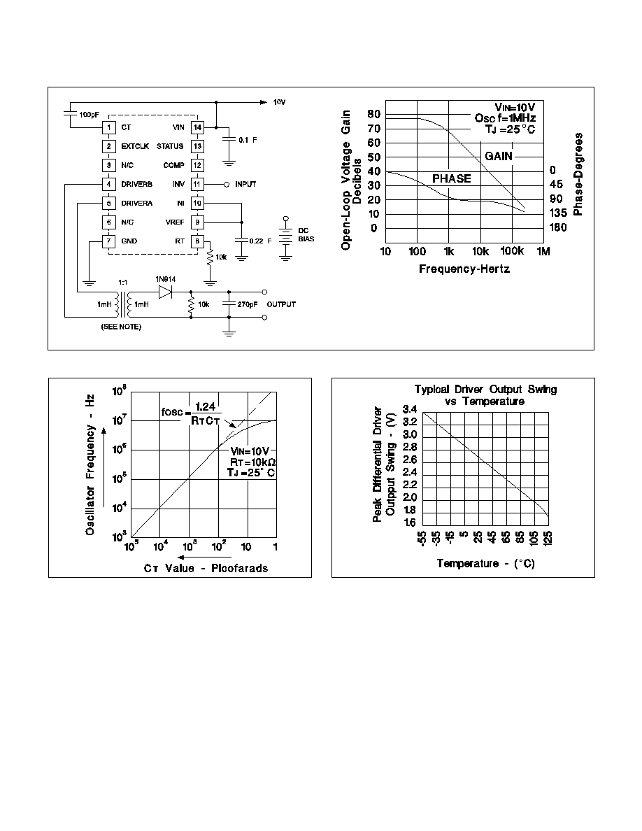
Figure 1. Transformer Coupled Open Loop Transfer Function
µ
µ
Note:
Transformer Data: N1 = N2 = 20TAWG 26
Core = Ferroxcube 3E2A Ferrite, 0.5" O.D. toroid
Carrier Frequency = 1MHz
Figure 2. Oscillator Frequency
Figure 3. Typical Driver Output Swing vs
Temperature
The error amplifier compensation terminal, Pin 12, is in-
tended as a source of feedback to the amplifier's invert-
ing input at Pin 11. For most applications, a series DC
blocking capacitor should be part of the feedback net-
work. The amplifier is internally compensated for unity
feedback.
The waveform at the driver outputs is a squarewave with
an amplitude that is proportional to the error amplifier in-
put signal. There is a fixed 12dB of gain from the error
amplifier compensation pin to the modulator driver out-
puts. The frequency of the output waveform is controlled
by either the internal oscillator or an external clock signal.
With the internal oscillator the squarewave will have a
fixed 50% duty cycle. If the internal oscillator is disabled
by connecting Pin 1, C
R
, to V
IN
then the frequency and
duty cycle of the output will be determined by the input
clock waveform at Pin 2. If the oscillator remains disabled
and there is not clock input at Pin 2, there will be a linear
12dB of signal gain to one or the other of the driver out-
puts depending on the DC state of Pin 2.
The driver outputs are emitter followers which will source
a minimum of 15mA of current. The sink current, inter-
nally limited at 700
µ
A, can be increased by adding resis-
tors to ground at the driver outputs.
APPLICATION INFORMATION
5
UC1901
UC2901
UC3901
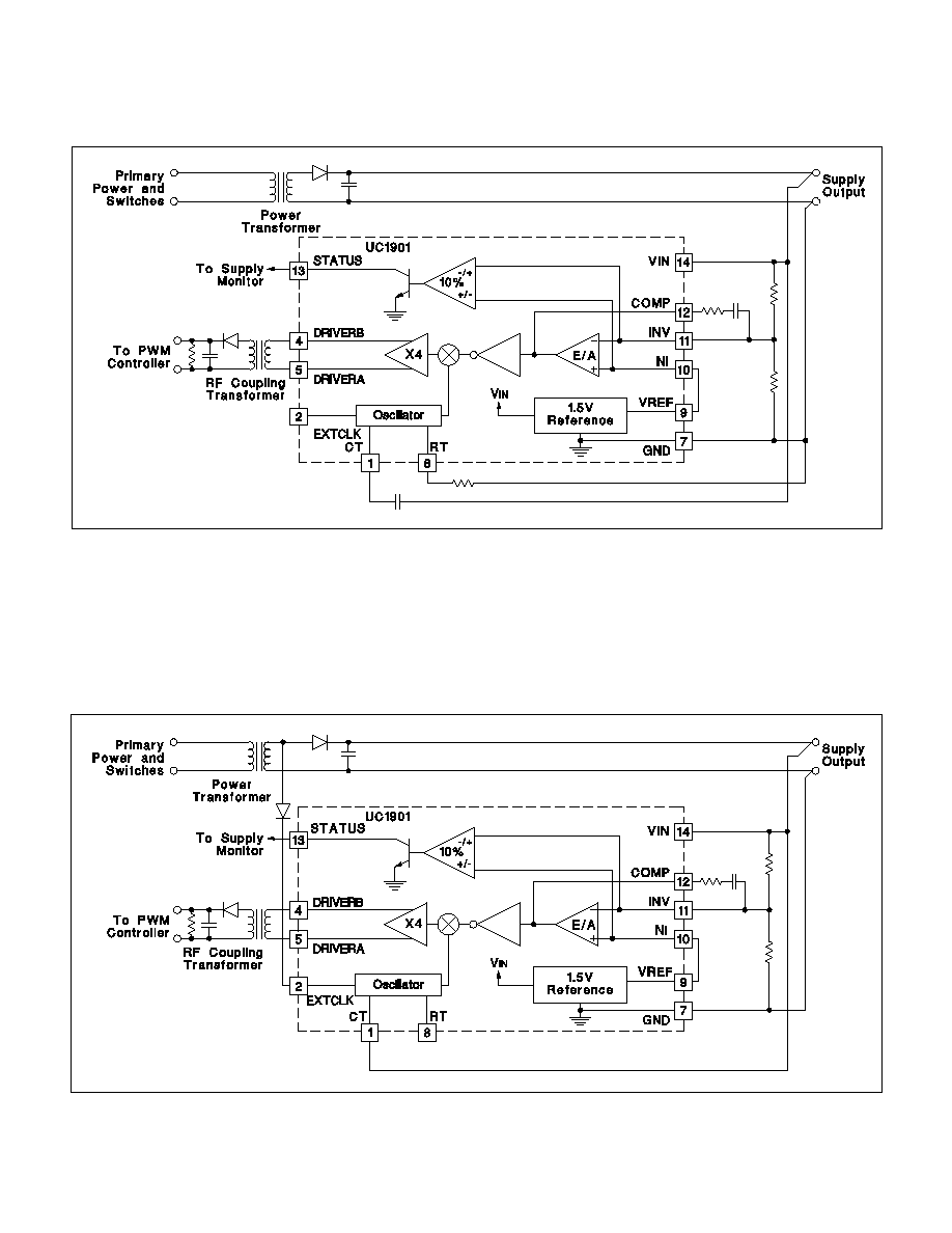
Figure 4. R.F. Transformer Coupled Feedback
APPLICATION INFORMATION (continued)
Figure 5. Feedback Coupled at Switching Frequency

6
UC1901
UC2901
UC3901
UNITRODE CORPORATION
7 CONTINENTAL BLVD. ∑ MERRIMACK, NH 03054
TEL. (603) 424-2410 ∑ FAX (603) 424-3460
Figure 6. Optically Coupled DC Feedback
TYPICAL APPLICATION
UDG-98196

IMPORTANT NOTICE
Texas Instruments and its subsidiaries (TI) reserve the right to make changes to their products or to discontinue
any product or service without notice, and advise customers to obtain the latest version of relevant information
to verify, before placing orders, that information being relied on is current and complete. All products are sold
subject to the terms and conditions of sale supplied at the time of order acknowledgement, including those
pertaining to warranty, patent infringement, and limitation of liability.
TI warrants performance of its semiconductor products to the specifications applicable at the time of sale in
accordance with TI's standard warranty. Testing and other quality control techniques are utilized to the extent
TI deems necessary to support this warranty. Specific testing of all parameters of each device is not necessarily
performed, except those mandated by government requirements.
CERTAIN APPLICATIONS USING SEMICONDUCTOR PRODUCTS MAY INVOLVE POTENTIAL RISKS OF
DEATH, PERSONAL INJURY, OR SEVERE PROPERTY OR ENVIRONMENTAL DAMAGE ("CRITICAL
APPLICATIONS"). TI SEMICONDUCTOR PRODUCTS ARE NOT DESIGNED, AUTHORIZED, OR
WARRANTED TO BE SUITABLE FOR USE IN LIFE-SUPPORT DEVICES OR SYSTEMS OR OTHER
CRITICAL APPLICATIONS. INCLUSION OF TI PRODUCTS IN SUCH APPLICATIONS IS UNDERSTOOD TO
BE FULLY AT THE CUSTOMER'S RISK.
In order to minimize risks associated with the customer's applications, adequate design and operating
safeguards must be provided by the customer to minimize inherent or procedural hazards.
TI assumes no liability for applications assistance or customer product design. TI does not warrant or represent
that any license, either express or implied, is granted under any patent right, copyright, mask work right, or other
intellectual property right of TI covering or relating to any combination, machine, or process in which such
semiconductor products or services might be or are used. TI's publication of information regarding any third
party's products or services does not constitute TI's approval, warranty or endorsement thereof.
Copyright
©
1999, Texas Instruments Incorporated