Simple Step-Up Voltage Regulator
∑
Requires Few External Components
∑
NPN Output Switches 3.0A, 65V(max)
∑
Extended Input Voltage Range: 3.0V to 40V
∑
Current Mode Operation for Improved
Transient Response, Line Regulation, and
Current Limiting
∑
Soft Start Function Provides Controlled
Startup
∑
52kHz Internal Oscillator
∑
Output Switch Protected by Current Limit,
Undervoltage Lockout and Thermal
Shutdown
∑
Improved Replacement for LM2577-ADJ
Series
The UC2577-ADJ device provides all the active functions neces-
sary to implement step-up (boost), flyback, and forward converter
switching regulators. Requiring only a few components, these sim-
ple regulators efficiently provide up to 60V as a step-up regulator,
and even higher voltages as a flyback or forward converter regula-
tor.
The UC2577-ADJ features a wide input voltage range of 3.0V to
40V and an adjustable output voltage. An on-chip 3.0A NPN switch
is included with undervoltage lockout, thermal protection circuitry,
and current limiting, as well as soft start mode operation to reduce
current during startup. Other features include a 52kHz fixed fre-
quency on-chip oscillator with no external components and current
mode control for better line and load regulation.
A standard series of inductors and capacitors are available from
several manufacturers optimized for use with these regulators and
are listed in this data sheet.
UC2577-ADJ
3/97
FEATURES
DESCRIPTION
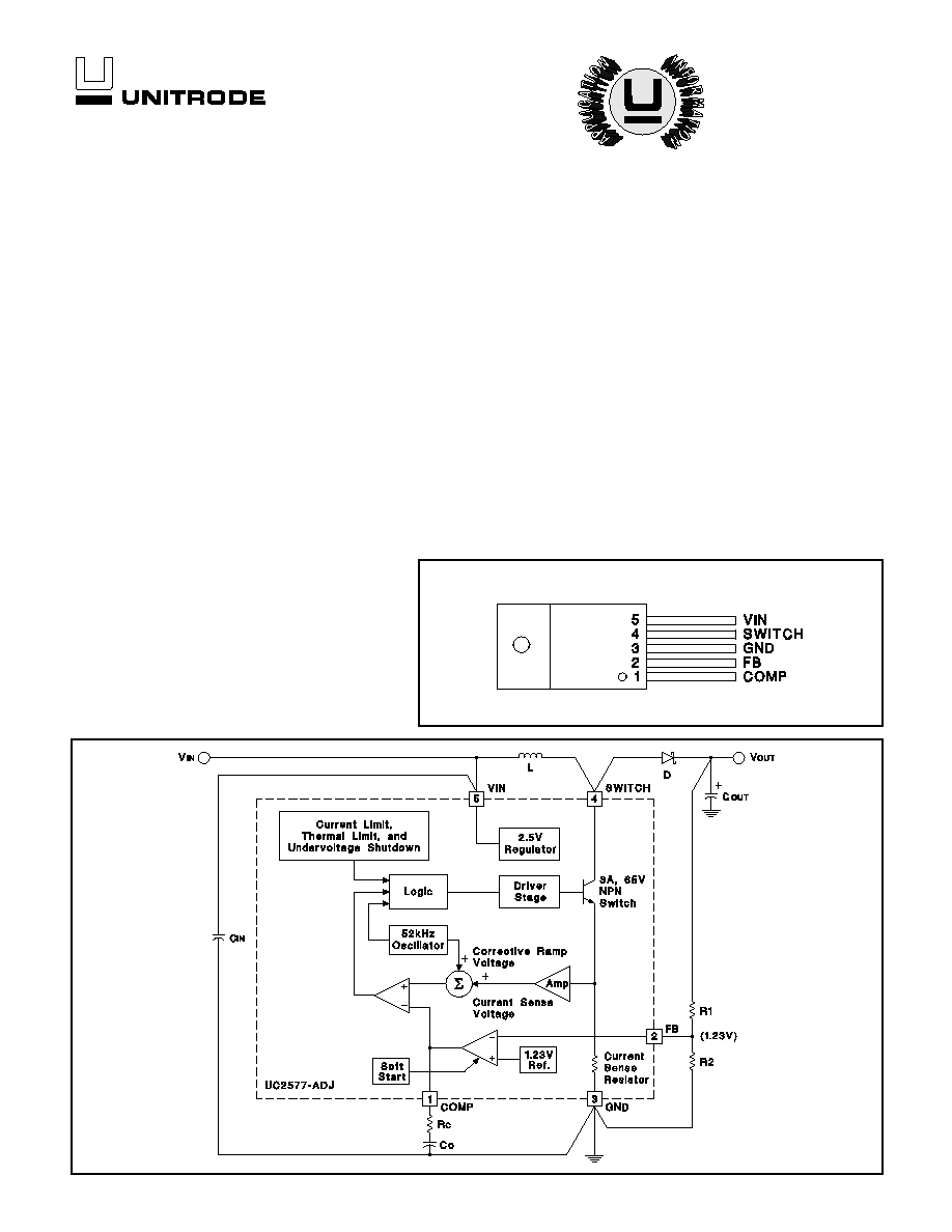
CONNECTION DIAGRAM
BLOCK DIAGRAM
UDG-94034
∑
Simple Boost and Flyback Converters
∑
SEPIC Topology Permits Input Voltage to
be Higher or Lower than Output Voltage
∑
Transformer Coupled Forward Regulators
∑
Multiple Output Designs
TYPICAL APPLICATIONS
5-Pin TO-220 (Top View)
Also available in TO-263 Package.

PARAMETER
TEST CONDITIONS
MIN
TYP
MAX
UNITS
System Parameters
Circuit Figure 1 (Note 3)
Output Voltage
VIN = 5V to 10V, I
LOAD
= 100mA to 800mA
11.40
12.0
12.60
V
T
J
= 25
∞
C
11.60
12.40
V
Line Regulation
VIN = 3.0V to 10V, I
LOAD
= 300mA
20
100
mV
T
J
= 25
∞
C
50
mV
Load Regulation
VIN = 5V, I
LOAD
= 100mA to 800mA
20
100
mV
T
J
= 25
∞
C
50
mV
Efficiency
VIN = 5V, I
LOAD
= 800mA
80
%
Device Parameters
Input Supply Current
V
FB
= 1.5V (Switch Off)
7.5
14
mA
T
J
= 25
∞
C
10
mA
I
SWITCH
= 2.0A, V
COMP
= 2.0V (Max Duty Cycle)
45
85
mA
T
J
= 25
∞
C
70
mA
Input Supply UVLO
I
SWITCH
= 100mA
2.70
2.95
V
T
J
= 25
∞
C
2.85
V
Oscillator Frequency
Measured at SWITCH Pin, I
SWITCH
= 100mA
42
52
62
kHz
T
J
= 25
∞
C
48
56
kHz
Reference Voltage
Measured at FB Pin, VIN = 3.0V to 40V, V
COMP
= 1.0V
1.206
1.230
1.254
V
T
J
= 25
∞
C
1.214
1.246
V
Reference Voltage Line Regulation
VIN = 3.0V to 40V
0.5
mV
Error Amp Input Bias Current
V
COMP
= 1.0V
100
800
nA
T
J
= 25
∞
C
300
nA
Error Amp Transconductance
I
COMP
=
-
30
µ
A to +30
µ
A, V
COMP
= 1.0V
1600
3700
5800
µ
mho
T
J
= 25
∞
C
2400
4800
µ
mho
Error Amp Voltage Gain
V
COMP
= 0.8V to 1.6V, R
COMP
= 1.0MW (Note 4)
250
800
V/V
T
J
= 25
∞
C
500
V/V
Error Amplifier Output Swing
Upper Limit V
FB
= 1.0V
2.0
2.4
V
T
J
= 25
∞
C
2.2
V
Lower Limit V
FB
= 1.5V
0.3
0.55
V
T
J
= 25
∞
C
0.40
V
Error Amp Output Current
V
FB
= 1.0V to 1.5V, V
COMP
= 1.0V
±
90
±
200
±
400
µ
A
T
J
= 25
∞
C
±
130
±
300
µ
A
Soft Start Current
V
FB
= 1.0V, V
COMP
= 0.5V
1.5
5.0
9.5
µ
A
T
J
= 25
∞
C
2.5
7.5
µ
A
Maximum Duty Cycle
V
COMP
= 1.5V, I
SWITCH
= 100mA
90
95
%
T
J
= 25
∞
C
93
%
Unless otherwise stated, these specifications apply for T
A
=
-
40
∞
C
to
+125
∞
C, VIN =
5V, V
FB
= V
REF
, I
SWITCH
= 0, and T
A
=T
J
.
ELECTRICAL CHARACTERISTICS
RECOMMENDED OPERATING RANGE
Supply Voltage . . . . . . . . . . . . . . . . . . . . . . . . . . . . . . . . . . . 45V
Output Switch Voltage . . . . . . . . . . . . . . . . . . . . . . . . . . . . . 65V
Output Switch Current (Note 2) . . . . . . . . . . . . . . . . . . . . . 6.0A
Power Dissipation . . . . . . . . . . . . . . . . . . . . . . Internally Limited
Storage Temperature Range . . . . . . . . . . . . .
-
65
∞
C to +150
∞
C
Lead Temperature (Soldering, 10 sec.) . . . . . . . . . . . . . . 260
∞
C
Maximum Junction Temperature . . . . . . . . . . . . . . . . . . . 150
∞
C
Minimum ESD Rating (C = 100pF, R = 15k
) . . . . . . . . . . . 2kV
ABSOLUTE MAXIMUM RATINGS (Note 1)
UC2577-ADJ
Supply Voltage . . . . . . . . . . . . . . . . . . . . . . . . 3.0V
VIN
40V
Output Switch Voltage . . . . . . . . . . . . . . . 0V
V
SWITCH
60V
Output Switch Current . . . . . . . . . . . . . . . . . . . . I
SWITCH
3.0A
Junction Temperature Range . . . . . . . . . .
-
40
∞
C
T
J
+125
∞
C
2
UC2577-ADJ
PARAMETER
TEST CONDITIONS
MIN
TYP
MAX
UNITS
Device Parameters (cont.)
Switch Transconductance
12.5
A/V
Switch Leakage Current
V
SWITCH
= 65V, V
FB
= 1.5V (Switch Off)
10
600
µ
A
T
J
= 25
∞
C
300
µ
A
Switch Saturation Voltage
I
SWITCH
= 2.0A, V
COMP
= 2.0V (Max Duty Cycle)
0.5
0.9
V
T
J = 25
∞
C
0.7
V
NPN Switch Current Limit
V
COMP
= 2.0V
3.0
4.3
6.0
A
Thermal Resistance
Junction to Ambient
65
∞
C/W
Junction to Case
2
∞
C/W
COMP Pin Current
V
COMP
= 0
25
50
µ
A
T
J
= 25
∞
C
40
µ
A
Unless otherwise stated, these specifications apply for T
A
=
-
40
∞
C
to
+125
∞
C, VIN =
5V, V
FB
= V
REF
, I
SWITCH
= 0, and T
A
=T
J
.
ELECTRICAL CHARACTERISTICS
Note 1: Absolute Maximum Ratings indicate limits beyond which damage to the device may occur. Operating ratings
indicate conditions during which the device is intended to be functional, but device parameter specifications may not be
guaranteed under these conditions. For guaranteed specifications and test conditions, see the Electrical Characteristics.
Note 2: Output current cannot be internally limited when the UC2577 is used as a step-up regulator. To prevent damage to
the switch, its current must be externally limited to 6.0A. However, output current is internally limited when the UC2577 is
used as a flyback or forward converter regulator.
Note 3. External components such as the diode, inductor, input and output capacitors can affect switching regulator
performance. When the UC2577 is used as shown in the Test Circuit, system performance will be as specified by the
system parameters.
Note 4: A 1.0M
resistor is connected to the compensation pin (which is the error amplifier's output) to ensure accuracy in
measuring A
VOL.
In actual applications, this pin's load resistance should be
10M
, resulting in A
VOL
that is typically twice
the guaranteed minimum limit.
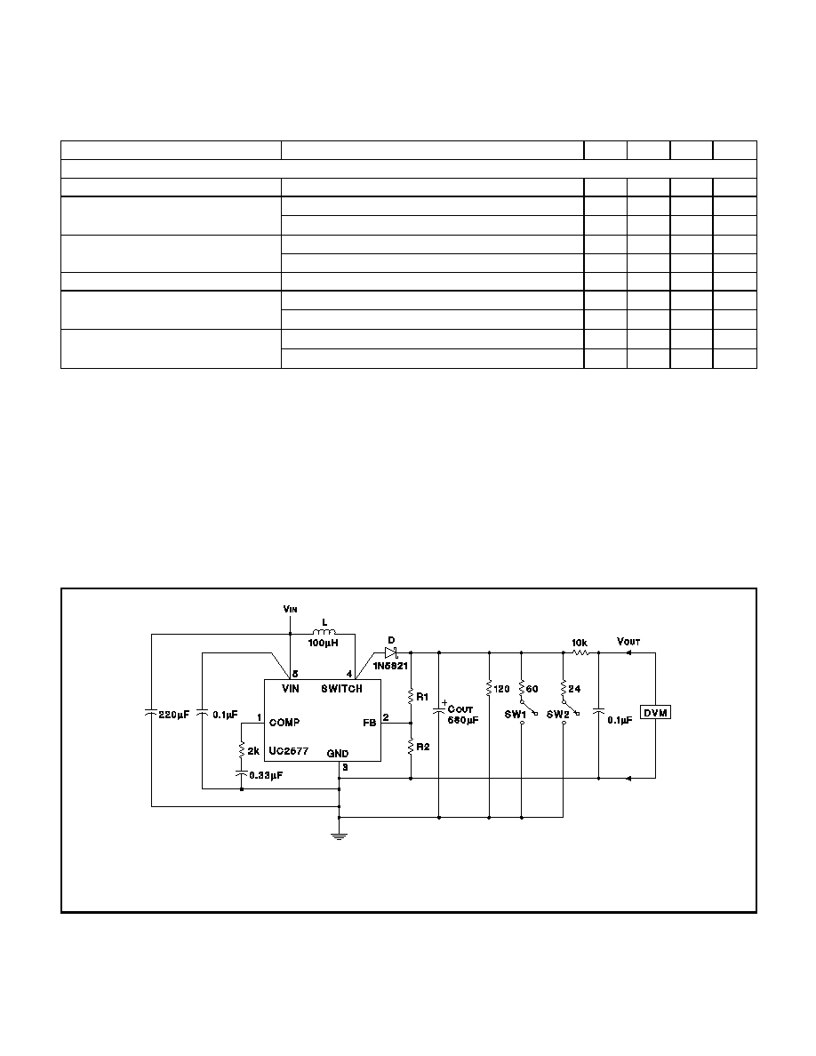
Figure 1. Circuit Used to Specify System Parameters
UDG-94035
L = 415-0930 (AIE)
D = any manufacturer
C
OUT
= Sprague Type 673D
Electrolytic 680
µ
F, 20V
R1 = 48.7k in series with 511
(1%)
R2 = 5.62k (1%)
3
The Block Diagram shows a step-up switching regulator
utilizing the UC2577. The regulator produces an output
voltage higher than the input voltage. The UC2577 turns
its switch on and off at a fixed frequency of 52kHz, thus
storing energy in the inductor (L). When the NPN switch
is on, the inductor current is charged at a rate of VIN/L.
When the switch is off, the voltage at the SWITCH termi-
nal of the inductor rises above VIN, discharging the
stored current through the output diode (D) into the out-
put capacitor (C
OUT
) at a rate of (V
OUT
- VIN)/L. The en-
ergy stored in the inductor is thus transferred to the
output.
The output voltage is controlled by the amount of energy
transferred, which is controlled by modulating the peak
inductor current. This modulation is accomplished by
feeding a portion of the output voltage to an error ampli-
fier which amplifies the difference between the feedback
voltage and an internal 1.23V precision reference volt-
age. The output of the error amplifier is then compared to
a voltage proportional to the switch current, or the induc-
tor current, during the switch on time. A comparator ter-
minates the switch on time when the two voltages are
equal and thus controls the peak switch current to main-
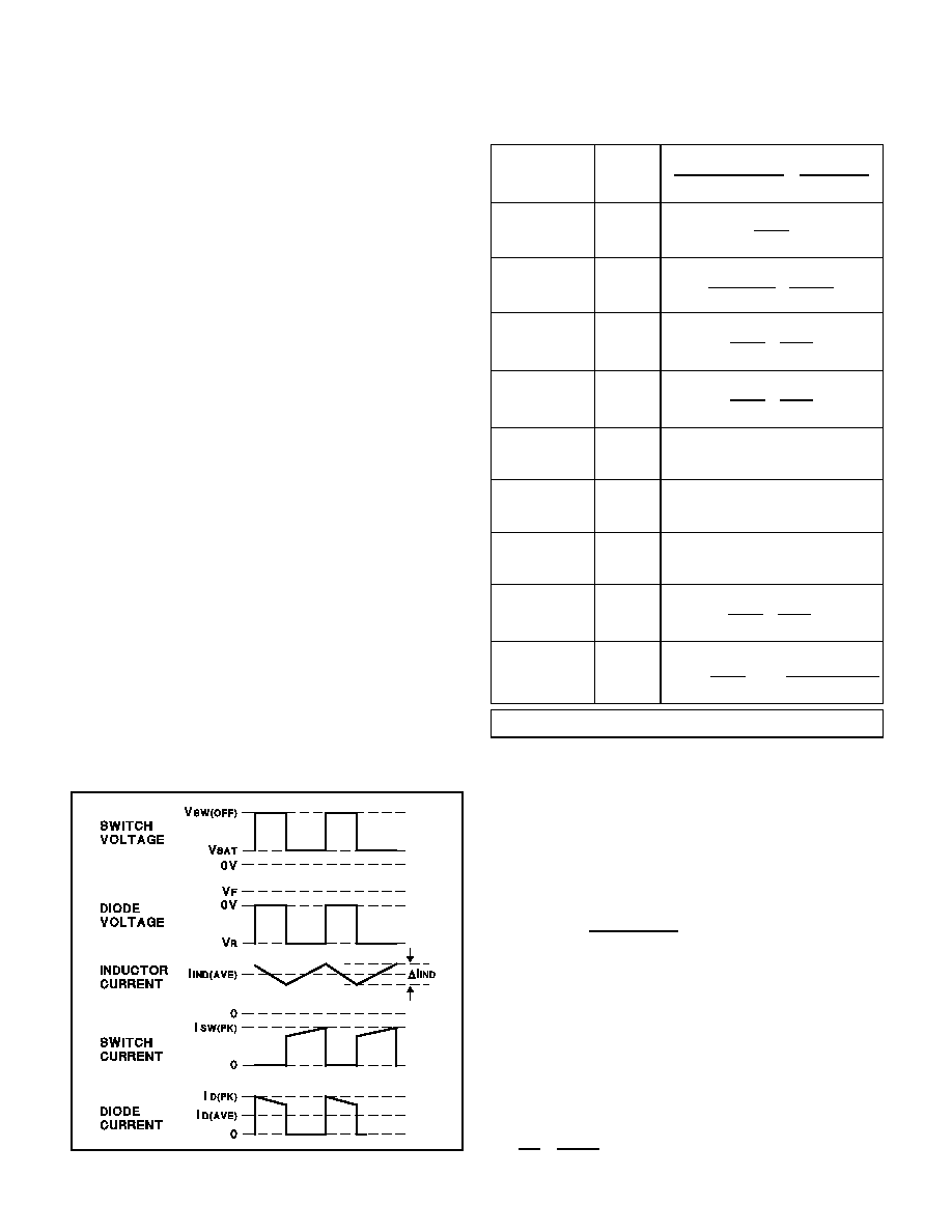
tain a constant output voltage. Figure 2 shows voltage
and current waveforms for the circuit. Formulas for calcu-
lation are shown in Figure 3.
STEP-UP REGULATOR DESIGN PROCEDURE
Refer to the Block Diagram
Given:
V
INmin
= Minimum input supply voltage
V
OUT
= Regulated output voltage
UC2577-ADJ
Step-up (Boost) Regulator
Duty Cycle
D
V
OUT
+
V
F
-
V
IN
V
OUT
+
V
F
-
V
SAT
V
OUT
-
V
IN
V
OUT
Avg. Inductor
Current
I
IND(AVG)
I
LOAD
1
-
D
Inductor
Current Ripple
I
IND
V
IN
-
V
SAT
L
∑
D
52,000
Peak Inductor
Current
I
IND(PK)
I
LOAD
1
-
D
+
I
IND
2
Peak Switch
Current
I
SW(PK)
I
LOAD
1
-
D
+
I
IND
2
Switch Voltage
when Off
V
SW(OFF)
V
OUT
+ V
F
Diode Reverse
Voltage
V
R
V
OUT
- V
SAT
Avg. Diode
Current
I
D(AVG)
I
LOAD
Peak Diode
Current
I
D(PK)
I
LOAD
1
-
D
+
I
IND
2
.
Power
Dissipation
P
D
0.25
I
LOAD
1
-
D
2
D
+
I
LOAD
∑
D
∑
V
IN
50
(
1
-
D
)
V
F
= Forward Biased Diode Voltage, I
LOAD
= Output Load
Figure 2. Step-up Regulator Waveforms
First, determine if the UC2577 can provide these values
of V
OUT
and I
LOADmax
when operating with the minimum
value of V
IN
. The upper limits for V
OUT
and I
LOADmax
are
given by the following equations.
V
OUT
60V and
V
OUT
10
∑
V
INmin
I
LOADmax
2.1A
∑
V
INmin
V
OUT
These limits must be greater than or equal to the values
specified in this application.
1. Output Voltage Section
Resistors R1 and R2 are used to select the desired out-
put voltage. These resistors form a voltage divider and
present a portion of the output voltage to the error ampli-
fier which compares it to an internal 1.23V reference. Se-
lect R1 and R2 such that:
R1
R2
=
V
OUT
1.23V
-
1
Figure 3. Step-up Regulator Formulas
APPLICATIONS INFORMATION
4
2. Inductor Selection (L)
A. Preliminary Calculations
To select the inductor, the calculation of the following
three parameters is necessary:
Dmax, the maximum switch duty cycle (0
D
0.9):
D
max
=
V
OUT
+
V
F
-
V
INmin
V
OUT
+
V
F
-
0.6V
where typically V
F
= 0.5V for Schottky diodes and V
F
=
0.8V for fast recovery diodes.
E
∑
T, the product of volts
∑
time that charges the induc-
tor:
E
∑
T
=
D
max
∑
(
V
INmin
-
0.6V
)
10
6
52,000Hz
(
V
∑
µ
s
)
I
IND, DC
, the average inductor current under full load:
I
IND,
DC
=
1.05
∑
I
LOADmax
1
-
D
max
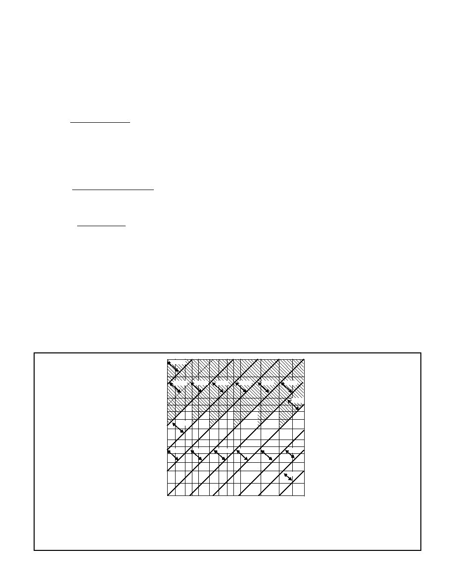
B. Identify Inductor Value:
1. From Figure 4, identify the inductor code for the region
indicated by the intersection of E
∑
T and I
IND, DC
. This
code gives the inductor value in microhenries. The L or H
prefix signifies whether the inductor is rated for a maxi-
mum E
∑
T of 90V
µ
s (L) or 250V
µ
s (H).
2. If D < 0.85, go to step C. If D
0.85, calculate the
minimum inductance needed to ensure the switching
regulator's stability:
0.3
0.4 0.45
0.35
0.5 0.6 0.7 0.8 0.9 1.0
1.5
2.0
2.5
3.0
20
30
35
25
40
45
50
60
70
80
90
100
200
150
L47
L68
L100
L150
L220
L330
H2200
L680
H1500
H1000
H680
H470
H330
H220
H150
L470
E∑T (V∑
µ
s)
I
IND, DC
(A)
Figure 4. Inductor Selection Graph
If L
min
is smaller than the inductor values found in step
B1, go on to step C. Otherwise, the inductor value found
in step B1 is too low; an appropriate inductor code
should be obtained from the graph as follows:
1.
Find the lowest value inductor that is greater than
L
min
.
2.
Find where E
∑
T intersects this inductor value to
determine if it has an L or H prefix. If E
∑
T intersects
both the L and H regions, select the inductor with an
H prefix.
C.
Inductor Selection
Select an inductor from the table of Figure 5 which cross
references the inductor codes to the part numbers of the
three different manufacturers. The inductors listed in this
table have the following characteristics:
AIE
(ferrite, pot-core inductors): Benefits of this type
are low etectromagnetic interference (EMI), small
physical size, and very low power dissipation (core
loss).
Pulse
(powdered iron, toroid core inductors): Bene-
fits are low EMI and ability to withstand E
∑
T and
peak current above rated value better than ferrite
cores.
Renco
(ferrite, bobbin-core inductors): Benefits are
low cost and best ability to withstand E
∑
T and peak
current above rated value. Be aware that these in-
ductors generate more EMI than the other types, and
this may interfere with signals sensitive to noise.
UC2577-ADJ
Note: This chart assumes that the inductor ripple current inductor is approximately 20% to 30% of the average inductor current
(when the regulator is under full load). Greater ripple current causes higher peak switch currents and greater output ripple volt-
age. Lower ripple current is achieved with larger value inductors. The factor of 20% to 30% is chosen as a convenient balance
between the two extremes.
APPLICATIONS INFORMATION (cont.)
5

UC2577-ADJ
3. Compensation Network (R
C
, C
C
) and Output
Capacitor (C
OUT
) Selection
The compensation network consists of resistor R
C
and
capacitor C
C
which form a simple pole-zero network and
stabilize the regulator. The values of R
C
and C
C
depend
upon the voltage gain of the regulator, I
LOADmax
, the in-
ductor L, and output capacitance C
OUT
. A procedure to
calculate and select the values for R
C
, C
C,
and C
OUT
which ensures stability is described below. It should be
noted, however, that this may not result in optimum com-
pensation. To guarantee optimum compensation a stand-
ard procedure for testing loop stability is recommended,
such as measuring V
OUT
transient responses to pulsing
I
LOAD
.
A. Calculate the maximum value for R
C
.
R
C
750
∑
I
LOADmax
∑
V
OUT
2
V
INmin
2
Select a resistor less than or equal to this value, not to
exceed 3k
.
B. Calculate the minimum value for C
OUT
using the fol-
lowing two equations.
C
OUT
0.19
∑
L
∑
R
C
∑
I
LOADmax
V
INmin
∑
V
OUT
and
C
OUT
V
INmin
∑
R
C
∑
(
V
INmin
+
(
3.74
∑
10
5
∑
L
))
487,800
∑
V
OUT
3
The larger of these two values is the minimum value that
ensures stability.
C. Calculate the minimum value of C
C
.
C
C
58.5
∑
V
OUT
2
∑
C
OUT
R
C
2
∑
V
INmin
The compensation capacitor is also used in the soft start
function of the regulator. When the input voltage is ap-
plied to the part, the switch duty cycle is increased slowly
at a rate defined by the compensation capacitor and the
soft start current, thus eliminating high input currents.
Without the soft start circuitry, the switch duty cycle would
instantly rise to about 90% and draw large currents from
the input supply. For proper soft starting, the value for C
C
should be equal or greater than 0.22
µ
F.
Figure 6 lists several types of aluminum electrolytic ca-
pacitors which could be used for the output filter. Use the
following parameters to select the capacitor.
Working Voltage (WVDC):
Choose a capacitor with a
working voltage at least 20% higher than the regulator
output voltage.
Ripple Current:
This is the maximum RMS value of cur-
rent that charges the capacitor during each switching cy-
cle. For step-up and flyback regulators, the formula for
ripple current is:
I
RIPPLErms
=
I
LOADmax
∑
D
max
1
-
D
max
Choose a capacitor that is rated at least 50% higher than
this value at 52kHz.
Equivalent Series Resistance (ESR):
This is the primary
cause of output ripple voltage, and it also affects the val-
ues of R
C
and C
C
needed to stabilize the regulator. As a
result, the preceding calculations for C
C
and R
C
are only
valid if the ESR does not exceed the maximum value
specified by the following equations.
ESR
0.01
∑
15V
I
RIPPLE
(
P
-
P
)
and
8.7
∑
10
-
3
∑
V
IN
I
LOADmax
where
I
RIPPLE
(
P
-
P
)
=
1.15
∑
I
LOADmax
1
-
D
max
Select a capacitor with an ESR, at 52kHz, that is less
than or equal to the lower value calculated. Most electro-
lytic capacitors specify ESR at 120kHz which is 15% to
30% higher than at 52kHz. Also, note that ESR increases
by a factor of 2 when operating at
-
20
∞
C.
In general, low values of ESR are achieved by using
large value capacitors (C
470
µ
F), and capacitors with
high WVDC, or by paralleling smaller value capacitors.
Inductor
Code
Manufacturer's Part Number
AIE
Pulse
Renco
L47
415 - 0932
PE - 53112
RL2442
L68
415 - 0931
PE - 92114
RL2443
L100
415 - 0930
PE - 92108
RL2444
L150
415 - 0953
PE - 53113
RL1954
L220
415 - 0922
PE - 52626
RL1953
L330
415 - 0926
PE - 52627
RL1952
L470
415 - 0927
PE - 53114
RL1951
L680
415 - 0928
PE - 52629
RL1950
H150
415 - 0936
PE - 53115
RL2445
H220
430 - 0636
PE - 53116
RL2446
H330
430 - 0635
PE - 53117
RL2447
H470
430 - 0634
PE - 53118
RL1961
H680
415 - 0935
PE - 53119
RL1960
H1000
415 - 0934
PE - 53120
RL1959
H1500
415 - 0933
PE - 53121
RL1958
H2200
415 - 0945
PE - 53122
RL2448
AIE Magnetics, Div. Vernitron Corp., (813)347-2181
2801 72nd Street North, St. Petersburg, FL 33710
Pulse Engineering, (619)674-8100
12220 World Trade Drive, San Diego, CA 92128
Renco Electronics, Inc., (516)586-5566
60 Jeffryn Blvd. East, Deer Park, NY 11729
Figure 5. Table of Standardized Inductors and
Manufacturer's Part Numbers
APPLICATIONS INFORMATION (cont.)
6

UNITRODE CORPORATION
7 CONTINENTAL BLVD.
∑
MERRIMACK, NH 03054
TEL. (603) 424-2410
∑
FAX (603) 424-3460
4. Input Capacitor Selection (C
IN
)
To reduce noise on the supply voltage caused by the
switching action of a step-up regulator (ripple current
noise), VIN should be bypassed to ground. A good qual-
ity 0.1
µ
F capacitor with low ESR should provide suffi-
cient decoupling. If the UC2577 is located far from the
supply source filter capacitors, an additional electrolytic
(47
µ
F, for example) is required.
Nichicon - Types PF, PX, or PZ
927 East StateParkway, Schaumburg, IL 60173
(708)843-7500
United Chemi-CON - Types LX, SXF, or SXJ
9801 West Higgens, Rosemont, IL 60018
(708)696-2000
Figure 6. Aluminum Electrolytic Capacitors Recommended
for Switching Regulators
5. Output Diode Selection (D)
In the step-up regulator, the switching diode must with-
stand a reverse voltage and be able to conduct the peak
output current of the UC2577. Therefore a suitable diode
must have a minimum reverse breakdown voltage
greater than the circuit output voltage, and should also
be rated for average and peak current greater than
I
LOADmax
and I
Dpk
. Because of their low forward voltage
drop (and thus higher regulator efficiencies), Schottky
barrier diodes are often used in switching regulators. Re-
fer to Figure 7 for recommended part numbers and volt-
age ratings of 1A and 3A diodes.
V
OUTmax
Schottky
Fast Recovery
1A
3A
1A
3A
20V
1N5817
1N5820
MBR120P MBR320P
30V
1N5818
1N5821
MBR130P MBR330P
11DQ03
31DQ03
40V
1N5819
1N5822
MBR140P MBR340P
11DQ04
31DQ04
50V
MBR150
MBR350
1N4933
11DQ05
31DQ05
MUR105
100V
1N4934
MR851
MUR110
30DL1
10DL1
MR831
MBRxxx and MURxxx are manufactured by Motorola.
1DDxxx, 11Cxx and 31Dxx are manufactured by
International Rectifier
Figure 7. Diode Selection Chart
UC2577-ADJ
ORDERING INFORMATION
Unitrode Type Number
UC2577T
KC-ADJ 5 Pin TO-220 Plastic Pkg -50 pc Tube
UC2577TDKTTT-ADJ 5 Pin TO-263 Plastic Pkg -50 pc Reel
APPLICATIONS INFORMATION (cont.)
7
UC2577TDTR-ADJ 5 Pin TO-263 Plastic Pkg -500 pc Reel

IMPORTANT NOTICE
Texas Instruments and its subsidiaries (TI) reserve the right to make changes to their products or to discontinue
any product or service without notice, and advise customers to obtain the latest version of relevant information
to verify, before placing orders, that information being relied on is current and complete. All products are sold
subject to the terms and conditions of sale supplied at the time of order acknowledgement, including those
pertaining to warranty, patent infringement, and limitation of liability.
TI warrants performance of its semiconductor products to the specifications applicable at the time of sale in
accordance with TI's standard warranty. Testing and other quality control techniques are utilized to the extent
TI deems necessary to support this warranty. Specific testing of all parameters of each device is not necessarily
performed, except those mandated by government requirements.
CERTAIN APPLICATIONS USING SEMICONDUCTOR PRODUCTS MAY INVOLVE POTENTIAL RISKS OF
DEATH, PERSONAL INJURY, OR SEVERE PROPERTY OR ENVIRONMENTAL DAMAGE ("CRITICAL
APPLICATIONS"). TI SEMICONDUCTOR PRODUCTS ARE NOT DESIGNED, AUTHORIZED, OR
WARRANTED TO BE SUITABLE FOR USE IN LIFE-SUPPORT DEVICES OR SYSTEMS OR OTHER
CRITICAL APPLICATIONS. INCLUSION OF TI PRODUCTS IN SUCH APPLICATIONS IS UNDERSTOOD TO
BE FULLY AT THE CUSTOMER'S RISK.
In order to minimize risks associated with the customer's applications, adequate design and operating
safeguards must be provided by the customer to minimize inherent or procedural hazards.
TI assumes no liability for applications assistance or customer product design. TI does not warrant or represent
that any license, either express or implied, is granted under any patent right, copyright, mask work right, or other
intellectual property right of TI covering or relating to any combination, machine, or process in which such
semiconductor products or services might be or are used. TI's publication of information regarding any third
party's products or services does not constitute TI's approval, warranty or endorsement thereof.
Copyright
©
1999, Texas Instruments Incorporated