 | –≠–ª–µ–∫—Ç—Ä–æ–Ω–Ω—ã–π –∫–æ–º–ø–æ–Ω–µ–Ω—Ç: UC2625 | –°–∫–∞—á–∞—Ç—å:  PDF PDF  ZIP ZIP |
UC1625
UC2625
UC3625
SLUS353A - NOVEMBER 1999
Brushless DC Motor Controller
FEATURES
∑ Drives Power MOSFETs or Power Darlingtons
Directly
∑ 50V Open Collector High-Side Drivers
∑ Latched Soft Start
∑ High-speed Current-Sense Amplifier with Ideal
Diode
∑ Pulse-by-Pulse and Average Current Sensing
∑ Over-Voltage and Under-Voltage Protection
∑ Direction Latch for Safe Direction Reversal
∑ Tachometer
∑ Trimmed Reference Sources 30mA
∑ Programmable Cross-Conduction Protection
∑ Two-Quadrant and Four-Quadrant Operation
DESCRIPTION
The UC3625 family of motor controller ICs integrate most of the
functions required for high-performance brushless DC motor con-
trol into one package.
When coupled with external power
MOSFETs or Darlingtons, these ICs perform fixed-frequency PWM
motor control in either voltage or current mode while implementing
closed loop speed control and braking with smart noise rejection,
safe direction reversal, and cross≠conduction protection.
Although specified for operation from power supplies between 10V
and 18V, the UC1625 can control higher voltage power devices
with external level-shifting components. The UC1625 contains fast,
high-current push-pull drivers for low-side power devices and 50V
open-collector outputs for high-side power devices or level shifting
circuitry.
The UC1625 is characterized for operation over the military tem-
perature range of ≠55
∞C to +125∞C, while the UC2625 is charac-
terized from ≠40
∞C to +105∞C and the UC3625 is characterized
from 0
∞C to 70∞C.
(NOTE: ESD Protection to 2kV)
application
INFO
available
UDG-99045
21
27
25
22
6
28
1
15
24
3
26
10k
3k
10k
2
19
20
16
11
20
µF
100nF
20
µF
100nF
+
R
OSC
33k
2200pF
C
OSC
68k
R
T
3nF
C
T
BRAKE
5nF
100nF
23
8
9
10
4
5
7
2nF
2nF
2nF
100nF
10k
5nF
240
240
17
18
14
13
12
3k
2N3906
100nF
1k
4k
TO OTHER
CHANNELS
TO OTHER
CHANNELS
10
2N3904
10
IRF9350
IRF532
3k
FROM
HALL
SENSORS
VMOTOR
+15V
+5V TO HALL
SENSORS
VREF
0.02
R
S
TO
MOTOR
0.02
R
D
REQUIRED
FOR
AVERAGE
CURRENT
SENSING
REQUIRED
FOR BRAKE
AND FAST
REVERSE
100
µF
+
UC3625
DIR
QUAD
TYPICAL APPLICATION
2
UC1625
UC2625
UC3625
V
CC
Supply Voltage . . . . . . . . . . . . . . . . . . . . . . . . . . . . . . +20V
Pwr V
CC
Supply Voltage . . . . . . . . . . . . . . . . . . . . . . . . . . +20V
PWM In . . . . . . . . . . . . . . . . . . . . . . . . . . . . . . . . . . . ≠0.3 to 6V
E/A IN(+), E/A IN(≠) . . . . . . . . . . . . . . . . . . . . . . . . . ≠0.3 to 12V
I
SENSE1
, I
SENSE2
. . . . . . . . . . . . . . . . . . . . . . . . . . . . . ≠1.3 to 6V
OV≠Coast, Dir, Speed-In, S
START
, Quad Sel . . . . . . ≠0.3 to 8V
H1, H2, H3 . . . . . . . . . . . . . . . . . . . . . . . . . . . . . . . . ≠0.3 to 12V
PU Output Voltage. . . . . . . . . . . . . . . . . . . . . . . . . . ≠0.3 to 50V
PU Output Current . . . . . . . . . . . . . . . . . . +200 mA continuous
PD Output Current . . . . . . . . . . . . . . . . . .
±200 mA continuous
E/A Output Current . . . . . . . . . . . . . . . . . . . . . . . . . . . .
±10 mA
I
SENSE
Output Current . . . . . . . . . . . . . . . . . . . . . . . . . . ≠10 mA
Tach Out Output Current . . . . . . . . . . . . . . . . . . . . . . . .
±10 mA
V
REF
Output Current . . . . . . . . . . . . . . . . . . ≠50 mA continuous
Operating Temperature Range UC1625. . . . . . ≠55∞C to 125∞C
Operating Temperature Range UC2625. . . . . . ≠40∞C to 105∞C
Operating Temperature Range UC3625. . . . . . . . . 0∞C to 70∞C
Note 1: Currents are positive into and negative out of the spec-
ified terminal.
Note 2: Consult Unitrode Integrated Circuits databook for infor-
mation regarding thermal specifications and limitations
of packages.
ABSOLUTE MAXIMUM RATINGS
ELECTRICAL CHARACTERISTICS: Unless otherwise stated, these specifications apply for: T
A
= 25
∞C; Pwr V
CC
= V
CC
= 12V;
R
OSC =
20k to V
REF
; C
OSC
= 2nF; R
TACH
= 33k; C
TACH
= 10nF; and all outputs unloaded. T
A
= T
J.
PARAMETER
TEST CONDITIONS
MIN
TYP
MAX
UNITS
Overall
Supply current
Over Operating Range
14.5
30.0
mA
V
CC
Turn-On Threshold
Over Operating Range
8.65
8.95
9.45
V
V
CC
Turn-Off Threshold
Over Operating Range
7.75
8.05
8.55
V
Overvoltage/Coast
OV-Coast Inhibit Threshold
Over Operating Range
1.65
1.75
1.85
V
OV-Coast Restart Threshold
1.55
1.65
1.75
V
OV-Coast Hysteresis
0.05
0.10
0.15
V
OV-Coast Input Current
≠10
≠1
0
µA
Logic Inputs
H1, H2, H3 Low Threshold
Over Operating Range
0.8
1.0
1.2
V
H1, H2, H3 High Threshold
Over Operating Range
1.6
1.9
2.0
V
H1, H2, H3 Input Current
Over Operating Range, to 0V
-400
-250
≠120
µA
Quad Sel, Dir Thresholds
Over Operating Range
0.8
1.4
2.0
V
Quad Sel Hysteresis
70
mV
Dir Hysteresis
0.6
V
Quad Sel Input Current
≠30
50
150
µA
Dir Input Current
≠30
≠1
30
µA
PWM Amp/Comparator
E/A In(+), E/A In(≠) Input Current
To 2.5V
≠5.0
≠0.1
5.0
µA
PWM In Input Current
To 2.5V
0
3
30
µA
Error Amp Input Offset
0V < V
COMMON-MODE
< 3V
≠10
10
mV
Error Amp Voltage Gain
70
90
dB
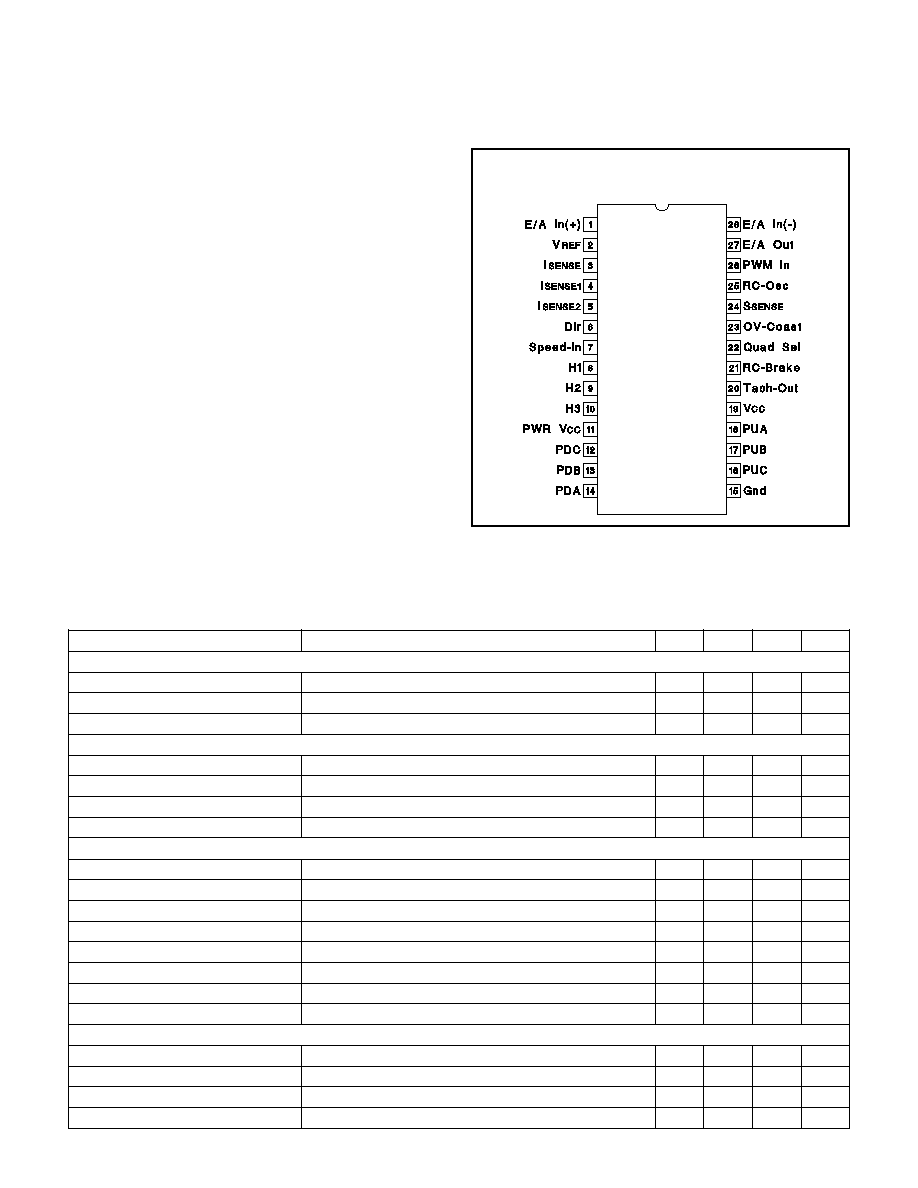
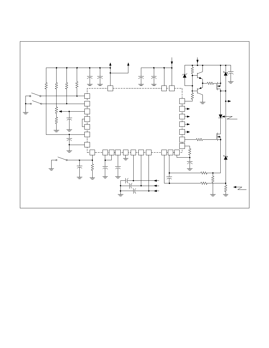
CONNECTION DIAGRAM
Note 3: This pinout applies to the SOIC (DW), PLCC (Q), and
LCC (L) packages (ie. pin 22 has the same function on all
packages.)
DIL-28 (TOP VIEW)
J or N PACKAGE

3
UC1625
UC2625
UC3625
ELECTRICAL CHARACTERISTICS: Unless otherwise stated, these specifications apply for: T
A
= 25
∞C; Pwr V
CC
= V
CC
= 12V;
R
OSC =
20k to V
REF
; C
OSC
= 2nF; R
TACH
= 33k; C
TACH
= 10nF; and all outputs unloaded. T
A
= T
J.
PARAMETER
TEST CONDITIONS
MIN
TYP
MAX
UNITS
PWM Amp/Comparator (cont.)
E/A Out Range
0.25
3.50
V
S
START
Pull-up Current
To 0V
≠16
≠10
≠5
µA
S
START
Discharge Current
To 2.5V
0.1
0.4
3.0
mA
S
START Restart Threshold
0.1
0.2
0.3
V
Current Amp
Gain
I
SENSE1
= .3V, I
SENSE2
= .5V to .7V
1.75
1.95
2.15
V/V
Level Shift
I
SENSE1
= .3V, I
SENSE2
= .3V
2.4
2.5
2.65
V
Peak Current Threshold
I
SENSE1
= 0V, Force I
SENSE2
0.14
0.20
0.26
V
Over Current Threshold
I
SENSE1
= 0V, Force I
SENSE2
0.26
0.30
0.36
V
I
SENSE1
, I
SENSE2
Input Current
To 0V
≠850
≠320
0
µA
I
SENSE1
, I
SENSE2
Offset Current
To 0V
±2
±12
µA
Range I
SENSE1
, I
SENSE2
≠1
2
V
Tachometer/Brake
Tach-Out High Level
Over Operating Range, 10k to 2.5V
4.7
5
5.3
V
Tach-Out Low Level
Over Operating Range, 10k to 2.5V
0.2
V
On Time
170
220
280
µs
On Time Change With Temp
Over Operating Range
0.1
%
RC-Brake Input Current
To 0V
≠4.0
≠1.9
mA
Threshold to Brake, RC-Brake
Over Operating Range
0.8
1.0
1.2
V
Brake Hysteresis, RC-Brake
0.09
V
Speed-In Threshold
Over Operating Range
220
257
290
mV
Speed-In Input Current
≠30
≠5
30
µA
Low-Side Drivers
Voh, ≠1mA, Down From V
CC
Over Operating Range
1.60
2.1
V Voh, ≠50mA, Down From V
CC
Over Operating Range
1.75
2.2
V
Vol, 1mA
Over Operating Range
0.05
0.4
V
Vol, 50mA
Over Operating Range
0.36
0.8
V
Rise/Fall Time
10% to 90% Slew Time, into 1nF
50
ns
High-Side Drivers
Vol, 1mA
Over Operating Range
0.1
0.4
V
Vol, 50mA
Over Operating Range
1.0
1.8
V
Leakage Current
Output Voltage = 50V
25
µA
Fall Time
10% to 90% Slew Time, 50mA Load
50
ns
Oscillator
Frequency
40
50
60
kHz
Frequency
Over Operating Range
35
65
kHz
Reference
Output Voltage
4.9
5.0
5.1
V
Output Voltage
Over Operating Range
4.7
5.0
5.3
V
Load Regulation
0mA to ≠20mA Load
≠40
≠5
mV
Line Regulation
10V to 18V V
CC
≠10
≠1
10
mV
Short Circuit Current
Over Operating Range
50
100
150
mA
4
UC1625
UC2625
UC3625
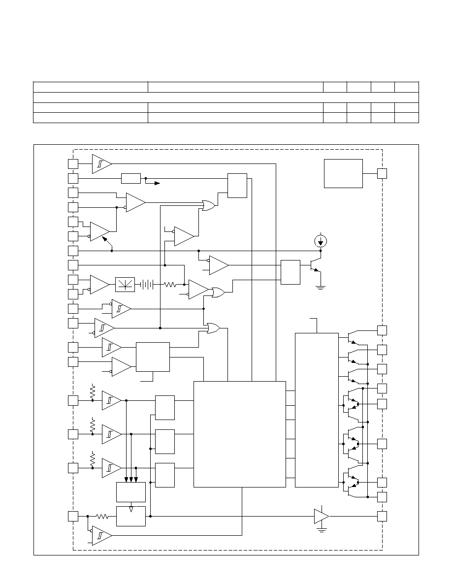
22
26
25
2
Quad Sel
RC-Osc
PWM In
27
28
1
E/A Out
E/A In(+)
E/A In (≠)
OSC
S
Q
R
S
Q
R
PWM CLOCK
24
SSTART
3
ISENSE
4
ISENSE1
5
ISENSE2
19
VCC
23
OV-Coast
6
Dir
7
Speed-In
2X
2.5V
250
2.9V
Q1
10
µA
3.1V
9V
DIRECTION
LATCH
0.25V
PWM CLOCK
8
H1
9
H2
L
Q
D
L
Q
D
L
Q
D
9
H3
+5V
+5V
+5V
EDGE
DETECT
ONE
SHOT
21
RC-Brake
2k
1V
DIR
COAST
CHOP
QUAD
H2
H1
H3
BRAKE
DECODER
CROSS
CONDUCTION
PROTECTION
LATCHES
18
PUA
17
PUB
16
PUC
14
PDA
13
PDB
12
PDC
15
GND
20
Tach-Out
11
Pwr Vcc
+5V
VREF
5V
REFERENCE
PWM
CLOCK
1.75V
ABS VALUE
0.2V
BLOCK DIAGRAM
ELECTRICAL CHARACTERISTICS: Unless otherwise stated, these specifications apply for: T
A
= 25
∞C; Pwr V
CC
= V
CC
= 12V;
R
OSC =
20k to V
REF
; C
OSC
= 2nF; R
TACH
= 33k; C
TACH
= 10nF; and all outputs unloaded. T
A
= T
J.
PARAMETER
TEST CONDITIONS
MIN
TYP
MAX
UNITS
Miscellaneous
Output Turn-On Delay
1
µs
Output Turn-Off Delay
1
µs
UDG-99044

5
UC1625
UC2625
UC3625
Dir, Speed-In: The position decoder logic translates the
Hall signals and the Dir signal to the correct driver sig-
nals (PUs and PDs). To prevent output stage damage,
the signal on Dir is first loaded into a direction latch,
then shifted through a two-bit register.
As long as Speed-In is less than 250mV, the direction
latch is transparent. When Speed-In is higher than
250mV, the direction latch inhibits all changes in direc-
tion. Speed-In can be connected to Tach-Out through a
filter, so that the direction latch is only transparent when
the motor is spinning slowly, and has too little stored en-
ergy to damage power devices.
Additional circuitry detects when the input and output of
the direction latch are different, or when the input and
output of the shift register are different, and inhibits all
output drives during that time. This can be used to allow
the motor to coast to a safe speed before reversing.
The shift register guarantees that direction can't be
changed instantaneously. The register is clocked by the
PWM oscillator, so the delay between direction changes
is always going to be between one and two oscillator pe-
riods. At 40kHz, this corresponds to a delay of between
25
µs and 50µs. Regardless of output stage, 25µs dead
time should be adequate to guarantee no overlap
cross-conduction. Toggling DIR will cause an output
pulse on Tach-Out regardless of motor speed.
E/A In(+), E/A In(≠), E/A Out, PWM In: E/A In(+) and
E/A In(≠) are not internally committed to allow for a wide
variety of uses. They can be connected to the I
SENSE
, to
Tach-Out through a filter, to an external command volt-
age, to a D/A converter for computer control, or to an-
other op amp for more elegant feedback loops. The
error amplifier is compensated for unity gain stability, so
E/A Out can be tied to E/A In(≠) for feedback and major
loop compensation.
E/A Out and PWM In drive the PWM comparator. For
voltage-mode PWM systems, PWM In can be connected
to RC-Osc. The PWM comparator clears the PWM latch,
commanding the outputs to chop.
The error amplifier can be biased off by connecting E/A
In(≠) to a higher voltage than E/A In(+). When biased
off, E/A Out will appear to the application as a resistor to
ground. E/A Out can then be driven by an external am-
plifier.
GND: All thresholds and outputs are referred to the
GND pin except for the PD and PU outputs.
H1, H2, H3: The three shaft-position sensor inputs con-
sist of hysteresis comparators with input pull-up resis-
tors. Logic thresholds meet TTL specifications and can
be driven by 5V CMOS, 12V CMOS, NMOS, or
open-collectors.
Connect these inputs to motor shaft position sensors
that are positioned 120 electrical degrees apart. If noisy
signals are expected, zener clamp and filter these inputs
with 6V zeners and an RC filter. Suggested filtering
components are 1k
and 2nF. Edge skew in the filter is
not a problem, because sensors normally generate
modified Gray code with only one output changing at a
time, but rise and fall times must be shorter than 20
µs
for correct tachometer operation.
Motors with 60 electrical degree position sensor coding
can be used if one or two of the position sensor signals
is inverted.
I
SENSE1
, I
SENSE2
, I
SENSE
: The current sense amplifier
has a fixed gain of approximately two. It also has a
built-in level shift of approximately 2.5V. The signal ap-
pearing on I
SENSE
is:
(
)
(
)
I
V
ABS I
I
SENSE
SENSE
SENSE
=
+
∑
2 5
2
1
2
.
≠
I
SENSE1
and I
SENSE2
are interchangeable and can be
used as differential inputs. The differential signal applied
can be as high as
±0.5V before saturation.
If spikes are expected on I
SENSE1
or I
SENSE2
, they are
best filtered by a capacitor from I
SENSE
to ground. Fil-
tering this way allows fast signal inversions to be cor-
rectly processed by the absolute value circuit. The
peak-current comparator allows the PWM to enter a cur-
rent-limit mode with current in the windings never ex-
ceeding approximately 0.2V/R
SENSE.
The over current
comparator provides a fail-safe shutdown in the unlikely
case of current exceeding 0.3V/R
SENSE.
Then, soft start
is commanded, and all outputs are turned off until the
high current condition is removed. It is often essential to
use some filter driving I
SENSE1
and I
SENSE2
to reject ex-
treme spikes and to control slew rate. Reasonable start-
ing values for filter components might be 250
series
resistors and a 5nF capacitor between I
SENSE1
and
I
SENSE2
. Input resistors should be kept small and
matched to maintain gain accuracy.
OV-Coast: This input can be used as an over-voltage
shutdown in put, as a coast input, or both. This input
can be driven by TTL, 5V CMOS, or 12V CMOS.
PIN DESCRIPTIONS

6
UC1625
UC2625
UC3625
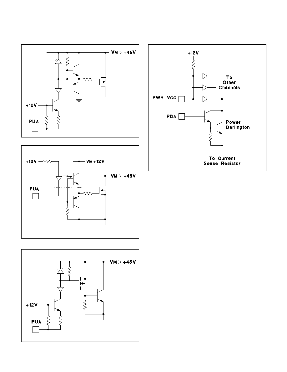
PDA, PDB, PDC: These outputs can drive the gates of
N-Channel power MOSFETs directly or they can drive
the bases of power Darlingtons if some form of current
limiting is used. They are meant to drive low-side power
devices in high-current output stages. Current available
from these pins can peak as high as 0.5A. These out-
puts feature a true totem-pole output stage. Beware of
exceeding IC power dissipation limits when using these
outputs for high continuous currents. These outputs pull
high to turn a "low-side" device on (active high).
PUA, PUB, PUC: These outputs are open-collector,
high-voltage drivers that are meant to drive high-side
power devices in high-current output stages. These are
active low outputs, meaning that these outputs pull low
to command a high-side device on. These outputs can
drive low-voltage PNP Darlingtons and P-channel
MOSFETs directly, and can drive any high-voltage de-
vice using external charge-pump techniques, trans-
former signal coupling, cascode level-shift transistors, or
opto-isolated drive (high-speed opto devices are recom-
mended). (See applications).
PWR V
CC
: This supply pin carries the current sourced
by the PD outputs. When connecting PD outputs directly
to the bases of power Darlingtons, the PWR V
CC
pin can
be current limited with a resistor. Darlington outputs can
also be "Baker Clamped" with diodes from collectors
back to PWR V
CC
. (See Applications)
Quad Sel: The IC can chop power devices in either of
two modes, referred to as "two-quadrant" (Quad Sel low)
and
"four-quadrant"
(Quad
Sel
high).
When
two-quadrant chopping, the pull-down power devices
are chopped by the output of the PWM latch while the
pull-up drivers remain on. The load will chop into one
commutation diode, and except for back-EMF, will ex-
hibit slow discharge current and faster charge current.
Two-quadrant chopping can be more efficient than
four-quadrant.
When four-quadrant chopping, all power drivers are
chopped by the PWM latch, causing the load current to
flow into two diodes during chopping. This mode exhibits
better control of load current when current is low, and is
preferred in servo systems for equal control over accel-
eration and deceleration. The Quad Sel input has no ef-
fect on operation during braking.
RC-Brake: Each time the Tach-Out pulses, the capaci-
tor tied to RC-Brake discharges from approximately
3.33V down to 1.67V through a resistor. The tachometer
pulse width is approximately T = 0.67 R
T
C
T
, where R
T
and C
T
are a resistor and capacitor from RC-Brake to
ground. Recommended values for R
T
are 10k
to
500k
, and recommended values for C
T
are 1nF to
100nF, allowing times between 5
µs and 10ms. Best ac-
curacy and stability are achieved with values in the cen-
ters of those ranges.
RC-Brake also has another function. If RC-Brake pin is
pulled below the brake threshold, the IC will enter brake
mode. This mode consists of turning off all three
high-side devices, enabling all three low-side devices,
and disabling the tachometer. The only things that in-
hibit
low-side
device
operation
in
braking
are
low-supply, exceeding peak current, OV-Coast com-
mand, and the PWM comparator signal. The last of
these means that if current sense is implemented such
that the signal in the current sense amplifier is propor-
tional to braking current, the low-side devices will brake
the motor with current control. (See applications) Sim-
pler current sense connections will result in uncontrolled
braking and potential damage to the power devices.
RC-Osc: The UC3625 can regulate motor current using
fixed-frequency pulse width modulation (PWM). The
RC-Osc pin sets oscillator frequency by means of timing
resistor R
OSC
from the RC-Osc pin to V
REF
and capaci-
tor C
OSC
from RC-Osc to Gnd. Resistors 10k
to
100k
and capacitors 1nF to 100nF will work best, but
frequency should always be below 500kHz. Oscillator
frequency is approximately:
(
)
F
R
C
OSC
OSC
=
∑
2
Additional components can be added to this device to
cause it to operate as a fixed off-time PWM rather than
a fixed frequency PWM, using the RC-Osc pin to select
the monostable time constant.
The voltage on the RC-Osc pin is normally a ramp of
about 1.2V peak-to-peak, centered at approximately
1.6V. This ramp can be used for voltage-mode PWM
control, or can be used for slope compensation in cur-
rent-mode control.
S
START
: Any time that V
CC
drops below threshold or the
sensed current exceeds the over-current threshold, the
soft-start latch is set. When set, it turns on a transistor
that pulls down on S
START.
Normally, a capacitor is con-
nected to this pin, and the transistor will completely dis-
charge the capacitor. A comparator senses when the
NPN transistor has completely discharged the capacitor,
and allows the soft-start latch to clear when the fault is
removed. When the fault is removed, the soft-start ca-
pacitor will charge from the on-chip current source.
PIN DESCRIPTIONS (cont.)
7
UC1625
UC2625
UC3625
S
START
clamps the output of the error amplifier, not al-
lowing the error amplifier output voltage to exceed
S
START
regardless of input. The ramp on RC-Osc can
be applied to PWM In and compared to E/A Out. With
S
START
discharged below 0.2V and the ramp minimum
being approximately 1.0V, the PWM comparator will
keep the PWM latch cleared and the outputs off. As
S
START
rises, the PWM comparator will begin to
duty-cycle modulate the PWM latch until the error ampli-
fier inputs overcome the clamp. This provides for a safe
and orderly motor start-up from an off or fault condition.
Tach-Out: Any change in the H1, H2, or H3 inputs loads
data from these inputs into the position sensor latches.
At the same time data is loaded, a fixed-width 5V pulse
is triggered on Tach-Out. The average value of the volt-
age on Tach-Out is directly proportional to speed, so
this output can be used as a true tachometer for speed
feedback with an external filter or averaging circuit
which usually consists of a resistor and capacitor.
Whenever Tach-Out is high, the position latches are in-
hibited, such that during the noisiest part of the commu-
tation cycle, additional commutations are not possible.
Although this will effectively set a maximum rotational
speed, the maximum speed can be set above the high-
est expected speed, preventing false commutation and
chatter.
V
CC
: This device operates with supplies between 10V
and 18V. Under-voltage lockout keeps all outputs off be-
low 7.5V, insuring that the output transistors never turn
on until full drive capability is available. Bypass V
CC
to
ground with an 0.1
µF ceramic capacitor. Using a 10µF
electrolytic bypass capacitor as well can be beneficial in
applications with high supply impedance.
V
REF
: This pin provides regulated 5 volts for driving
Hall-effect devices and speed control circuitry. V
REF
will
reach +5V before V
CC
enables, ensuring that Hall-effect
devices powered from V
REF
will become active before
the UC3625 drives any output. Although V
REF
is current
limited, operation over 30mA is not advised. For proper
performance V
REF
should be bypassed with at least a
0.1
µF capacitor to ground.
PIN DESCRIPTIONS (cont.)
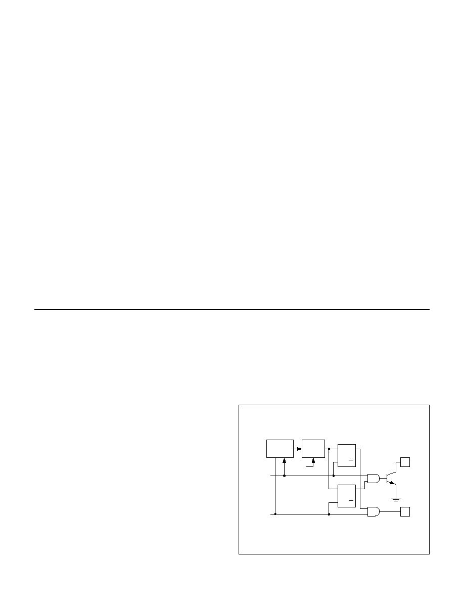
Cross Conduction Prevention
The UC3625 inserts delays to prevent cross conduction
due to overlapping drive signals. However, some thought
must always be given to cross conduction in output stage
design because no amount of dead time can prevent fast
slewing signals from coupling drive to a power device
through a parasitic capacitance.
The UC3625 contains input latches that serve as noise
blanking
filters.
These
latches
remain
transparent
through any phase of a motor rotation and latch immedi-
ately after an input transition is detected. They remain
latched for two cycles of the PWM oscillator. At a PWM
oscillator speed of 20kHz, this corresponds to 50
µs to
100
µs of blank time which limits maximum rotational
speed to 100kRPM for a motor with six transitions per ro-
tation or 50kRPM for a motor with 12 transitions per rota-
tion.
This prevents noise generated in the first 50
µs of a tran-
sition from propagating to the output transistors and
causing cross≠conduction or chatter.
The UC3625 also contains six flip flops corresponding to
the six output drive signals. One of these flip flops is set
every time that an output drive signal is turned on, and
cleared two PWM oscillator cycles after that drive signal
is turned off. The output of each flip flop is used to inhibit
drive to the opposing output (see below). In this way, it is
impossible to turn on driver PUA and PDA at the same
time. It is also impossible for one of these drivers to turn
on without the other driver having been off for at least
two PWM oscillator clocks.
APPLICATION INFORMATION
EDGE
FINDER
SHIFT
REG
S
Q
Q
R
S
Q
Q
R
PUA
PDA
PULL
DOWN
PULL UP
FROM
DECODER
PWM
CLK
Figure 1. Cross conduction prevention.

8
UC1625
UC2625
UC3625
0.001
0.01
0.1
100Hz
1kHz
10kHz
100kHz
1MHz
Rosc
- 30k
Rosc
- 10k
Rosc
- 100k
Oscillator
Frequency
C
( F)
OSC
µ
C
( F)
OSC
µ
TYPICAL CHARACTERISTICS
Figure 2. Oscillator frequency vs. C
OSC
and R
OSC
.
0.001
0.01
0.1
1 s
µ
1 0 s
µ
100 s
µ
1ms
10ms
100ms
R -
500k
T
R -
500k
T
R -
100k
T
R -
100k
T
R -
30k
T
R -
30k
T
R -
10k
T
R -
10k
T
On
T
ime
C ( F)
T
µ
Figure 3. Tachometer on time vs R
T
and C
T
.
Figure 4. Supply current vs. temperature.
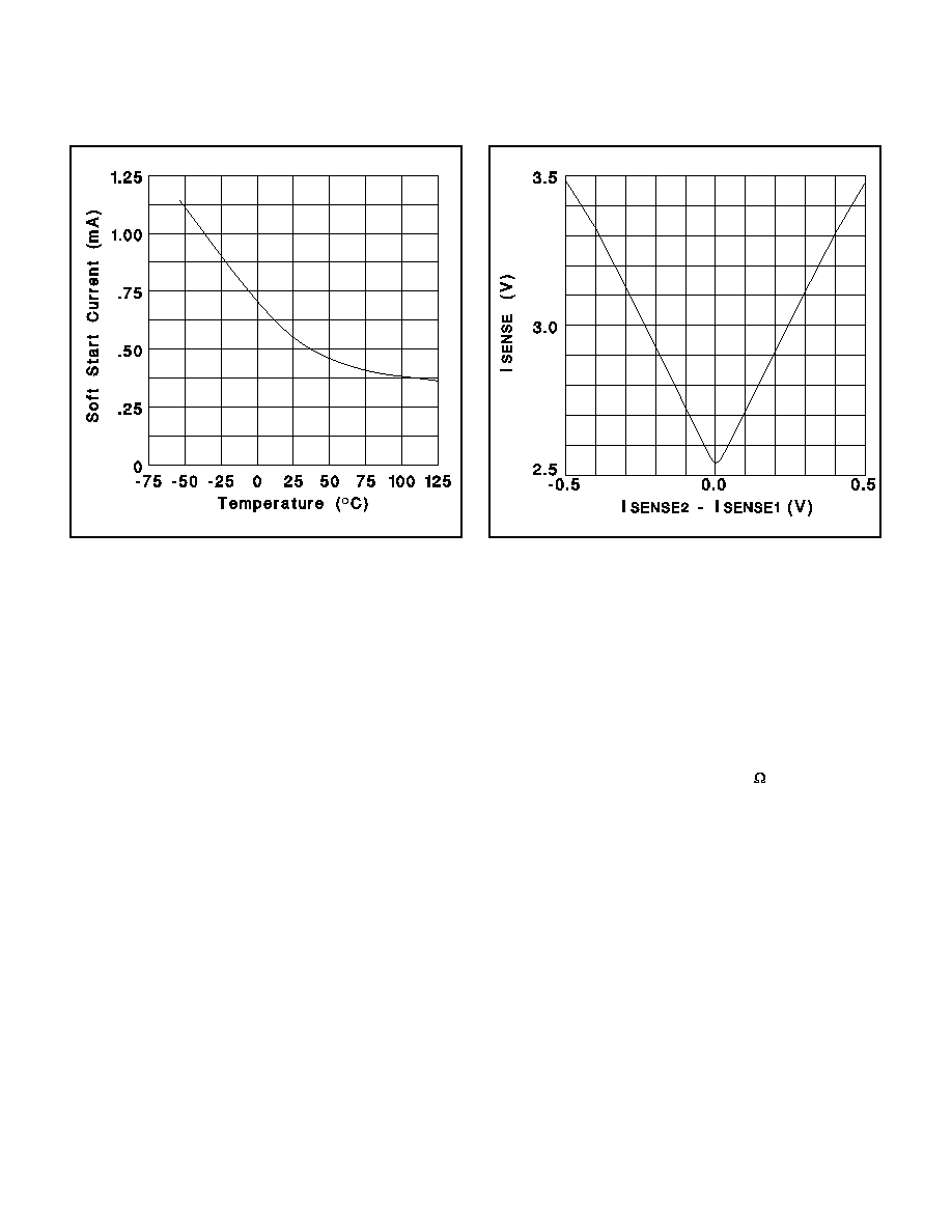
Figure 5. Soft start pull-up current vs temperature.
9
UC1625
UC2625
UC3625
Figure 6. Soft start discharge current vs.
temperature.
TYPICAL CHARACTERISTICS (cont.)
Figure 7. Current sense amplifier transfer function.
Power Stage Design
The UC3625 is useful in a wide variety of applications,
including high-power in robotics and machinery.
The
power output stages used in such equipment can take a
number of forms, according to the intended perfor-
mance and purpose of the system. Below are four differ-
ent
power
stages
with
the
advantages
and
disadvantages of each shown.
For high-frequency chopping, fast recovery circulating
diodes are essential. Six are required to clamp the wind-
ings. These diodes should have a continuous current
rating at least equal to the operating motor current,
since diode conduction duty-cycle can be high.
For
low-voltage systems, Schottky diodes are preferred. In
higher voltage systems, diodes such as Microsemi
UHVP high voltage platinum rectifiers are recom-
mended.
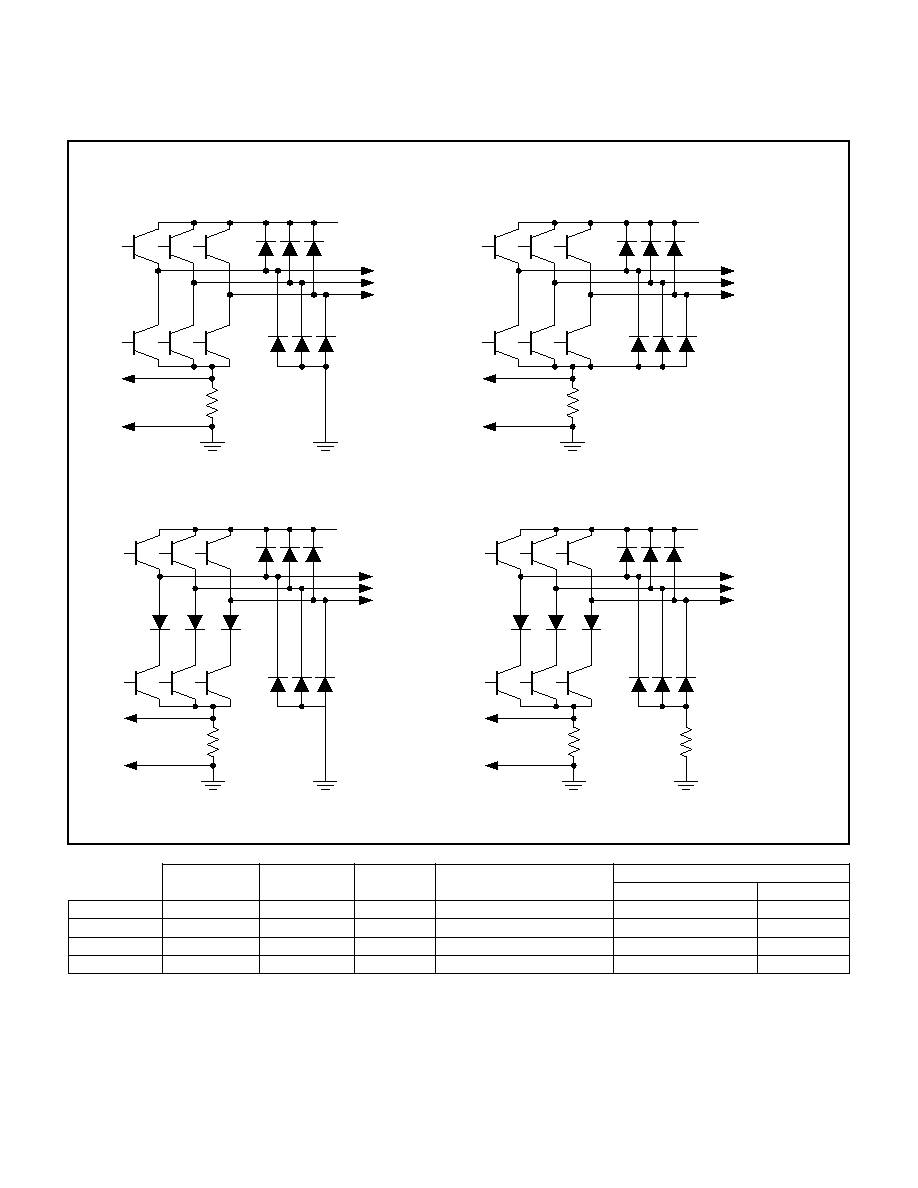
In a pulse-by-pulse current control arrangement, current
sensing is done by resistor R
S
, through which the tran-
sistor's currents are passed (Fig. A, B, and C). In these
cases, R
D
is not needed. The low-side circulating di-
odes go to ground and the current sense terminals of
the UC3625 (I
SENSE1
and I
SENSE2
) are connected to R
S
through a differential RC filter. The input bias current of
the current sense amplifier will cause a common mode
offset voltage to appear at both inputs, so for best accu-
racy, keep the filter resistors below 2k
and matched.
The current that flows through R
S
is discontinuous be-
cause of chopping. It flows during the on time of the
power stage and is zero during the off time. Conse-
quently, the voltage across R
S
consists of a series of
pulses, occurring at the PWM frequency, with a peak
value indicative of the peak motor current.
To sense average motor current instead of peak cur-
rent, add another current sense resistor (R
D
in Fig. D) to
measure current in the low-side circulating diodes, and
operate in four quadrant mode (pin 22 high). The nega-
tive voltage across R
D
is corrected by the absolute
value current sense amplifier. Within the limitations im-
posed by Table 1, the circuit of Fig. B can also sense
average current.
APPLICATION INFORMATION (cont.)
10
UC1625
UC2625
UC3625
TO
MOTOR
R
S
FIGURE B
TO
MOTOR
R
S
FIGURE A
TO
MOTOR
R
S
FIGURE C
TO
MOTOR
R
S
R
D
FIGURE D
2
4
SAFE
POWER
CURRENT SENSE
QUADRANT
QUADRANT
BRAKING
REVERSE
PULSE BY PULSE
AVERAGE
FIGURE A
YES
NO
NO
NO
YES
NO
FIGURE B
YES
YES
NO
IN 4-QUAD MODE ONLY
YES
YES
FIGURE C
YES
YES
YES
IN -4QUAD MODE ONLY
YES
NO
FIGURE D
YES
YES
YES
IN-4QUADMODE ONLY
YES
YES
APPLICATION INFORMATION (cont.)
11
UC1625
UC2625
UC3625
For drives where speed is critical, P-Channel MOSFETs
can be driven by emitter followers as shown in Fig. 8.
Here, both the level shift NPN and the PNP must with-
stand high voltages. A zener diode is used to limit
gate-source voltage on the MOSFET. A series gate re-
sistor is not necessary, but always advisable to control
overshoot and ringing.
High-voltage optocouplers can quickly drive high-voltage
MOSFETs if a boost supply of at least 10 volts greater
than the motor supply is provided (See Fig. 9.) To protect
the MOSFET, the boost supply should not be higher than
18 volts above the motor supply.
For under 200V 2-quadrent applications, a power NPN
driven by a small P-Channel MOSFET will perform well
as a high-side driver as in Fig. 10. A high voltage
small-signal NPN is used as a level shift and a high volt-
age low-current MOSFET provides drive. Although the
NPN will not saturate if used within its limitations, the
base-emitter resistor on the NPN is still the speed limiting
component.
Fig. 11 shows a power NPN Darlington drive technique
using a clamp to prevent deep saturation. By limiting sat-
uration of the power device, excessive base drive is mini-
mized and turn-off time is kept fairly short. Lack of base
series resistance also adds to the speed of this ap-
proach.
Figure 9. Optocoupled N-channel high-side driver.
Figure 8. Fast high-side P-channel driver.
APPLICATION INFORMATION (cont.)
Figure 11. Power NPN low-side driver.
Figure 10. Power NPN high-side driver.

12
UC1625
UC2625
UC3625
Fast High-Side N-Channel Driver with Transformer
Isolation
A small pulse transformer can provide excellent isolation
between the UC3625 and a high-voltage N-Channel
MOSFET while also coupling gate drive power. In this
circuit (shown in Fig. 12), a UC3724 is used as a trans-
former driver/encoder that duty-cycle modulates the
transformer with a 150kHz pulse train. The UC3725 recti-
fies this pulse train for gate drive power, demodulates the
signal, and drives the gate with over 2 amp peak current.
Both the UC3724 and the UC3725 can operate up to
500kHz if the pulse transformer is selected appropriately.
To raise the operating frequency, either lower the timing
resistor of the UC3724 (1k
min), lower the timing ca-
pacitor of the UC3724 (500pF min) or both.
If there is significant capacitance between transformer
primary and secondary, together with very high output
slew rate, then it may be necessary to add clamp diodes
from the transformer primary to +12V and ground. Gen-
eral purpose small signal switching diodes such as
1N4148 are normally adequate.
The UC3725 also has provisions for MOSFET current
limiting. Consult the UC3725 data sheet for more infor-
mation on implementing this.
Computational Truth Table
This table shows the outputs of the gate drive and open
collector outputs for given hall input codes and direction
signals. Numbers at the top of the columns are pin
numbers.
These ICs operate with position sensor encoding that
has either one or two signals high at a time, never all low
or all high. This coding is sometimes referred to as "120
∞
Coding" because the coding is the same as coding with
position sensors spaced 120 magnetic degrees about
the rotor. In response to these position sense signals,
only one low-side driver will turn on (go high) and one
high-side driver will turn on (pull low) at any time.
2
8
7
1
6
5
4
3
1
2
6
7
4
8
UC3724N
UC3725N
1:2
PUA
33k
3
+12V
1nF
5k
100nF
VMOTOR
TO MOTOR
APPLICATION INFORMATION (cont.)
Figure 12. Fast high-side N-channel driver with transformer isolation.
INPUTS
OUTPUTS
DIR
H1
H2
H3
Low-Side
High-Side
6
8
9
10
12
13
14
16
17
18
1
0
0
1
L
H
L
L
H
H
1
0
1
1
L
L
H
L
H
H
1
0
1
0
L
L
H
H
L
H
1
1
1
0
H
L
L
H
L
H
1
1
0
0
H
L
L
H
H
L
1
1
0
1
L
H
L
H
H
L
0
1
0
1
L
L
H
H
L
H
0
1
0
0
L
L
H
L
H
H
0
1
1
0
L
H
L
L
H
H
0
0
1
0
L
H
L
H
H
L
0
0
1
1
H
L
L
H
H
L
0
0
0
1
H
L
L
H
L
H
X
1
1
1
L
L
L
H
H
H
X
0
0
0
L
L
L
H
H
H
Table I. Computational truth table.
UDG-99047
13
UC1625
UC2625
UC3625
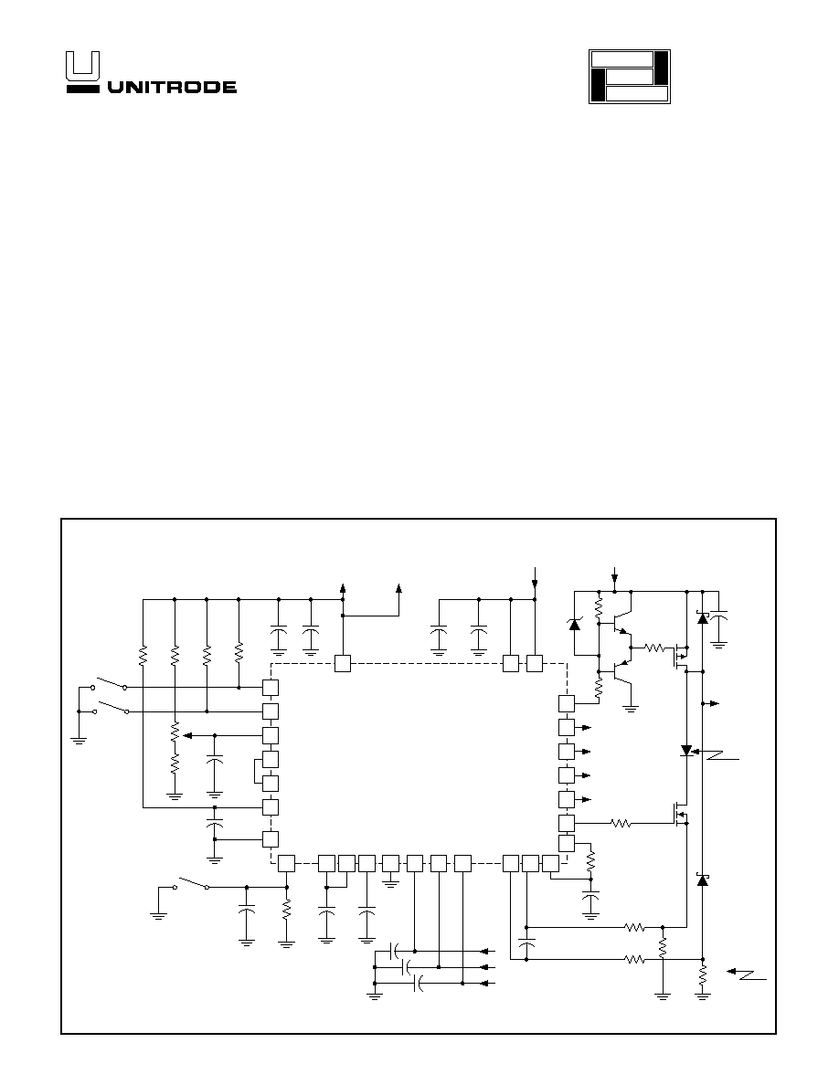
21
27
25
22
6
28
1
15
24
3
26
10k
3k
10k
2
19
20
16
11
20
µF
100nF
20
µF
100nF
+
R
OSC
33k
2200pF
C
OSC
68k
R
T
3nF
C
T
BRAKE
5nF
100nF
23
8
9
10
4
5
7
2nF
2nF
2nF
100nF
10k
5nF
240
240
17
18
14
13
12
3k
2N3906
100nF
1k
4k
TO OTHER
CHANNELS
TO OTHER
CHANNELS
10
2N3904
10
IRF9350
IRF532
3k
FROM
HALL
SENSORS
VMOTOR
+15V
+5V TO HALL
SENSORS
VREF
0.02
R
S
TO
MOTOR
0.02
R
D
REQUIRED
FOR
AVERAGE
CURRENT
SENSING
REQUIRED
FOR BRAKE
AND FAST
REVERSE
100
µF
+
UC3625
DIR
QUAD
APPLICATION INFORMATION (cont.)
Figure 13. 45V/8A brushless DC motor drive circuit.
N≠Channel power MOSFETs are used for low≠side driv-
ers, while P≠Channel power MOSFETs are shown for
high≠side drivers. Resistors are used to level shift the
UC3625 open≠collector outputs, driving emitter follow-
ers into the MOSFET gate. A 12V zener clamp insures
that the MOSFET gate≠source voltage will never exceed
12V. Series 10
gate resistors tame gate reactance,
preventing oscillations and minimizing ringing.
The oscillator timing capacitor should be placed close to
pins 15 and 25, to keep ground current out of the capac-
itor. Ground current in the timing capacitor causes oscil-
lator distortion and slaving to the commutation signal.
The potentiometer connected to pin 1 controls PWM
duty cycle directly, implementing a crude form of speed
control. This control is often referred to as "voltage
mode" because the potentiometer position sets the aver-
age motor voltage. This controls speed because
steady≠state motor speed is closely related to applied
voltage.
Pin 20 (Tach-Out) is connected to pin 7 (SPEED IN)
through an RC filter, preventing direction reversal while
the motor is spinning quickly. In two≠quadrant opera-
tion, this reversal can cause kinetic energy from the mo-
tor to be forced into the power MOSFETs.
A diode in series with the low-side MOSFETs facilitates
PWM current control during braking by insuring that
braking current will not flow backwards through low≠side
MOSFETs. Dual current≠sense resistors give continu-
ous current sense, whether braking or running in
four≠quadrant operation, an unnecessary luxury for
two≠quadrant operation.
The 68k
and 3nF tachometer components set maxi-
mum commutation time at 140
µs. This permits smooth
operation up to 35,000 RPM for four≠pole motors, yet
gives 140
µs of noise blanking after commutation.
UNITRODE CORPORATION
7 CONTINENTAL BLVD. ∑ MERRIMACK, NH 03054
TEL. (603) 424-2410 ∑ FAX (603) 424-3460
UDG-99045

PACKAGING INFORMATION
Orderable Device
Status
(1)
Package
Type
Package
Drawing
Pins Package
Qty
Eco Plan
(2)
Lead/Ball Finish
MSL Peak Temp
(3)
5962-9168901MXA
OBSOLETE
CDIP
J
28
TBD
Call TI
Call TI
UC1625J
OBSOLETE
CDIP
J
28
TBD
Call TI
Call TI
UC1625J883B
OBSOLETE
CDIP
J
28
TBD
Call TI
Call TI
UC1625L
OBSOLETE
LCCC
FK
28
TBD
Call TI
Call TI
UC1625L883B
OBSOLETE
LCCC
FK
28
TBD
Call TI
Call TI
UC2625DW
ACTIVE
SOIC
DW
28
20
Green (RoHS &
no Sb/Br)
CU NIPDAU
Level-2-260C-1 YEAR
UC2625DWTR
ACTIVE
SOIC
DW
28
1000 Green (RoHS &
no Sb/Br)
CU NIPDAU
Level-2-260C-1 YEAR
UC2625N
ACTIVE
PDIP
N
28
13
TBD
Call TI
Level-NA-NA-NA
UC2625Q
ACTIVE
PLCC
FN
28
37
TBD
Call TI
Level-2-220C-1 YEAR
UC2625QTR
ACTIVE
PLCC
FN
28
750
TBD
Call TI
Level-2-220C-1 YEAR
UC3625DW
ACTIVE
SOIC
DW
28
20
Green (RoHS &
no Sb/Br)
CU NIPDAU
Level-2-260C-1 YEAR
UC3625DWTR
ACTIVE
SOIC
DW
28
1000 Green (RoHS &
no Sb/Br)
CU NIPDAU
Level-2-260C-1 YEAR
UC3625N
ACTIVE
PDIP
N
28
13
TBD
Call TI
Level-NA-NA-NA
UC3625Q
ACTIVE
PLCC
FN
28
37
TBD
Call TI
Level-2-220C-1 YEAR
UC3625QTR
ACTIVE
PLCC
FN
28
750
TBD
Call TI
Level-2-220C-1 YEAR
(1)
The marketing status values are defined as follows:
ACTIVE: Product device recommended for new designs.
LIFEBUY: TI has announced that the device will be discontinued, and a lifetime-buy period is in effect.
NRND: Not recommended for new designs. Device is in production to support existing customers, but TI does not recommend using this part in
a new design.
PREVIEW: Device has been announced but is not in production. Samples may or may not be available.
OBSOLETE: TI has discontinued the production of the device.
(2)
Eco
Plan
-
The
planned
eco-friendly
classification:
Pb-Free
(RoHS)
or
Green
(RoHS
&
no
Sb/Br)
-
please
check
http://www.ti.com/productcontent
for the latest availability information and additional product content details.
TBD: The Pb-Free/Green conversion plan has not been defined.
Pb-Free (RoHS): TI's terms "Lead-Free" or "Pb-Free" mean semiconductor products that are compatible with the current RoHS requirements
for all 6 substances, including the requirement that lead not exceed 0.1% by weight in homogeneous materials. Where designed to be soldered
at high temperatures, TI Pb-Free products are suitable for use in specified lead-free processes.
Green (RoHS & no Sb/Br): TI defines "Green" to mean Pb-Free (RoHS compatible), and free of Bromine (Br) and Antimony (Sb) based flame
retardants (Br or Sb do not exceed 0.1% by weight in homogeneous material)
(3)
MSL, Peak Temp. -- The Moisture Sensitivity Level rating according to the JEDEC industry standard classifications, and peak solder
temperature.
Important Information and Disclaimer:The information provided on this page represents TI's knowledge and belief as of the date that it is
provided. TI bases its knowledge and belief on information provided by third parties, and makes no representation or warranty as to the
accuracy of such information. Efforts are underway to better integrate information from third parties. TI has taken and continues to take
reasonable steps to provide representative and accurate information but may not have conducted destructive testing or chemical analysis on
incoming materials and chemicals. TI and TI suppliers consider certain information to be proprietary, and thus CAS numbers and other limited
information may not be available for release.
In no event shall TI's liability arising out of such information exceed the total purchase price of the TI part(s) at issue in this document sold by TI
to Customer on an annual basis.
PACKAGE OPTION ADDENDUM
www.ti.com
19-Jul-2005
Addendum-Page 1

IMPORTANT NOTICE
Texas Instruments Incorporated and its subsidiaries (TI) reserve the right to make corrections, modifications,
enhancements, improvements, and other changes to its products and services at any time and to discontinue
any product or service without notice. Customers should obtain the latest relevant information before placing
orders and should verify that such information is current and complete. All products are sold subject to TI's terms
and conditions of sale supplied at the time of order acknowledgment.
TI warrants performance of its hardware products to the specifications applicable at the time of sale in
accordance with TI's standard warranty. Testing and other quality control techniques are used to the extent TI
deems necessary to support this warranty. Except where mandated by government requirements, testing of all
parameters of each product is not necessarily performed.
TI assumes no liability for applications assistance or customer product design. Customers are responsible for
their products and applications using TI components. To minimize the risks associated with customer products
and applications, customers should provide adequate design and operating safeguards.
TI does not warrant or represent that any license, either express or implied, is granted under any TI patent right,
copyright, mask work right, or other TI intellectual property right relating to any combination, machine, or process
in which TI products or services are used. Information published by TI regarding third-party products or services
does not constitute a license from TI to use such products or services or a warranty or endorsement thereof.
Use of such information may require a license from a third party under the patents or other intellectual property
of the third party, or a license from TI under the patents or other intellectual property of TI.
Reproduction of information in TI data books or data sheets is permissible only if reproduction is without
alteration and is accompanied by all associated warranties, conditions, limitations, and notices. Reproduction
of this information with alteration is an unfair and deceptive business practice. TI is not responsible or liable for
such altered documentation.
Resale of TI products or services with statements different from or beyond the parameters stated by TI for that
product or service voids all express and any implied warranties for the associated TI product or service and
is an unfair and deceptive business practice. TI is not responsible or liable for any such statements.
Following are URLs where you can obtain information on other Texas Instruments products and application
solutions:
Products
Applications
Amplifiers
amplifier.ti.com
Audio
www.ti.com/audio
Data Converters
dataconverter.ti.com
Automotive
www.ti.com/automotive
DSP
dsp.ti.com
Broadband
www.ti.com/broadband
Interface
interface.ti.com
Digital Control
www.ti.com/digitalcontrol
Logic
logic.ti.com
Military
www.ti.com/military
Power Mgmt
power.ti.com
Optical Networking
www.ti.com/opticalnetwork
Microcontrollers
microcontroller.ti.com
Security
www.ti.com/security
Telephony
www.ti.com/telephony
Video & Imaging
www.ti.com/video
Wireless
www.ti.com/wireless
Mailing Address:
Texas Instruments
Post Office Box 655303 Dallas, Texas 75265
Copyright
2005, Texas Instruments Incorporated