 | –≠–ª–µ–∫—Ç—Ä–æ–Ω–Ω—ã–π –∫–æ–º–ø–æ–Ω–µ–Ω—Ç: UC2705J | –°–∫–∞—á–∞—Ç—å:  PDF PDF  ZIP ZIP |

UC1705
UC2705
UC3705
TRUTH TABLE
INV
N.I
OUT
H
L
H
L
H
H
L
L
L
H
L
L
OUT = INV and N.I.
OUT = INV or N.I.
High Speed Power Driver
FEATURES
∑
1.5A Source/Sink Drive
∑
100 nsec Delay
∑
40 nsec Rise and Fall into
1000pF
∑
Inverting and Non-Inverting
Inputs
∑
Low Cross-Conduction Current
Spike
∑
Low Quiescent Current
∑
5V to 40V Operation
∑
Thermal Shutdown Protection
∑
MINIDIP and Power Packages
CONNECTION DIAGRAMS
BLOCK DIAGRAM
DESCRIPTION
The UC1705 family of power drivers is made with a high speed Schottky pro-
cess to interface between low-level control functions and high-power switching
devices - particularly power MOSFETs. These devices are also an optimum
choice for capacitive line drivers where up to 1.5 amps may be switched in ei-
ther direction. With both Inverting and Non-Inverting inputs available, logic sig-
nals of either polarity may be accepted, or one input can be used to gate or
strobe the other.
Supply voltages for both V
S
and V
C
can independently range from 5V to 40V.
For additional application details, see the UC1707/3707 data sheet.
The UC1705 is packaged in an 8-pin hermetically sealed CERDIP for -55∞C to
+125∞C operation. The UC3705 is specified for a temperature range of 0∞C to
+70∞C and is available in either a plastic minidip or a 5-pin, power TO-220
package.
application
INFO
available
DIL-8 MINIDIP, SOIC-8
(TOP VIEW)
N or J Package, D Package
5-PIN TO-220
(TOP VIEW)
T Package
JANUARY 1994 - REVISED AUGUST 2000 - SLUS370A
2
ABSOLUTE MAXIMUM RATINGS
N-Pkg
J-Pkg
T-Pkg
Supply Voltage, V
IN
. . . . . . . . . . . . . . . . . . . . . . . . . . . . . . . . 40V . . . . . . . . . . . . . . . . . . . 40V . . . . . . . . . . . . . . . . . . . 40V
Collector Supply Voltage, V
C
. . . . . . . . . . . . . . . . . . . . . . . . . 40V . . . . . . . . . . . . . . . . . . . 40V . . . . . . . . . . . . . . . . . . . 40V
Output Current (Source or Sink)
Steady-State. . . . . . . . . . . . . . . . . . . . . . . . . . . . . . . . . .
±
500mA. . . . . . . . . . . . . . . .
±
500mA. . . . . . . . . . . . . . . . .
±
1.0A
Peak Transient . . . . . . . . . . . . . . . . . . . . . . . . . . . . . . . . .
±
1.5A. . . . . . . . . . . . . . . . . .
±
1.0A. . . . . . . . . . . . . . . . . .
±
2.0A
Capacitive Discharge Energy . . . . . . . . . . . . . . . . . . . . . . 20
µ
J
. . . . . . . . . . . . . . . . . . . . 15
µ
J
. . . . . . . . . . . . . . . . . . . . 50
µ
J
Digital Inputs (See Note) . . . . . . . . . . . . . . . . . . . . . . . . . . . . 5.5V. . . . . . . . . . . . . . . . . . . 5.5V. . . . . . . . . . . . . . . . . . . 5.5V
Power Dissipation at T
A
= 25∞C (See Note) . . . . . . . . . . . . . . 1W. . . . . . . . . . . . . . . . . . . . 1W. . . . . . . . . . . . . . . . . . . . 3W
Power Dissipation at T
A
(Leads/Case) = 25∞C (See Note) . . . 3W. . . . . . . . . . . . . . . . . . . . 2W . . . . . . . . . . . . . . . . . . . 25W
Operating Temperature Range . . . . . . . . . . . . . . . . . . . . 0∞C to +70∞C . . . . . . . . . . -55∞C to +125∞C . . . . . . . . . . 0∞C to +70∞C
Storage Temperature Range . . . . . . . . . . . . . . . . . . . . -65∞C to +150∞C . . . . . . . . . -65∞C to +150∞C . . . . . . . . . -65∞C to +150∞C
Lead Temperature (Soldering, 10 seconds) . . . . . . . . . . . . . 300∞C . . . . . . . . . . . . . . . . . 300∞C . . . . . . . . . . . . . . . . . 300∞C
Note: All currents are positive into, negative out of the specified terminal.
Digital Drive can exceed 5.5V if input current is limited to 10mA
Consult Packaging Section of Databook for thermal limitations and considerations of package.
UC1705
UC2705
UC3705
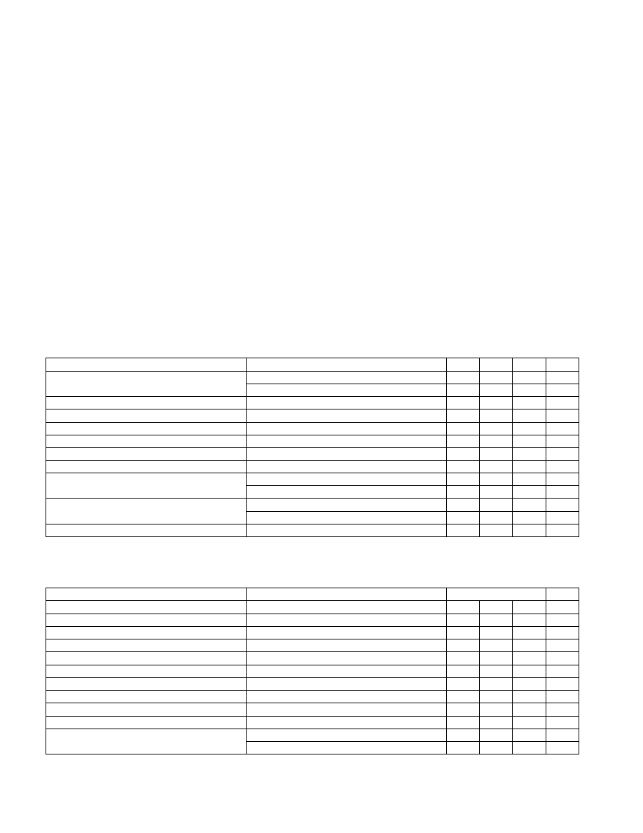
TYPICAL SWITCHING CHARACTERISTICS:
PARAMETERS
TEST CONDITIONS
OUTPUT C
L
=
UNIT
From Inv. Input to Output:
open
1.0
2.2
nF
Rise Time Delay
60
60
60
ns
10% to 90% Rise
20
40
60
ns
Fall Time Delay
60
60
60
ns
90% to 10% Fall
25
40
50
ns
From N. I. Input to Output:
Rise Time Delay
90
90
90
ns
10% to 90% Rise
20
40
60
ns
Fall Time Delay
60
60
60
ns
90% to 10% Fall
25
40
50
ns
V
C
Cross-Conduction
Current Spike Duration
Ouput Rise
25
ns
Output Fall
0
ns
PARAMETERS
TEST CONDITIONS
MIN
TYP
MAX
UNITS
V
S
Supply Current
V
S
= 40V, (Outputs High, T Pkg)
6
8
mA
V
S
= 40V, (Outputs Low, T Pkg)
8
12
mA
V
C
Supply Current (N, J Only)
V
C
= 40V, Outputs Low
2
4
mA
V
C
Leakage Current (N, J Only)
V
S
= 0, V
C
= 30V
0.05
0.1
mA
Digital Input Low Level
0.8
V
Digital Input High Level
2.2
V
Input Current
V
I
= 0
-0.6
-1.0
mA
Input Leakage
V
I
= 5V
0.05
0.1
mA
Output High Sat., V
C
-V
O
I
O
= -50mA
2.0
V
I
O
= -500mA
2.5
V
Output Low Sat., V
O
I
O
= 50mA
0.4
V
I
O
= 500mA
2.5
V
Thermal Shutdown
155
∞C
V
S
= V
C
= 20V, T
A
= 25∞C. Delays measured to 10% output change.
Unless otherwise stated, these specifications apply for T
A
= -55∞C to +125∞C for
the UC1705, -25∞C to +85∞C for the UC2705, and 0∞C to +70∞C for the UC3705;
V
S
= V
C
= 20V, T
A
= T
J.
ELECTRICAL CHARACTERISTICS:
3
UC1705
UC2705
UC3705
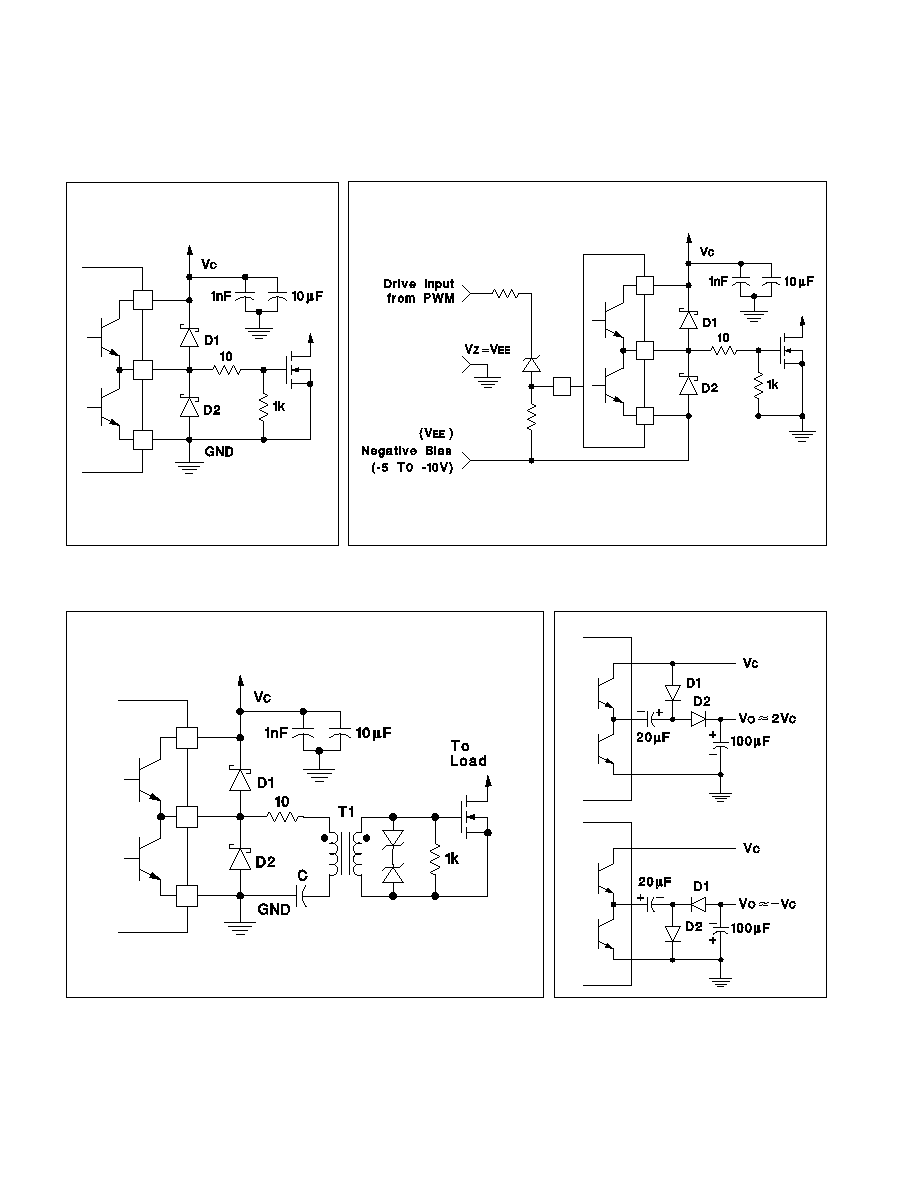
APPLICATIONS
UNITRODE CORPORATION
7 CONTINENTAL BLVD. ∑ MERRIMACK, NH 03054
TEL. 603-424-2410 ∑ FAX 603-424-3460
D1, D2: UC3611 Schottky Diodes
D1, D2: UC3611 Schottky Diodes
D1, D2: UC3611 Schottky Diodes
Transformer Coupled MOSFET Drive Circuit
Charge Pump Circuits
Power MOSFET Drive Circuit
Power MOSFET Drive Circuit using Negative Bias Voltage and Level
Shifting to Ground Referenced PWMs.
PACKAGING INFORMATION
Orderable Device
Status
(1)
Package
Type
Package
Drawing
Pins Package
Qty
Eco Plan
(2)
Lead/Ball Finish
MSL Peak Temp
(3)
5962-9579801M2A
ACTIVE
LCCC
FK
20
1
TBD
POST-PLATE
Level-NC-NC-NC
5962-9579801MPA
ACTIVE
CDIP
JG
8
1
TBD
A42 SNPB
Level-NC-NC-NC
5962-9579801VPA
ACTIVE
CDIP
JG
8
1
TBD
A42
Level-NC-NC-NC
UC1705J
ACTIVE
CDIP
JG
8
1
TBD
A42 SNPB
Level-NC-NC-NC
UC1705J883B
ACTIVE
CDIP
JG
8
1
TBD
A42 SNPB
Level-NC-NC-NC
UC1705L883B
ACTIVE
LCCC
FK
20
1
TBD
POST-PLATE
Level-NC-NC-NC
UC2705D
ACTIVE
SOIC
D
8
75
Green (RoHS &
no Sb/Br)
CU NIPDAU
Level-2-260C-1 YEAR
UC2705J
ACTIVE
CDIP
JG
8
1
TBD
A42 SNPB
Level-NC-NC-NC
UC2705N
ACTIVE
PDIP
P
8
50
Green (RoHS &
no Sb/Br)
CU NIPDAU
Level-NC-NC-NC
UC3705D
ACTIVE
SOIC
D
8
75
Green (RoHS &
no Sb/Br)
CU NIPDAU
Level-2-260C-1 YEAR
UC3705DTR
ACTIVE
SOIC
D
8
2500 Green (RoHS &
no Sb/Br)
CU NIPDAU
Level-2-260C-1 YEAR
UC3705DTRG4
ACTIVE
SOIC
D
8
2500 Green (RoHS &
no Sb/Br)
CU NIPDAU
Level-2-260C-1 YEAR
UC3705J
ACTIVE
CDIP
JG
8
1
TBD
A42 SNPB
Level-NC-NC-NC
UC3705N
ACTIVE
PDIP
P
8
50
Green (RoHS &
no Sb/Br)
CU NIPDAU
Level-NC-NC-NC
UC3705NG4
ACTIVE
PDIP
P
8
50
Green (RoHS &
no Sb/Br)
CU NIPDAU
Level-NC-NC-NC
UC3705T
ACTIVE
TO-220
KC
5
50
Green (RoHS &
no Sb/Br)
CU SN
Level-NC-NC-NC
UC3705TG3
ACTIVE
TO-220
KC
5
50
Green (RoHS &
no Sb/Br)
CU SN
Level-NC-NC-NC
(1)
The marketing status values are defined as follows:
ACTIVE: Product device recommended for new designs.
LIFEBUY: TI has announced that the device will be discontinued, and a lifetime-buy period is in effect.
NRND: Not recommended for new designs. Device is in production to support existing customers, but TI does not recommend using this part in
a new design.
PREVIEW: Device has been announced but is not in production. Samples may or may not be available.
OBSOLETE: TI has discontinued the production of the device.
(2)
Eco
Plan
-
The
planned
eco-friendly
classification:
Pb-Free
(RoHS)
or
Green
(RoHS
&
no
Sb/Br)
-
please
check
http://www.ti.com/productcontent
for the latest availability information and additional product content details.
TBD: The Pb-Free/Green conversion plan has not been defined.
Pb-Free (RoHS): TI's terms "Lead-Free" or "Pb-Free" mean semiconductor products that are compatible with the current RoHS requirements
for all 6 substances, including the requirement that lead not exceed 0.1% by weight in homogeneous materials. Where designed to be soldered
at high temperatures, TI Pb-Free products are suitable for use in specified lead-free processes.
Green (RoHS & no Sb/Br): TI defines "Green" to mean Pb-Free (RoHS compatible), and free of Bromine (Br) and Antimony (Sb) based flame
retardants (Br or Sb do not exceed 0.1% by weight in homogeneous material)
(3)
MSL, Peak Temp. -- The Moisture Sensitivity Level rating according to the JEDEC industry standard classifications, and peak solder
temperature.
Important Information and Disclaimer:The information provided on this page represents TI's knowledge and belief as of the date that it is
provided. TI bases its knowledge and belief on information provided by third parties, and makes no representation or warranty as to the
accuracy of such information. Efforts are underway to better integrate information from third parties. TI has taken and continues to take
reasonable steps to provide representative and accurate information but may not have conducted destructive testing or chemical analysis on
incoming materials and chemicals. TI and TI suppliers consider certain information to be proprietary, and thus CAS numbers and other limited
PACKAGE OPTION ADDENDUM
www.ti.com
18-Oct-2005
Addendum-Page 1

information may not be available for release.
In no event shall TI's liability arising out of such information exceed the total purchase price of the TI part(s) at issue in this document sold by TI
to Customer on an annual basis.
PACKAGE OPTION ADDENDUM
www.ti.com
18-Oct-2005
Addendum-Page 2
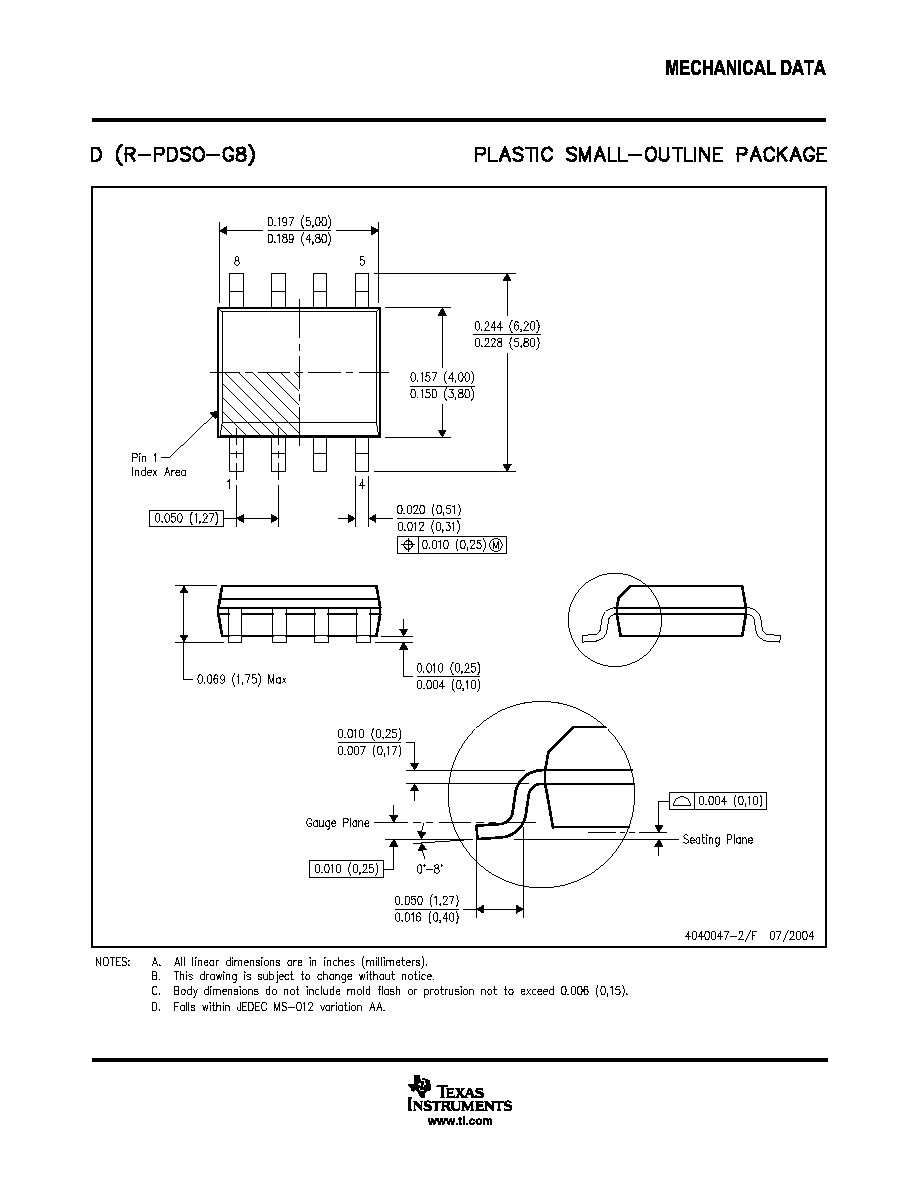
MECHANICAL DATA
MCER001A ≠ JANUARY 1995 ≠ REVISED JANUARY 1997
POST OFFICE BOX 655303
∑
DALLAS, TEXAS 75265
JG (R-GDIP-T8)
CERAMIC DUAL-IN-LINE
0.310 (7,87)
0.290 (7,37)
0.014 (0,36)
0.008 (0,20)
Seating Plane
4040107/C 08/96
5
4
0.065 (1,65)
0.045 (1,14)
8
1
0.020 (0,51) MIN
0.400 (10,16)
0.355 (9,00)
0.015 (0,38)
0.023 (0,58)
0.063 (1,60)
0.015 (0,38)
0.200 (5,08) MAX
0.130 (3,30) MIN
0.245 (6,22)
0.280 (7,11)
0.100 (2,54)
0
∞
≠15
∞
NOTES: A. All linear dimensions are in inches (millimeters).
B. This drawing is subject to change without notice.
C. This package can be hermetically sealed with a ceramic lid using glass frit.
D. Index point is provided on cap for terminal identification.
E. Falls within MIL STD 1835 GDIP1-T8
MECHANICAL DATA
MLCC006B ≠ OCTOBER 1996
POST OFFICE BOX 655303
∑
DALLAS, TEXAS 75265
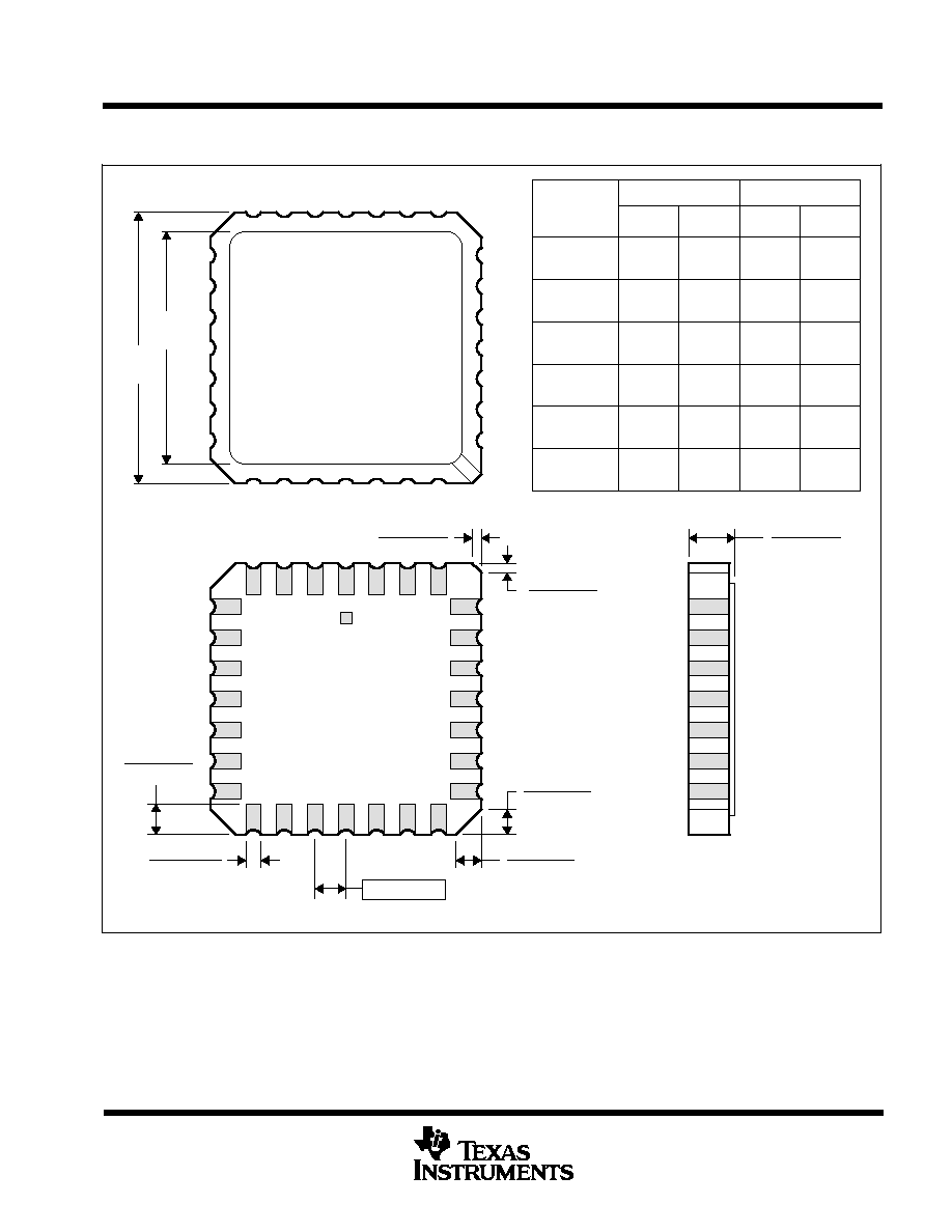
FK (S-CQCC-N**)
LEADLESS CERAMIC CHIP CARRIER
4040140 / D 10/96
28 TERMINAL SHOWN
B
0.358
(9,09)
MAX
(11,63)
0.560
(14,22)
0.560
0.458
0.858
(21,8)
1.063
(27,0)
(14,22)
A
NO. OF
MIN
MAX
0.358
0.660
0.761
0.458
0.342
(8,69)
MIN
(11,23)
(16,26)
0.640
0.739
0.442
(9,09)
(11,63)
(16,76)
0.962
1.165
(23,83)
0.938
(28,99)
1.141
(24,43)
(29,59)
(19,32)
(18,78)
**
20
28
52
44
68
84
0.020 (0,51)
TERMINALS
0.080 (2,03)
0.064 (1,63)
(7,80)
0.307
(10,31)
0.406
(12,58)
0.495
(12,58)
0.495
(21,6)
0.850
(26,6)
1.047
0.045 (1,14)
0.045 (1,14)
0.035 (0,89)
0.035 (0,89)
0.010 (0,25)
12
13
14
15
16
18
17
11
10
8
9
7
5
4
3
2
0.020 (0,51)
0.010 (0,25)
6
1
28
26
27
19
21
B SQ
A SQ
22
23
24
25
20
0.055 (1,40)
0.045 (1,14)
0.028 (0,71)
0.022 (0,54)
0.050 (1,27)
NOTES: A. All linear dimensions are in inches (millimeters).
B. This drawing is subject to change without notice.
C. This package can be hermetically sealed with a metal lid.
D. The terminals are gold plated.
E. Falls within JEDEC MS-004
MECHANICAL DATA
MPDI001A ≠ JANUARY 1995 ≠ REVISED JUNE 1999
POST OFFICE BOX 655303
∑
DALLAS, TEXAS 75265
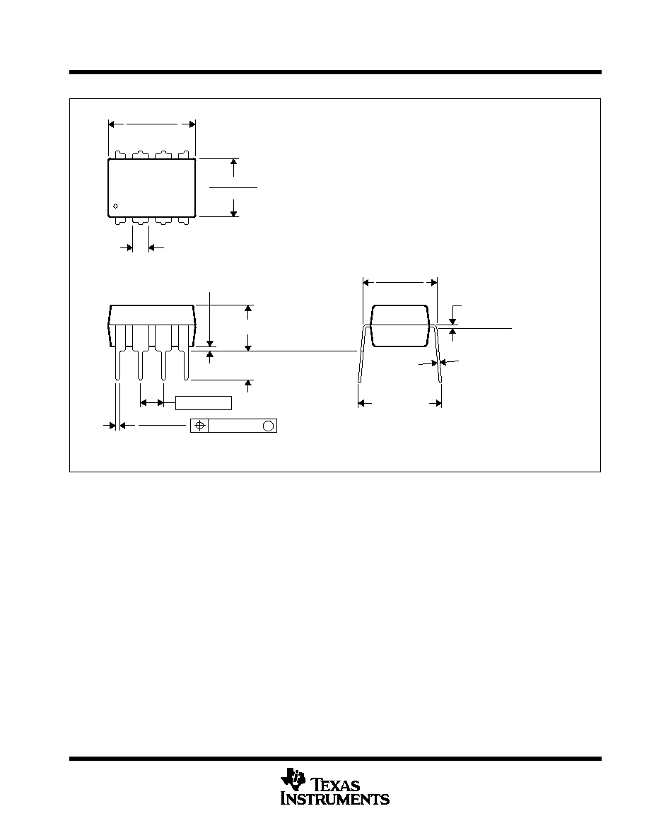
P (R-PDIP-T8)
PLASTIC DUAL-IN-LINE
8
4
0.015 (0,38)
Gage Plane
0.325 (8,26)
0.300 (7,62)
0.010 (0,25) NOM
MAX
0.430 (10,92)
4040082/D 05/98
0.200 (5,08) MAX
0.125 (3,18) MIN
5
0.355 (9,02)
0.020 (0,51) MIN
0.070 (1,78) MAX
0.240 (6,10)
0.260 (6,60)
0.400 (10,60)
1
0.015 (0,38)
0.021 (0,53)
Seating Plane
M
0.010 (0,25)
0.100 (2,54)
NOTES: A. All linear dimensions are in inches (millimeters).
B. This drawing is subject to change without notice.
C. Falls within JEDEC MS-001
For the latest package information, go to http://www.ti.com/sc/docs/package/pkg_info.htm
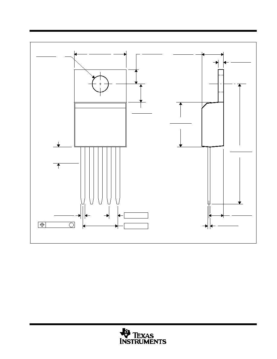
MECHANICAL DATA
MSOT008B ≠ JANUARY 1995 ≠ REVISED SEPTEMBER 2000
1
POST OFFICE BOX 655303
∑
DALLAS, TEXAS 75265
KC (R-PSFM-T5)
PLASTIC FLANGE-MOUNT
4040208/E 09/00
0.420 (10,67)
0.185 (4,70)
0.055 (1,40)
0.147 (3,73)
0.340 (8,64)
1.037 (26,34)
0.040 (1,02)
0.030 (0,76)
0.997 (25,32)
0.380 (9,65)
0.330 (8,38)
0.137 (3,48)
0.045 (1,14)
0.175 (4,46)
0.113 (2,87)
0.122 (3,10)
0.025 (0,64)
0.102 (2,59)
0.012 (0,30)
0.103 (2,62)
0.146 (3,71)
0.156 (3,96)
DIA
(see Note C)
0.125 (3,18)
0.067 (1,70)
0.268 (6,81)
5
1
M
0.010 (0,25)
NOTES: A. All linear dimensions are in inches (millimeters).
B. This drawing is subject to change without notice.
C. Lead dimensions are not controlled within this area.
D. All lead dimensions apply before solder dip.
E. The center lead is in electrical contact with the mounting tab.

IMPORTANT NOTICE
Texas Instruments Incorporated and its subsidiaries (TI) reserve the right to make corrections, modifications,
enhancements, improvements, and other changes to its products and services at any time and to discontinue
any product or service without notice. Customers should obtain the latest relevant information before placing
orders and should verify that such information is current and complete. All products are sold subject to TI's terms
and conditions of sale supplied at the time of order acknowledgment.
TI warrants performance of its hardware products to the specifications applicable at the time of sale in
accordance with TI's standard warranty. Testing and other quality control techniques are used to the extent TI
deems necessary to support this warranty. Except where mandated by government requirements, testing of all
parameters of each product is not necessarily performed.
TI assumes no liability for applications assistance or customer product design. Customers are responsible for
their products and applications using TI components. To minimize the risks associated with customer products
and applications, customers should provide adequate design and operating safeguards.
TI does not warrant or represent that any license, either express or implied, is granted under any TI patent right,
copyright, mask work right, or other TI intellectual property right relating to any combination, machine, or process
in which TI products or services are used. Information published by TI regarding third-party products or services
does not constitute a license from TI to use such products or services or a warranty or endorsement thereof.
Use of such information may require a license from a third party under the patents or other intellectual property
of the third party, or a license from TI under the patents or other intellectual property of TI.
Reproduction of information in TI data books or data sheets is permissible only if reproduction is without
alteration and is accompanied by all associated warranties, conditions, limitations, and notices. Reproduction
of this information with alteration is an unfair and deceptive business practice. TI is not responsible or liable for
such altered documentation.
Resale of TI products or services with statements different from or beyond the parameters stated by TI for that
product or service voids all express and any implied warranties for the associated TI product or service and
is an unfair and deceptive business practice. TI is not responsible or liable for any such statements.
Following are URLs where you can obtain information on other Texas Instruments products and application
solutions:
Products
Applications
Amplifiers
amplifier.ti.com
Audio
www.ti.com/audio
Data Converters
dataconverter.ti.com
Automotive
www.ti.com/automotive
DSP
dsp.ti.com
Broadband
www.ti.com/broadband
Interface
interface.ti.com
Digital Control
www.ti.com/digitalcontrol
Logic
logic.ti.com
Military
www.ti.com/military
Power Mgmt
power.ti.com
Optical Networking
www.ti.com/opticalnetwork
Microcontrollers
microcontroller.ti.com
Security
www.ti.com/security
Telephony
www.ti.com/telephony
Video & Imaging
www.ti.com/video
Wireless
www.ti.com/wireless
Mailing Address:
Texas Instruments
Post Office Box 655303 Dallas, Texas 75265
Copyright
2005, Texas Instruments Incorporated