 | –≠–ª–µ–∫—Ç—Ä–æ–Ω–Ω—ã–π –∫–æ–º–ø–æ–Ω–µ–Ω—Ç: UC2708 | –°–∫–∞—á–∞—Ç—å:  PDF PDF  ZIP ZIP |
Document Outline
- Application Notes
- Design Notes
3/97
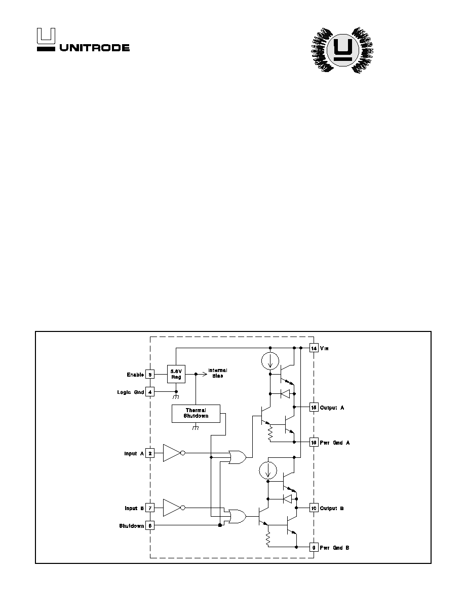
BLOCK DIAGRAM
∑
3.0A Peak Current Totem Pole
Output
∑
5 to 35V Operation
∑
25ns Rise and Fall Times
∑
25ns Propagation Delays
∑
Thermal Shutdown and Under-
Voltage Protection
∑
High-Speed, Power MOSFET
Compatible
∑
Efficient High Frequency Operation
∑
Low Cross-Conduction Current Spike
∑
Enable and Shutdown Functions
∑
Wide Input Voltage Range
∑
ESD Protection to 2kV
The UC1708 family of power drivers is made with a high-speed, high-
voltage, Schottky process to interface control functions and high-power
switching devices ≠ particularly power MOSFETs. Operating over a 5 to
35 volt supply range, these devices contain two independent channels.
The A and B inputs are compatible with TTL and CMOS logic families,
but can withstand input voltages as high as V
IN
. Each output can source
or sink up to 3A as long as power dissipation limits are not exceeded.
Although each output can be activated independently with its own inputs,
they can be forced low in common through the action of either a digital
high signal at the Shutdown terminal or by forcing the Enable terminal
low. The Shutdown terminal will only force the outputs low, it will not ef-
fect the behavior of the rest of the device. The Enable terminal effectively
places the device in under-voltage lockout, reducing power consumption
by as much as 90%. During under-voltage and disable (Enable terminal
forced low) conditions, the outputs are held in a self-biasing, low-voltage,
state.
The UC3708 and UC2708 are available in plastic 8-pin MINIDIP and 16-
pin "bat-wing" DIP packages for commercial operation over a 0
o
C to
+70
o
C temperature range and industrial temperature range of -25
o
C to
+85
o
C respectively. For operation over a -55
o
C to +125
o
C temperature
range, the UC1708 is available in hermetically sealed 8-pin MINIDIP and
16 pin DIP packages. Surface mount devices are also available.
UC1708
UC2708
UC3708
Dual Non-Inverting Power Driver
Note: Shutdown feature available only in JE , NE or DW packages.
UDG-92024-1
FEATURES
DESCRIPTION
1
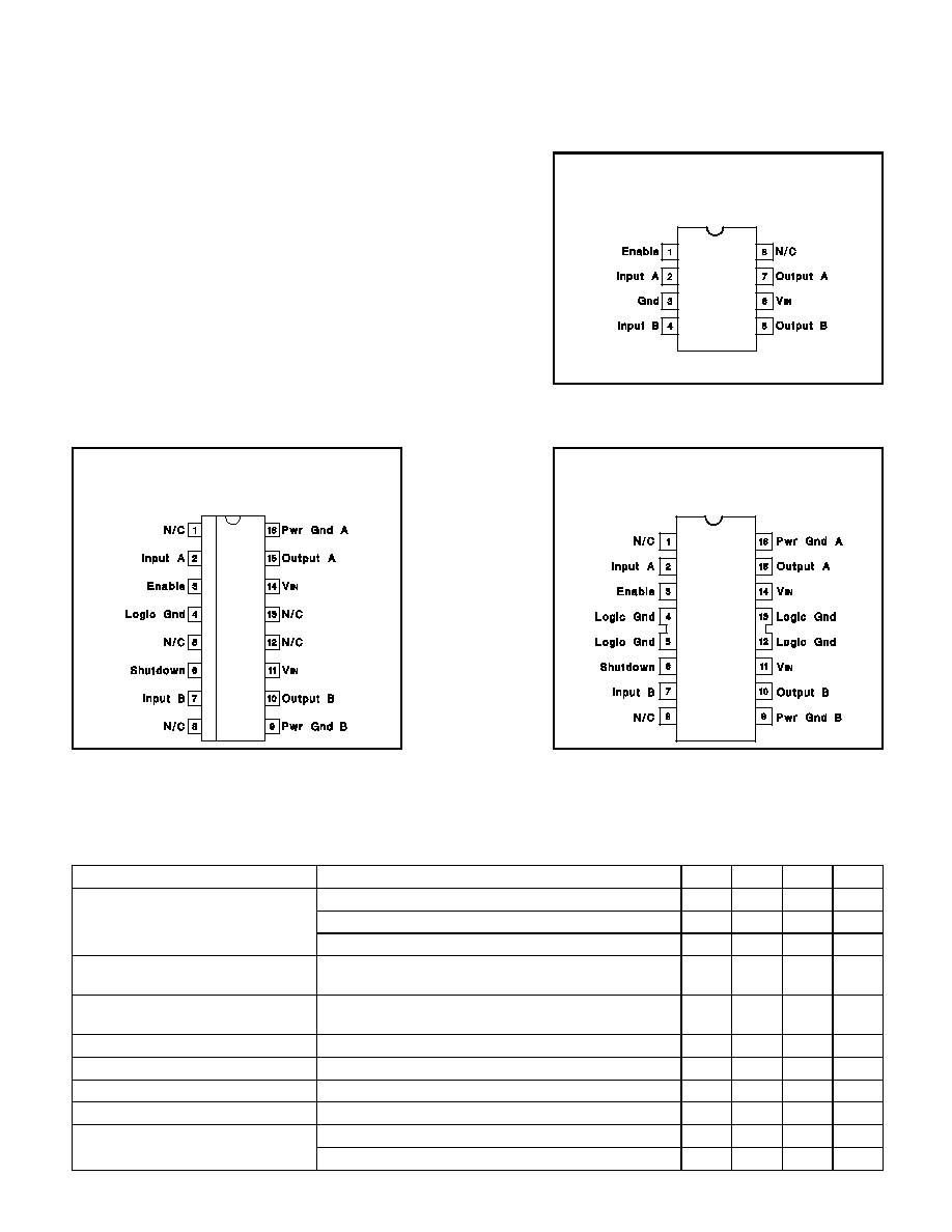
CONNECTION DIAGRAMS
Supply Voltage V
IN
. . . . . . . . . . . . . . . . . . . . . . . . . . . . . . . . 35V
Output Current (Each Output, Source or Sink)
Steady-State . . . . . . . . . . . . . . . . . . . . . . . . . . . . . . . . . . 0.5A
Peak Transient . . . . . . . . . . . . . . . . . . . . . . . . . . . . . . . . . . 3A
Ouput Voltage . . . . . . . . . . . . . . . . . . . . . . .
-
0.3 to (V
IN
+ 0.3)V
Enable and Shutdown Inputs . . . . . . . . . . . . . . . . .
-
0.3 to 6.2V
A and B Inputs . . . . . . . . . . . . . . . . . . . . . . .
-
0.3 to (V
IN
+ 0.3)V
Operating Junction Temperature (Note 2) . . . . . . . . . . . . 150
∞
C
Storage Temperature Range . . . . . . . . . . . . . . . . -65
∞
to 150
∞
C
Lead Temperature (Soldering, 10 Seconds) . . . . . . . . . . 300
∞
C
ABSOLUTE MAXIMUM RATINGS (Note 1)
UC1708
UC2708
UC3708
NOTE 1: All voltages are with respect to Logic Gnd pin. All cur-
rents are positive into, negative out of, device terminals.
NOTE 2: Consult Unitrode Integrated Circuits databook for
information regarding thermal specifications and limitations of
packages.
PARAMETER
TEST CONDITIONS
MIN
TYP
MAX
UNITS
V
IN
Supply Current
OutputsLow
18
26
mA
Outputs High
14
18
mA
Enable = 0V
1
4
mA
A, B and Shutdown Inputs Low
Level
0.8
V
A, B and Shutdown Inputs High
Level
2.0
V
A, B Input Current Low
V
A,B
= 0.4V
-1
-0.6
mA
A, B Input Current High
V
A,B
= 2.4V
-200
50
µ
A
A, B Input Leakage Current High
V
A,B
= 35.3V
200
µ
A
Shutdown Input Current Low
V
SHUTDOWN
= 0.4V
20
100
µ
A
Shutdown Input Current High
V
SHUTDOWN
= 2.4V
170
500
µ
A
V
SHUTDOWN
= 6.2V
0.6
1.5
mA
ELECTRICAL CHARACTERISTICS:
Unless otherwise stated, V
IN
=10V to 35V, and these specifications apply for:
≠55
o
C<T
A
<125
o
C for the UC1708, ≠25
o
C<T
A
<+85
o
C for the UC2708, and 0
o
C<T
A
<70
o
C for the UC3708. T
A
= T
J.
DIL-8 (Top View)
J Or N Package
Note: In JE package Pin 4 is logic ground. Pins 5, 12,
and 13 are N/C.
DIL-16 (Top View)
JE or NE Package
SOIC-16 (Top View)
DW Package
2
UC1708
UC2708
UC3708
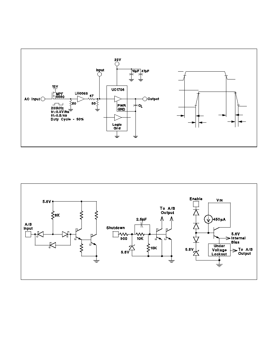
SWITCHING CHARACTERISTICS (Figure 1)
(V
IN
= 20V, delays measured to 10% output change.)
PARAMETER
TEST CONDITIONS
MIN
TYP
MAX
UNITS
From A,B Input to Output:
Rise Time Delay (TPLH)
CL = 0pF
25
40
ns
CL = 1000pF (Note 3)
25
40
ns
CL = 2200pF
30
45
ns
10% to 90% Rise (TTLH)
CL = 0pF
55
75
ns
CL = 1000pF (Note 3)
25
50
ns
CL = 2200pF
40
55
ns
Fall Time Delay (TPHL)
CL = 0pF
25
40
ns
CL = 1000pF (Note 3)
25
45
ns
CL = 2200pF
35
50
ns
90% to 10% Fall (TTHL)
CL = 0pF
15
20
ns
CL = 1000pF (Note 3)
25
45
ns
CL = 2200pF
40
55
ns
From Shutdown Input to Output
Rise Time Delay (TPLH)
CL = 0pF
25
75
ns
CL = 1000pF (Note 3)
30
75
ns
CL = 2200pF
35
75
ns
10% to 90% Rise (TTLH)
CL = 0pf
50
75
ns
CL = 1000pF (Note 3)
25
50
ns
CL = 2200pF
40
55
ns
Fall Time Delay (TPHL)
CL = 0pF
25
45
ns
CL = 1000pF (Note 3)
30
50
ns
CL = 2200pF
35
55
ns
90% to 10% Fall (TTHL)
CL = 0pF
25
20
ns
CL = 1000pF (Note 3)
25
45
ns
CL = 2200pF
40
55
ns
Total Supply Current
F = 200kHz, 50% duty cycle, both channels; CL = 0pF
23
25
mA
F = 200kHz, 50% duty cycle, both channels; CL = 2200pF
38
45
mA
NOTE 3: These parameters, specified at 1000pF, although guaranteed over recommended operating conditions, are not tested in
production.
PARAMETER
TEST CONDITIONS
MIN
TYP
MAX
UNITS
Enable Input Current Low
V
ENABLE
= 0V
-600
-460
200
µ
A
Enable Input Current High
V
ENABLE
= 6.2V
200
µ
A
Enable Threshold Rising
2.8
3.6
V
Enable Threshold Falling
1.0
2.4
3.4
V
Output High Sat., V
IN
- V
OUT
I
OUT
= -50mA
2.0
V
I
OUT
= -500mA
2.5
V
Output Low Sat., V
OUT
I
OUT
= 50mA
0.5
V
I
OUT
= 500mA
2.5
V
Thermal Shutdown
155
∞
C
ELECTRICAL CHARACTERISTICS (cont.):
Unless otherwise stated, V
IN
= 10V to 35V, and these specifications apply
for: ≠55
o
C<T
A
<125
o
C for the UC1708, ≠25
o
C<T
A
<+85
o
C for the UC2708, and 0
o
C<T
A
<70
o
C for the UC3708. T
A
= T
J.
3
Note: Shutdown feature available only in JE, NE or DW Packages.
UNITRODE CORPORATION
7 CONTINENTAL BLVD.
∑
MERRIMACK, NH 03054
TEL. (603) 424-2410
∑
FAX (603) 424-3460
Figure 2: Equivalent Input Circuits
4.3V
0V
20V
0V
INPUT
90%
50%
10%
OUTPUT
90%
10%
50%
TP
TP
TT
TT
LH
LH
HL
HL
Figure 1: AC Test Circuit and Switching Time Waveforms
UDG-92025
UDG-92026
UC1708
UC2708
UC3708
4

IMPORTANT NOTICE
Texas Instruments and its subsidiaries (TI) reserve the right to make changes to their products or to discontinue
any product or service without notice, and advise customers to obtain the latest version of relevant information
to verify, before placing orders, that information being relied on is current and complete. All products are sold
subject to the terms and conditions of sale supplied at the time of order acknowledgement, including those
pertaining to warranty, patent infringement, and limitation of liability.
TI warrants performance of its semiconductor products to the specifications applicable at the time of sale in
accordance with TI's standard warranty. Testing and other quality control techniques are utilized to the extent
TI deems necessary to support this warranty. Specific testing of all parameters of each device is not necessarily
performed, except those mandated by government requirements.
CERTAIN APPLICATIONS USING SEMICONDUCTOR PRODUCTS MAY INVOLVE POTENTIAL RISKS OF
DEATH, PERSONAL INJURY, OR SEVERE PROPERTY OR ENVIRONMENTAL DAMAGE ("CRITICAL
APPLICATIONS"). TI SEMICONDUCTOR PRODUCTS ARE NOT DESIGNED, AUTHORIZED, OR
WARRANTED TO BE SUITABLE FOR USE IN LIFE-SUPPORT DEVICES OR SYSTEMS OR OTHER
CRITICAL APPLICATIONS. INCLUSION OF TI PRODUCTS IN SUCH APPLICATIONS IS UNDERSTOOD TO
BE FULLY AT THE CUSTOMER'S RISK.
In order to minimize risks associated with the customer's applications, adequate design and operating
safeguards must be provided by the customer to minimize inherent or procedural hazards.
TI assumes no liability for applications assistance or customer product design. TI does not warrant or represent
that any license, either express or implied, is granted under any patent right, copyright, mask work right, or other
intellectual property right of TI covering or relating to any combination, machine, or process in which such
semiconductor products or services might be or are used. TI's publication of information regarding any third
party's products or services does not constitute TI's approval, warranty or endorsement thereof.
Copyright
©
1999, Texas Instruments Incorporated