UC1709, UC2709, UC3709
DUAL HIGH- SPEED FET DRIVER
SLUS196A -- NOVEMBER 1996 -- REVISED MARCH 2000
1
POST OFFICE BOX 655303
∑
DALLAS, TEXAS 75265
D
1.5 Amp Source/Sink Drive
D
Pin Compatible with 0026 Products
D
40 ns Rise and Fall into 1000pF
D
Low Quiescent Current
D
5 V to 40 V Operation
D
Thermal Protection
description
The UC3709 family of power drivers is an
effective low-cost solution to the problem of
providing fast turn-on and off for the
capacitive gates of power MOSFETs. Made
with a high-speed Schottky process, these
devices will provide up to 1.5 A of either
source or sink current from a totem--pole
output stage configured for minimal
cross-conduction current spike.
The UC3709 is pin compatible with the
MMH0026 or DS0026, and while the delay
times are longer, the supply current is much
less than these older devices.
With inverting logic, these units feature complete TTL compatibility at the inputs with an output stage that can
swing over 30 V. This design also includes thermal shutdown protection.
absolute maximum ratings over operating free-air temperature range (unless otherwise noted)
}}}}
N--Pkg
J--Pkg
Supply Voltage, V
CC
40 V
40V
. . . . . . . . . . . . . . . . . . . . . . . . . . . . . . . . . . . . . . . . . . .
. . . . . . . . . . . . . . . . . . . . . . .
Output Current (Source or Sink)
Steady--State
±500 mA
±500 mA
. . . . . . . . . . . . . . . . . . . . . . . . . . . . . . . . . . . . . . . . . . .
. . . . . . . . . . . . . . . . . . .
Peak Transient
±1.5 A
±1.0 A
. . . . . . . . . . . . . . . . . . . . . . . . . . . . . . . . . . . . . . . . . . . .
. . . . . . . . . . . . . . . . . . . . .
Capacitive Discharge Energy
20 mJ
15 mJ
. . . . . . . . . . . . . . . . . . . . . . . . . . . . . . . .
. . . . . . . . . . . . . . . . . . . . . .
Digital Inputs}
5.5 V
5.5 V
. . . . . . . . . . . . . . . . . . . . . . . . . . . . . . . . . . . . . . . . . . . . . . . .
. . . . . . . . . . . . . . . . . . . . . .
Power Dissipation at T
A
= 25∞C
1 W
1 W
. . . . . . . . . . . . . . . . . . . . . . . . . . . . . . . . . .
. . . . . . . . . . . . . . . . . . . . . . .
Power Dissipation at T
C
= 25∞C
3 W
2 W
. . . . . . . . . . . . . . . . . . . . . . . . . . . . . . . . . .
. . . . . . . . . . . . . . . . . . . . . . .
Operating Temperature Range
--55∞C to 125∞C
--55∞C to 125∞C
. . . . . . . . . . . . . . . . . . . . . . . . .
. . . . . . . . . . . . .
Storage Temperature Range
--65∞C to 150∞C
--65∞C to 150∞C
. . . . . . . . . . . . . . . . . . . . . . . . . .
. . . . . . . . . . . . .
Lead Temperature (Soldering, 10 Seconds)
300∞C
300 ∞C
. . . . . . . . . . . . . . . . . . . . . .
. . . . . . . . . . . . . . . . . . . . .
Stresses beyond those listed under "absolute maximum ratings" may cause permanent damage to the device. These are stress ratings only, and
functional operation of the device at these or any other conditions beyond those indicated under "recommended operating conditions" is not
implied. Exposure to absolute-maximum-rated conditions for extended periods may affect device reliability.
All currents are positive into and negative out of the specified terminals. Digital drive can exceed 5.5V if input is limited to 10A. Consult the
Packaging Section of the Databook for thermal limitations and considerations of the package.
Copyright „ 2000, Texas Instruments Incorporated
PRODUCTION DATA information is current as of publication date.
Products conform to specifications per the terms of Texas Instruments
standard warranty. Production processing does not necessarily include
testing of all parameters.
Please be aware that an important notice concerning availability, standard warranty, and use in critical applications of
Texas Instruments semiconductor products and disclaimers thereto appears at the end of this data sheet.
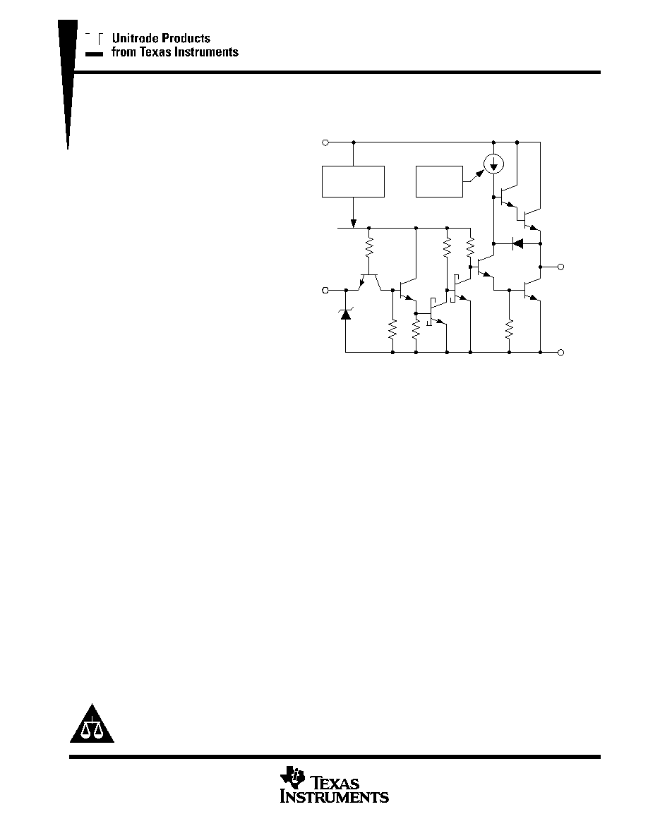
simplified schematic (only one driver shown)
5 VOLT
REGULATOR
THERMAL
SENSE
6 k
5.6 V
INPUT
A OR B
INPUT
A OR B
GND
V
CC
UDG--00068
UC1709, UC2709, UC3709
DUAL HIGH- SPEED FET DRIVER
SLUS196A -- NOVEMBER 1996 -- REVISED MARCH 2000
2
POST OFFICE BOX 655303
∑
DALLAS, TEXAS 75265
1
2
3
4
8
7
6
5
N/C
INPUT A
GROUND
INPUT B
N/C
OUTPUT A
V
CC
OUTPUT B
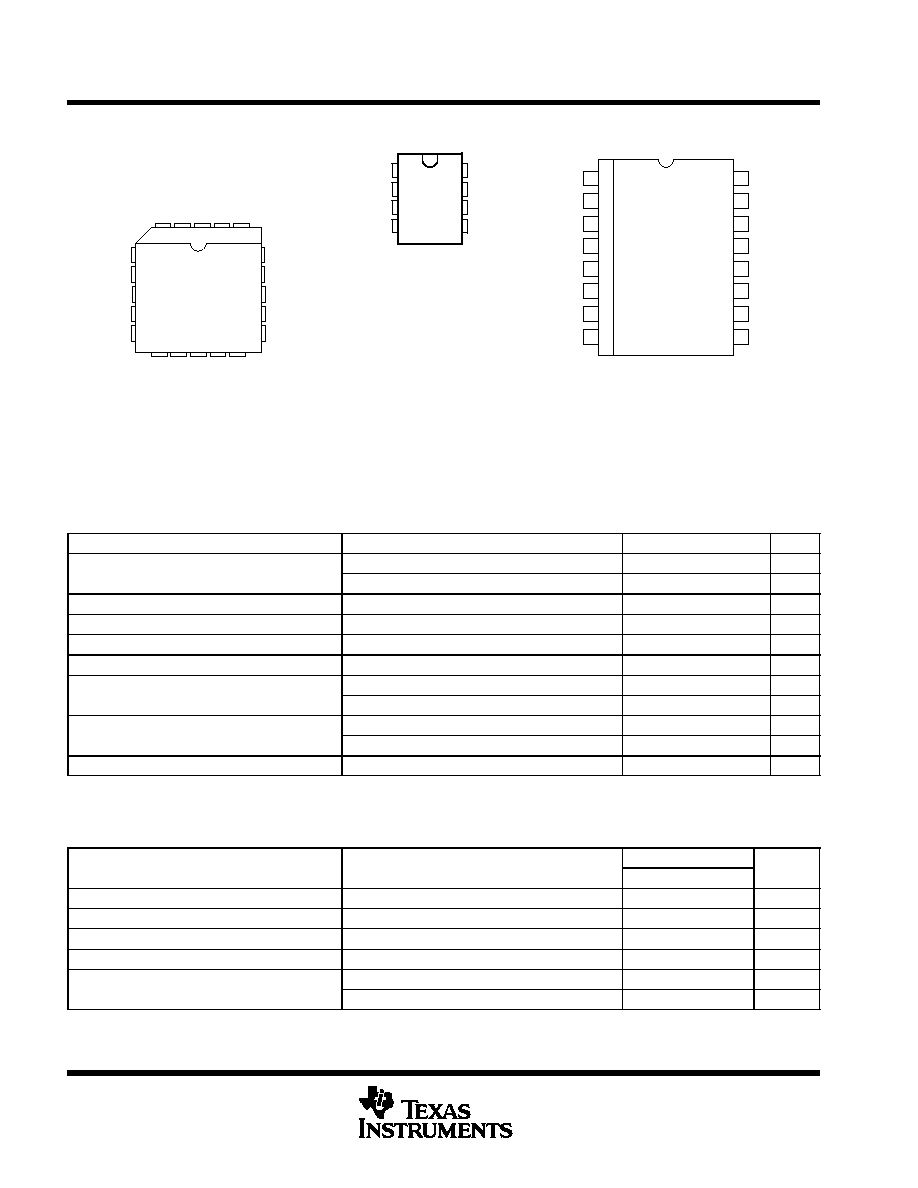
8 PIN DIL N OR J PACKAGE
(TOP VIEW)
N/C -- No internal connection
V
CC
N/C
N/C
N/C
OUTPUT B
INPUT B
1
2
3
4
5
6
7
8
16
15
14
13
12
11
N/C
N/C
GROUND
INPUT A
N/C
N/C
OUTPUT A
N/C
N/C
N/C
10
9
SOIC--16 (TOP VIEW)
DW PACKAGE
PLCC--20, LCC--20 (TOP VIEW)
Q, L PACKAGES
3
18
17
16
N/C
1
2
20 19
15
14
4
5
6
7
8
9
11
10
12 13
N/C
INP
U
T
A
OUT
P
UT
A
N/C
N/C
N/C
V
CC
N/C
N/C
N/C
N/C
GROUND
N/C
N/C
N/C
OU
T
P
U
T
B
N/C
INP
U
T
B
N/C
electrical characteristics over recommended operating free-air temperature range, T
A
= 55∞∞∞∞C to
125∞∞∞∞C for the UC1709, --40∞∞∞∞C to 85∞∞∞∞C for the UC2709, and 0∞∞∞∞C to 70∞∞∞∞C for the UC3709;
V
CC
= 20 V, T
A
= T
J.
PARAMETER
TEST CONDITIONS
MIN
TYP
MAX
UNIT
Supply current
Both outputs low
10
12
mA
Supply current
Both outputs high
7
10
mA
Logic 0 input voltage
0.8
V
Logic 1 input voltage
2.2
V
Input current
V
I
= 0
--0.6
--1.0
mA
Input leakage
V
I
= 5 V
0.05
0.1
mA
Output high saturation V
V
I
O
= --50 mA
1.5
2.0
V
Output high saturation V
CC
--V
O
I
O
= --500 mA
2.0
2.5
V
Output low saturation V
I
O
= 50 mA
0.1
0.4
V
Output low saturation V
O
I
O
= 500 mA
2.0
2.5
V
Thermal shutdown
155
mA
typical switching characteristics, V
CC
= 20 V, T
A
= 25∞∞∞∞C, delays measured to 10% output change
PARAMETER
TEST CONDITIONS
OUTPUT C
L
=
UNITS
PARAMETER
TEST CONDITIONS
0 nF
2.2 nF
UNITS
Rise time delay
80
80
ns
10% to 90% rise
20
40
ns
Fall time delay
60
80
ns
10% to 90% fall
20
40
ns
VCC cross--conduction
Output rise
25
ns
VCC cross--conduction
curent spike duration
Output fall
0
ns
NOTE: Refer to UC1705 specifications for further information.