 | –≠–ª–µ–∫—Ç—Ä–æ–Ω–Ω—ã–π –∫–æ–º–ø–æ–Ω–µ–Ω—Ç: UC27131N | –°–∫–∞—á–∞—Ç—å:  PDF PDF  ZIP ZIP |
UC17131/2/3
UC27131/2/3
UC37131/2/3
SLUS340 - APRIL 1999
FEATURES
∑
300mA Continuous Output Current
∑
Low Side or High Side Switch
Configuration
∑
8V to 65V Operation
∑
Overload and Short Circuit Protection
∑
Power Interruption Protection
∑
+6V Regulated Voltage
∑
2mA Quiescent Current
∑
Programmable Overcurrent and
Power Interruption Protection
∑
1% to 30% Programmable Input
Comparator Hysteresis (on UC37132)
∑
Low and High Side Internal High
Current Clamps When Driving
Inductive Loads
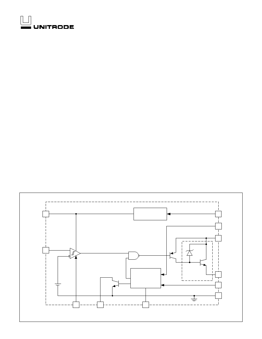
Smart Power Switch
13
12
11
VREF
IN
6
10
3
7
VCC
LS
CSH
CSL
2
GND
6V
PRE-REGULATOR
INPUT
COMPARATOR
1/2
VREF
HYST
9
LED
TURN-ON/OFF
AND
SHORT CIRCUIT
PROTECTION
4
HS
5
Q
OUT
72V
6V/8mA
CDEL
UC37132 BLOCK DIAGRAM
UDG-98026
DESCRIPTION
The UC37131, UC37132 and UC37133 are a family of smart power
switches which can drive resistive or inductive loads from the high side or
low side.
The UC37132 is available in 14 pin (DIP), 16 pin (SOIC), or 20 pin (CLCC)
packages and can accommodate both low side (load to VCC) or high side
(load to GND) configurations. The UC37131 and UC37133 are exclusively
for a low side or a high side configuration respectively and both are avail-
able in an 8 pin package. Both high side and low side configurations provide
high current switching with low saturation voltages which can drive resistive
or inductive loads.
The input to the switch is driven by a low voltage signal, typically 5V. Addi-
tionally, UC37132 features adjustable hysteresis. The output of the device
can switch a load between 8V and 65V. Output current capability is 300mA
continuous or 700mA peak.
The device also has inherent smart features that allow for programmable
turn-on delay in enabling the output following startup. The same capacitor
that specifies the turn-on delay is also used to program a VCC power inter-
ruption time. If VCC drops below a threshold for a time specified by this ca-
pacitor, the output is turned off and a new turn-on delay will be re-triggered.
Similarly, if high current persists longer than the response delay, the output
driver will operate in a very low duty cycle mode to protect the IC.
2
UC17131/2/3
UC27131/2/3
UC37131/2/3
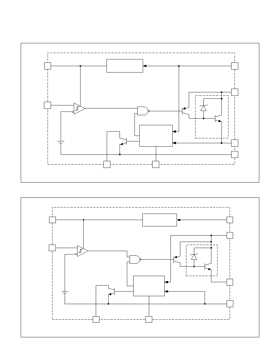
4
3
VREF
IN
2
6
8
VCC
LS
CSL
5
GND
6V
PRE-REGULATOR
INPUT
COMPARATOR
1/2
VREF
1
LED
TURN-ON/OFF
AND
SHORT CIRCUIT
PROTECTION
7
Q
OUT
72V
6V/8mA
CDEL
HYST (FIXED) =
30%
UC37131 BLOCK DIAGRAM
UDG-98059
4
3
VREF
IN
2
8
VCC
CSH
5
GND
6V
PRE-REGULATOR
INPUT
COMPARATOR
1/2
VREF
1
LED
TURN-ON/OFF
AND
SHORT CIRCUIT
PROTECTION
6
HS
7
Q
OUT
72V
6V/8mA
CDEL
HYST (FIXED) =
30%
UC37133 BLOCK DIAGRAM
UDG-98060
3
UC17131/2/3
UC27131/2/3
UC37131/2/3
HS
CSH
VCC
GND
1
2
3
4
8
7
6
5
CDEL
LED
VREF
IN
ABSOLUTE MAXIMUM RATINGS
VCC . . . . . . . . . . . . . . . . . . . . . . . . . . . . . . . . . . . . . . . . . . . 65V
LS ≠ HS (Clamped by internal circuitry) . . . . . . . . . . . . . . . 78V
CSH, LED . . . . . . . . . . . . . . . . . . . . . . . . . . . . . . . . . . . . . . 65V
Output Current
Continuous . . . . . . . . . . . . . . . . . . . . . . . . . . . . . . . . 400mA
Peak . . . . . . . . . . . . . . . . . . . . . . . . . . . . . . . . . . . . . 900mA
Remaining Pin Voltages . . . . . . . . . . . . . . . . . . . . . ≠0.3V to 9V
Storage Temperature . . . . . . . . . . . . . . . . . . .
-
65∞C to +150∞C
Junction Temperature . . . . . . . . . . . . . . . . . . . ≠55∞C to +150∞C
Lead Temperature (Soldering, 10 sec.) . . . . . . . . . . . . . +300∞C
Currents are positive into, negative out of the specified termi-
nal. Consult Packaging Section of Databook for thermal limita-
tions and considerations of packages.
PART
NUMBER
CONFIGURATIONS
PACKAGE
PIN COUNT
UCX7131
Low Side Only
8
UCX7132
Low Side or High Side
14, 16, 20
UCX7133
High Side Only
8
PRODUCT SELECTION TABLES
PART
NUMBER
TEMPERATURE
RANGE
AVAILABLE
PACKAGES
UC1713X
≠55∞C to +125∞C
J, L
UC2713X
≠40∞C to +85∞C
D, N
UC3713X
0∞C to +70∞C
D, N
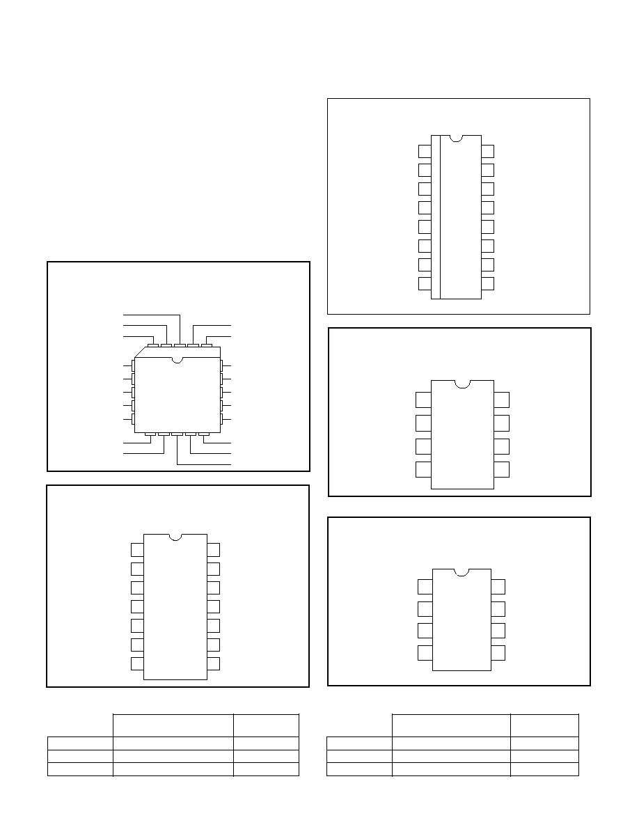
HYST
IN
N/C
VREF
CDEL
N/C
LED
1
2
3
4
5
6
7
14
13
12
11
10
9
8
GND
N/C
CSH
VCC
CSL
HS
LS
CSL
LS
VCC
GND
1
2
3
4
8
7
6
5
CDEL
LED
VREF
IN
HYST
IN
N/C
VREF
CDEL
N/C
LED
N/C
1
2
3
4
5
6
7
8
16
15
14
13
12
11
10
9
GND
N/C
VCC
CSH
N/C
CSL
HS
LS
CONNECTION DIAGRAMS
SOIC-16 (Top View)
(for UCX7132)
D Package
3
18
17
16
N/C
1
2
20 19
15
14
4
5
6
7
8
9
11
10
12 13
LS
CSH
HS
CSL
N/C
GND
N/C
N/C
IN
N/C
VCC
N/C
N/C
N/C
HYST
VREF
CDEL
N/C
LED
PLCC-20 (Top View)
(for UCX7132)
L Packages
DIL-14 (Top View)
(for UCX7132)
J, or N Packages
DIL-8, SOIC-8 (Top View)
(for UCX7131)
J, N, or D Packages
DIL-8, SOIC-8 (Top View)
(for UCX7133)
J, N, or D Packages

4
UC17131/2/3
UC27131/2/3
UC37131/2/3
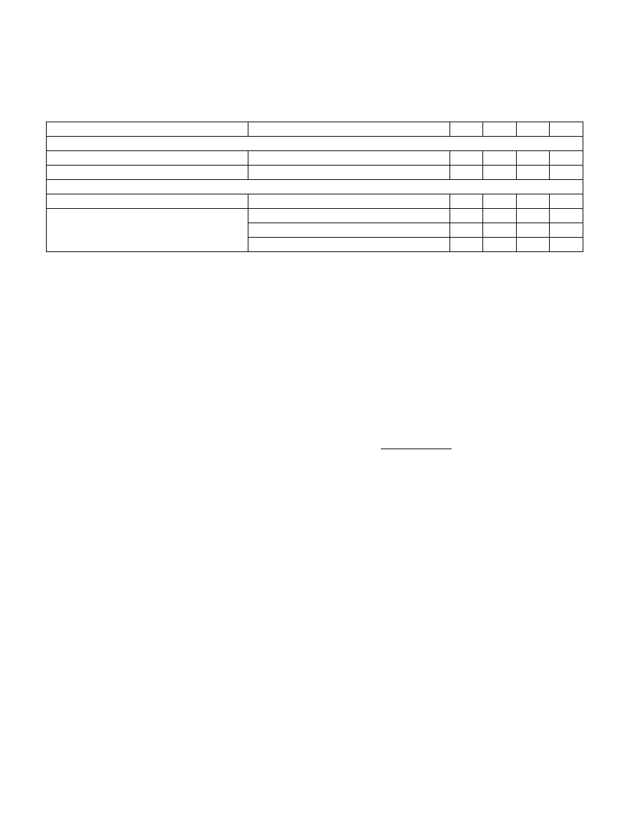
ELECTRICAL CHARACTERISTICS
Unless otherwise specified, CDEL = 10nF, VCC = 25V, CSL = GND, CSH = LS;
R
CSH
= 0.5
(Note 1); IN=0V (for OFF condition) and IN=5V (for ON condition); T
A
= T
J
.
PARAMETER
TEST CONDITIONS
MIN
TYP
MAX
UNITS
Reference
VREF
25∞C
5.8
6
6.2
V
≠55∞C to 125∞C
5.6
6
6.4
V
Line Regulation
VCC = 8V to 64V
10
35
mV
Load Regulation
0 < I
REF
< 8mA
10
50
mV
Short Circuit Current
REF = 0V
20
35
mA
Input Comparator
Turn-On Threshold Voltage
2.7
3
3.3
V
Input Bias Current
V
IN
= 3.5V
5
µ
A
Hysteresis
R
HYST
= GND (Internally for X31, X33)
0.775
0.9
1.025
V
R
HYST
= 96.67k for (X32)
30
mV
Output: High Side (UCX7133: CSH = LS and CSL = GND Internally; See Fig. 2a)
Rise Time (Off to On)
R
LOAD
= 250
to GND
30
80
V/
µ
s
Fall Time (On to Off)
R
LOAD
= 250
to GND
30
80
V/
µ
s
Output Short Circuit
HS = 0.25
to GND
500
900
mA
Voltage Clamp
LS≠HS
67
72
77
V
Saturation Voltage
25∞C, R
LOAD
= 100
to GND
1.2
V
≠40∞C, R
LOAD
= 100
to GND
1.3
V
≠55∞C, R
LOAD
= 100
to GND
1.4
V
Leakage Current
5
µ
A
Output: Low Side (UCX7131; CSH = VCC and CSL = HS Internally; See Fig. 2b)
Rise Time (On to Off)
R
LOAD
= 250
to VCC, R
CSL
= 0.5
15
50
V/
µ
s
Fall Time (Off to On)
R
LOAD
= 250
to VCC, R
CSL
= 0.5
25
60
V/
µ
s
Output Short Circuit
LS = 0.25
to VCC
500
700
900
mA
Voltage Clamp
LS≠HS
67
72
77
V
Saturation Voltage
25∞C, R
LOAD
= 100
to VCC, R
CSL
= 0.5
1.2
V
≠40∞C, R
LOAD
= 100
to VCC, R
CSL
= 0.5
1.3
V
≠55∞C, R
LOAD
= 100
to VCC, R
CSL
= 0.5
1.4
V
Leakage Current
5
µ
A
VCC Fault Section
Output Turn-On Delay, t
D(ON)
Step VCC from 0V to 8V (See Fig. 3a)
9.5
11
13.5
ms
Output Turn-Off Delay, t
D(OFF)
Pulse VCC from 25V to VCC Turn-Off
Threshold
300
500
700
µ
s
VCC Turn-Off Threshold
Pulse VCC Low
6.5
7
7.5
V
CDEL Section
V
CDEL_MAX
5.8
V
V
FAULT_H
4.9
V
V
FAULT_L
1.0
V
Overcurrent Fault Section (See Fig. 3c)
Short Circuit Turn-Off Delay, t
SC
Step I
LOAD:
0mA to 400mA
75
µ
s
Short Circuit Recovery Time, t
ROFF
I
LOAD
= 400mA, 100
µ
s
10
ms
High Side Current Threshold, I
TH-H
R
CSH
= 0.5
250
325
400
mA
Low Side Current Threshold, I
TH-L
R
CSL
= 0.5
250
325
400
mA
Overcurrent Duty Cycle
R
LOAD
= 0.25
to GND
0.6
0.8
1.0
%
5
UC17131/2/3
UC27131/2/3
UC37131/2/3
ELECTRICAL CHARACTERISTICS
Unless otherwise specified, CDEL = 10nF, VCC = 25V, CSL = GND, CSH = LS;
R
CSH
= 0.5
(Note 1); IN=0V (for OFF condition) and IN=5V (for ON condition); T
A
= T
J
.
PARAMETER
TEST CONDITIONS
MIN
TYP
MAX
UNITS
LED Output
I
SINK
, t
DOFF
, t
ROFF
V
LED
= 7V
5.0
8.0
11.0
mA
I
LEAKAGE
1
5
µ
A
Overall
Delay to Output
3
6
µ
s
ICC
Output Off
2.0
2.8
mA
I
L
= 1mA, 250mA (High Side)
2.3
3
mA
I
L
= 1mA, 250mA (Low Side)
2.5
4
mA
Note 1: All test conditions are for a high side configuration as in Fig. 2a, unless otherwise specified.
CDEL: A capacitor connected to this pin is used to pro-
gram both VCC pulse interruption time and power
turn-on delay. The capacitor discharge time corresponds
to VCC interruption and the charge time to VCC turn-on
delay. The ratio between turn-on delay and turn-off delay
will be fixed based on internal charge and discharge cur-
rents and voltage thresholds.
The same fault circuitry and capacitor is used for short
circuit and overload protection. If an overcurrent or short
circuit is detected, the capacitor starts charging and
turns off the output if the condition persists at the end of
its charge time. The output will then operate in a low-duty
cycle mode to protect the IC. After short circuit recovery,
the output will be reactivated in order to check if the short
circuit was removed. If the overcurrent persists the chip
will continue in this pulsing mode.
CSH: (For UC37132 and UC37133) This high side cur-
rent sense pin is used to program the current limit for
high side applications by connecting a resistor between
VCC and CSH. An over load current is detected when
the voltage drop between VCC and CSH exceeds
150mV. For the UC37132, in a high side application, the
CSH pin must be tied to the LS pin; in a low side applica-
tion, the CSH pin must be tied to VCC
CSL: (For UC37131 and UC37132) This low side cur-
rent sense pin is used to program the current limit for low
side applications by connecting a resistor between CSL
and GND. An over load current is detected when the volt-
age drop between CSL and GND exceeds 150mV. For
the UC37132, in a high side application, the CSL pin
must be tied to GND; in a low side application, the CSL
pin must be tied to the HS pin.
GND: The reference point for the internal reference, all
thresholds, and the return for the remainder of the de-
vice.
HS: (For UC37132 and UC37133) The output of the
switching transistor in the high side configuration. The
emitter of the output transistor is the HS pin which is con-
nected to the load. For the UC37132, the HS pin must be
tied to the CSL pin in a low side application.
HYST: (For UC37132) The pin used to program the in-
put comparator hysteresis by connecting a resistor to
ground. The hysteresis defaults to 30% with HYST
grounded (internally for UC37131 and UC37133).
V
R
HYST
HYST
=
+
3000
3330
(
)
IN: The input to the comparator that detects when the
output transistor should be turned on. The input thresh-
old is 3.0V (1/2 VREF) and the input voltage range is 0V
to VREF.
LED: Open collector output intended to drive an LED.
This pin is driven low whenever the output is turned off
and is externally pulled high when the output is turned on
(see Fig. 3b and 3c).
LS: (For UC37131 and UC37132) The output of the
switching transistor in the low side configuration. The col-
lector of the output transistor is the LS pin which is con-
nected to the load. For the UC37132, the LS pin must be
tied to the CSH pin in a high side application.
VREF: The 6V regulated reference capable of supplying
up to 8mA. The recommended decoupling capacitor is
1nF.
VCC: The supply voltage for the chip. Decouple this pin
with a good quality ceramic capacitor to ground.
PIN DESCRIPTIONS

6
UC17131/2/3
UC27131/2/3
UC37131/2/3
Reference
The UC37131/2/3 family of devices features a 6V
bandgap reference that is used to bias on-chip logic. Al-
though the 6V reference is not trimmed, this bandgap ref-
erence provides less than 200ppm/∞C. It is also used to
generate the on-chip 3V input comparator threshold and
is needed for the programmable hysteresis. The on-chip
reference has 8mA maximum current sourcing capacity
that is designed to power up external circuitry.
Input Comparator
The input comparator is a high gain comparator with hys-
teresis that fully switches with either a small signal
(30mV, minimum for 1% hysteresis) or a logic signal (0 to
6V max). Only a 5mV overdrive of the 3V threshold is
needed to switch the driver.
The hysteresis is set to 30% on the UC37131 and
UC37133. (This is 30% of 3V equating to 0.9V of hyster-
esis.) On the UC37132 it is programmable from 1% to
30%.
Fault Logic
The output of the comparator is logic ANDed with the
output of the fault logic. If a fault, either a power interrupt
or an overcurrent condition, persists longer than it takes
for the CDEL to discharge from its V
CDEL_MAX
level of
5.8V to its V
FAULT_L
of 1.3V, the fault protection block will
output a logic 0 to the NAND gate and turn off the output
driver. If the fault goes away prior to CDEL being dis-
charged to 1.3V, the chip will resume normal operation
without going through a turn-on delay.
The power interrupt normal operation consists of the chip
turning the driver immediately back on if the interrupt
goes away prior to CDEL reaching its lower threshold as
described above. The CDEL capacitor is chosen based
upon the maximum power interrupt time (t
INT
) allowed
without the output experiencing a turn-on delay. This in-
terrupt time must be less than t
D(OFF)
where t
D(OFF)
is
equal to the time it takes the CDEL capacitor to dis-
charge from V
CDEL_MAX
(5.8V) to V
FAULT_L
(1.3V) with a
discharge current of approximately 94
µ
A. If the power
stays off only as long as t
D(OFF)
, the minimum power up
delay will be equal to the time it takes to charge CDEL
from V
FAULT_L
(1.3V) to V
FAULT_H
(4.9V) with a charge
current of approximately 4
µ
A. If the power stays off lon-
ger than this time, then a power up delay will be initial-
ized once power is resumed. This delay is the time it
takes for CDEL to charge from 0V to V
FAULT_H
of 4.9V.
The overcurrent fault normal operation consists of the
chip staying off until CDEL fully recharges to V
FAULT_H
of
4.9V. This is t
R(OFF)
. Once CDEL reaches 4.9V, the driver
will turn back on. If the overcurrent fault is still present,
the chip will operate in a very low duty cycle (approxi-
mately 0.7%) based on the discharge (driver on) and
charge time (driver off) of the CDEL capacitor. This
overcurrent timing makes the chip act "smart" by allowing
very high currents needed to drive large capacitive loads
without setting off an overcurrent fault.
The overcurrent and current limit thresholds are pro-
grammed with the resistor R
CSH
from CSH to VCC (high
side) or R
CSL
from CSL to GND (low side). For example,
a 150mV (I
LOAD
∑
R
CSH
) threshold will set the high side
overcurrent fault threshold. An overall short circuit protec-
tion threshold is set at 300mV. Therefore, the recom-
mended R
CSH
of 0.5
will result in the 600mA short
circuit. By changing the R
CSH
value the user can opti-
mally set the overcurrent and short circuit current limits.
Output Driver
Once the turn-on signal is gated through from the input
comparator, the output transistor is turned on. The output
drive transistor is a composite PNP, NPN structure. This
is a specially designed structure that keeps all the drive
current needed for the load to be sourced through the LS
pin. This keeps the overall power dissipation to less than
4mA independent of the load.
The output driver also has a 72V zener diode wired be-
tween its base and collector. This allows the output to
swing and clamp to 72V above ground when discharging
an inductive load in a low side application. The inductive
zener clamp can discharge the 250mA to 400mA full
load current. This consequently allows the LS pin to
safely swing above VCC. Similarly, the 72V zener diode
will allow the HS pin to safely swing and clamp 72V be-
low LS/VCC when discharging an inductive load in a high
side application. This 72V zener diode simplifies the user
application by eliminating the need for external clamp di-
odes.
DESCRIPTION OF OPERATION

7
UC17131/2/3
UC27131/2/3
UC37131/2/3
Choosing The CDEL Capacitor
The maximum amount of time that VCC power can be in-
terrupted and not require the outputs to go through a
turn-on delay cycle is user programmable by the CDEL
capacitor value. While VCC is interrupted, the outputs
will be in an indeterminate state and they may turn off
during this interval, t
INT
. However, as long as the pro-
grammed interruption time is not exceeded, the outputs
will immediately turn back on with the return of VCC.
For example:
t
s
INT
500
µ
(User specified)
CDEL is selected such that the time it takes for this ca-
pacitor to discharge from V
CDEL_MAX
(5.8V) to V
FAULT_L
(1.3V) with a discharge current of 94
µ
A is just greater
than this t
INT
. This time is referred to as t
D(OFF)
in Fig.
3b.
(
)
CDEL
I
t
V
V
DISCHARGE
D OFF
CDEL MAX
FAULT L
=
∑
-
_
_
If t
D(OFF)
is set equal to t
INT
, which the user has selected
to be 500
µ
s, the minimum CDEL capacitor is calculated:
CDEL
A
s
V
V
=
∑
-
94
500
58
13
µ
µ
.
.
For this application, the CDEL capacitor value calculates
to 10.4nF. By using a 10nF capacitor on CDEL, VCC can
be interrupted for up to 478
µ
s and the outputs will experi-
ence an indeterminate state during this interruption, but
resume normal operation when VCC power returns to
normal.
If the VCC power is interrupted for a time equal to or lon-
ger than t
D(OFF)
then the following relationships apply.
As the CDEL capacitor discharges past the V
FAULT_L
threshold, the output is fully disabled and must cycle
through a power up delay equal to t
D(ON)
. The charge
current for the CDEL capacitor is equal to 4
µ
A. The out-
puts will turn on when the CDEL capacitor charges up to
the V
FAULT_H
threshold of 4.9V. The minimum turn-on
delay the outputs will experience will occur if t
INT
is ex-
actly equal to the t
D(OFF)
time and the CDEL capacitor
has only discharged to V
FAULT_L
. This would be the mini-
mum turn-on delay time and is calculated with the follow-
ing equation:
( )
t
CDEL
V
V
I
D ON
FAULT L
FAULT H
CHARGE
min
_
_
=
∑
-
Using the 10nF CDEL capacitor, for example, the mini-
mum turn-on delay calculates to 9ms. If the CDEL ca-
pacitor discharges completely to zero, then the 10nF
CDEL capacitor would cause a turn-on delay of 12.25ms.
The outputs would be off for this amount of time after
VCC power is restored. The total amount of time the out-
puts could be disabled is equal to the t
INT
time, which
may include the indeterminate time of t
D(OFF)
, and the
t
D(ON)
time, as shown in Fig. 3b.
APPLICATION INFORMATION
C
CDEL
13
12
11
VREF
IN
6
10
3
7
VCC
LS
CSH
2
GND
6V
PRE-REGULATOR
INPUT
COMPARATOR
1/2
VREF
HYST
9
LED
TURN-ON/OFF
AND SHORT
CIRCUIT
PROTECTION
CDEL
4
HS
5
Q
OUT
VREF
GND
72V
R
CSH
≠ L
CSL
+ L
OUT
C
CC
LOAD
I
GND
R
HYST
POWER
SUPPLY
C
REF
I
CC
Figure 2a. High side application.
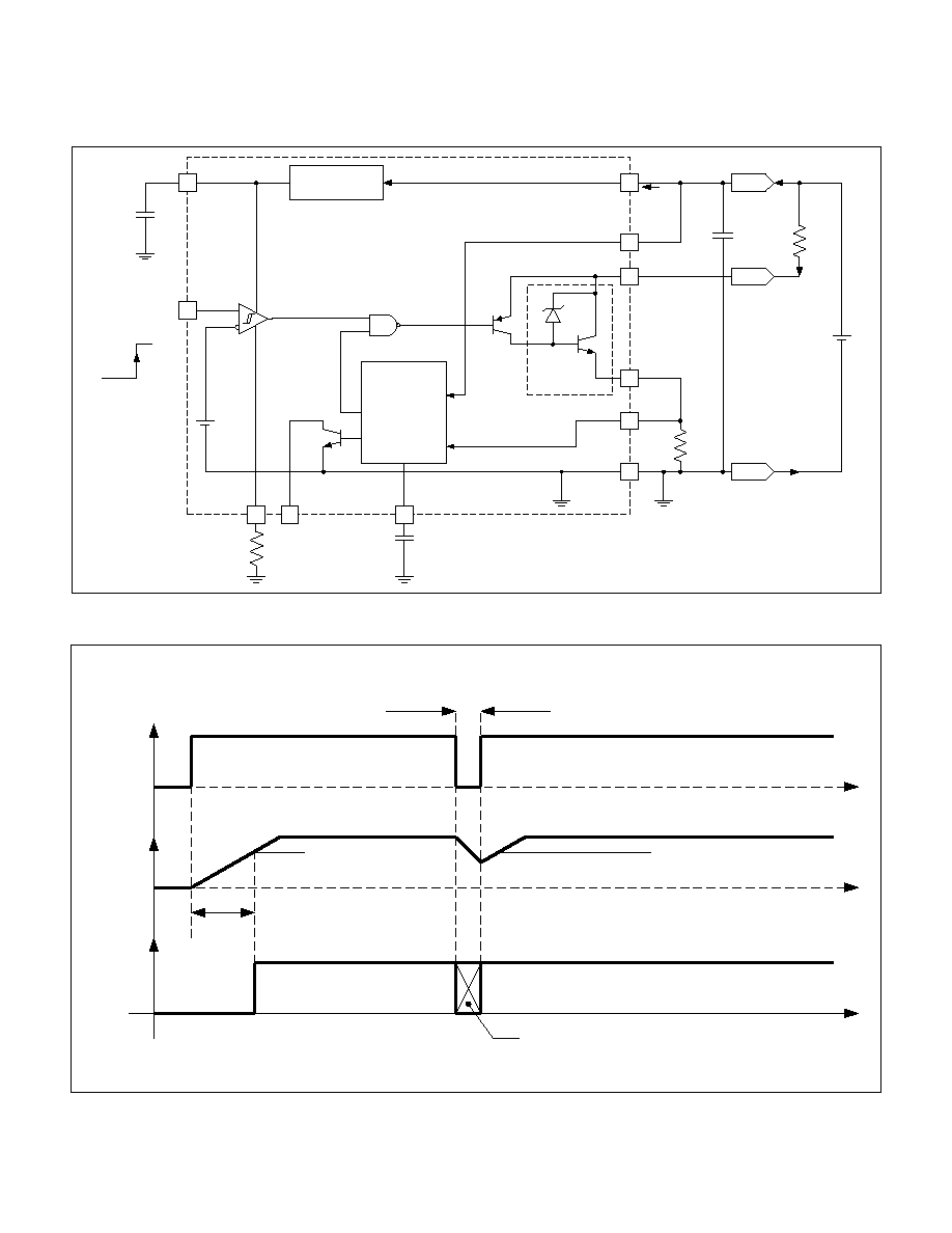
UDG-98027
8
UC17131/2/3
UC27131/2/3
UC37131/2/3
C
CDEL
13
12
11
VREF
IN
6
10
3
7
LS
CSH
2
GND
6V
PRE-REGULATOR
INPUT
COMPARATOR
1/2
VREF
HYST
9
LED
TURN-ON/OFF
AND SHORT
CIRCUIT
PROTECTION
CDEL
4
HS
5
Q
OUT
72V
≠ L
CSL
+ L
OUT
C
CC
I
GND
R
CSL
LOAD
POWER
SUPPLY
C
REF
R
HYST
VREF
GND
VCC
I
CC
Figure 2b. Low side application.
APPLICATION INFORMATION (cont.)
UDG-98028
OUTPUT
DRIVER
DISABLED
ENABLED
V
CDEL
VCC
V
FAULT_H
= 4.9V
V
FAULT_H
t
INT
ENABLED
INDETERMINATE
STATE
t
D(ON)
t
t
t
V
CDEL_MAX
= 5.8V
Figure 3a. Power interrupt ignore operation, high side configuration, V
IN
= 5VDC.
UDG-98029

9
UC17131/2/3
UC27131/2/3
UC37131/2/3
OUTPUT
DRIVER
DISABLED
ENABLED
V
CDEL
VCC
t
INT
ENABLED
INDETERMINATE
STATE
t
D(ON)
t
t
t
V
CDEL_MAX
= 5.8V
LED
V
FAULT_H
t
t
D(OFF)
V
FAULT_H
= 4.9V
DISABLED
V
FAULT_L
= 1.0V
t
D(ON)
Figure 3b. Power interrupt fault operation, high side configuration, V
IN
= 5VDC.
APPLICATION INFORMATION (cont.)
UDG-98030
OUTPUT
DRIVER
V
CDEL
I
LOAD
t
SC
t
t
t
LED
t
t
R(OFF)
4.9V
Figure 3c. Overcurrent fault operation.
UDG-98031
UNITRODE CORPORATION
7 CONTINENTAL BOULEVARD
∑
MERRIMACK, NH 03054
TEL (603) 424-2410
∑
FAX (603) 424-3460

IMPORTANT NOTICE
Texas Instruments and its subsidiaries (TI) reserve the right to make changes to their products or to discontinue
any product or service without notice, and advise customers to obtain the latest version of relevant information
to verify, before placing orders, that information being relied on is current and complete. All products are sold
subject to the terms and conditions of sale supplied at the time of order acknowledgement, including those
pertaining to warranty, patent infringement, and limitation of liability.
TI warrants performance of its semiconductor products to the specifications applicable at the time of sale in
accordance with TI's standard warranty. Testing and other quality control techniques are utilized to the extent
TI deems necessary to support this warranty. Specific testing of all parameters of each device is not necessarily
performed, except those mandated by government requirements.
CERTAIN APPLICATIONS USING SEMICONDUCTOR PRODUCTS MAY INVOLVE POTENTIAL RISKS OF
DEATH, PERSONAL INJURY, OR SEVERE PROPERTY OR ENVIRONMENTAL DAMAGE ("CRITICAL
APPLICATIONS"). TI SEMICONDUCTOR PRODUCTS ARE NOT DESIGNED, AUTHORIZED, OR
WARRANTED TO BE SUITABLE FOR USE IN LIFE-SUPPORT DEVICES OR SYSTEMS OR OTHER
CRITICAL APPLICATIONS. INCLUSION OF TI PRODUCTS IN SUCH APPLICATIONS IS UNDERSTOOD TO
BE FULLY AT THE CUSTOMER'S RISK.
In order to minimize risks associated with the customer's applications, adequate design and operating
safeguards must be provided by the customer to minimize inherent or procedural hazards.
TI assumes no liability for applications assistance or customer product design. TI does not warrant or represent
that any license, either express or implied, is granted under any patent right, copyright, mask work right, or other
intellectual property right of TI covering or relating to any combination, machine, or process in which such
semiconductor products or services might be or are used. TI's publication of information regarding any third
party's products or services does not constitute TI's approval, warranty or endorsement thereof.
Copyright
©
1999, Texas Instruments Incorporated