 | –≠–ª–µ–∫—Ç—Ä–æ–Ω–Ω—ã–π –∫–æ–º–ø–æ–Ω–µ–Ω—Ç: UC2715DTR | –°–∫–∞—á–∞—Ç—å:  PDF PDF  ZIP ZIP |
UC1714/5
UC2714/5
UC3714/5
FEATURES
∑ Single Input (PWM and TTL
Compatible)
∑ High Current Power FET Driver, 1.0A
Source/2A Sink
∑ Auxiliary Output FET Driver, 0.5A
Source/1A Sink
∑ Time Delays Between Power and
Auxiliary Outputs Independently
Programmable from 50ns to 500ns
∑ Time Delay or True Zero-Voltage
Operation Independently Configurable
for Each Output
∑ Switching Frequency to 1MHz
∑ Typical 50ns Propagation Delays
∑ ENBL Pin Activates 220µA Sleep
Mode
∑ Power Output is Active Low in Sleep
Mode
∑ Synchronous Rectifier Driver
DESCRIPTION
These two families of high speed drivers are designed to provide drive
waveforms for complementary switches. Complementary switch configura-
tions are commonly used in synchronous rectification circuits and active
clamp/reset circuits, which can provide zero voltage switching. In order to
facilitate the soft switching transitions, independently programmable delays
between the two output waveforms are provided on these drivers. The de-
lay pins also have true zero voltage sensing capability which allows imme-
diate activation of the corresponding switch when zero voltage is applied.
These devices require a PWM-type input to operate and can be interfaced
with commonly available PWM controllers.
In the UC1714 series, the AUX output is inverted to allow driving a
p-channel MOSFET. In the UC1715 series, the two outputs are configured
in a true complementary fashion.
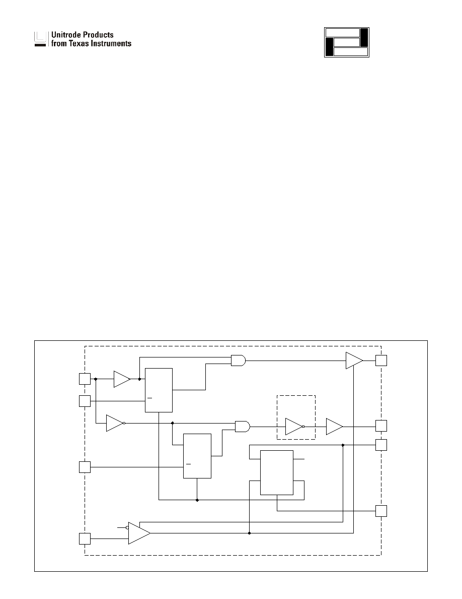
6
5
7
8
INPUT
T1
T2
ENBL
S
Q
R
TIMER
V
REF
S
Q
R
TIMER
V
REF
50ns ≠500ns
50ns ≠500ns
5V
ENBL
V
CC
3V
GND
BIAS
1.4V
ENABLE
UC1714
ONLY
4
AUX
2
PWR
1
VCC
LOGIC
GATES
TIMER
REF
3
GND
BLOCK DIAGRAM
Complementary Switch FET Drivers
SLUS170A - FEBRUARY 1999 - REVISED JANUARY 2002
UDG-99028
Note: Pin numbers refer to J, N and D packages.
application
INFO
available
2
UC1714/5
UC2714/5
UC3714/5
ABSOLUTE MAXIMUM RATINGS
Supply Voltage V
CC
. . . . . . . . . . . . . . . . . . . . . . . . . . . . . . . 20V
Power Driver IOH
continuous . . . . . . . . . . . . . . . . . . . . . . . . . . . . . . . .
-200mA
peak . . . . . . . . . . . . . . . . . . . . . . . . . . . . . . . . . . . . . . . . .
-1A
Power Driver IOL
continuous . . . . . . . . . . . . . . . . . . . . . . . . . . . . . . . . . 400mA
peak. . . . . . . . . . . . . . . . . . . . . . . . . . . . . . . . . . . . . . . . . . 2A
Auxiliary Driver IOH
continuous . . . . . . . . . . . . . . . . . . . . . . . . . . . . . . . .
-100mA
peak . . . . . . . . . . . . . . . . . . . . . . . . . . . . . . . . . . . . .
-500mA
Auxiliary Driver IOL
continuous . . . . . . . . . . . . . . . . . . . . . . . . . . . . . . . . . 200mA
peak. . . . . . . . . . . . . . . . . . . . . . . . . . . . . . . . . . . . . . . . . . 1A
Input Voltage Range (INPUT, ENBL) . . . . . . . . . .
-0.3V to 20V
Storage Temperature Range . . . . . . . . . . . . . .
-65∞C to 150∞C
Operating Junction Temperature (Note 1) . . . . . . . . . . . . 150
∞C
Lead Temperature (Soldering 10 seconds) . . . . . . . . . . . 300
∞C
Note 1: Unless otherwise indicated, voltages are referenced to
ground and currents are positive into, negative out of, the speci-
fied terminals.
Note 2: Consult Packaging Section of databook for thermal limi-
tations and specifications of packages.
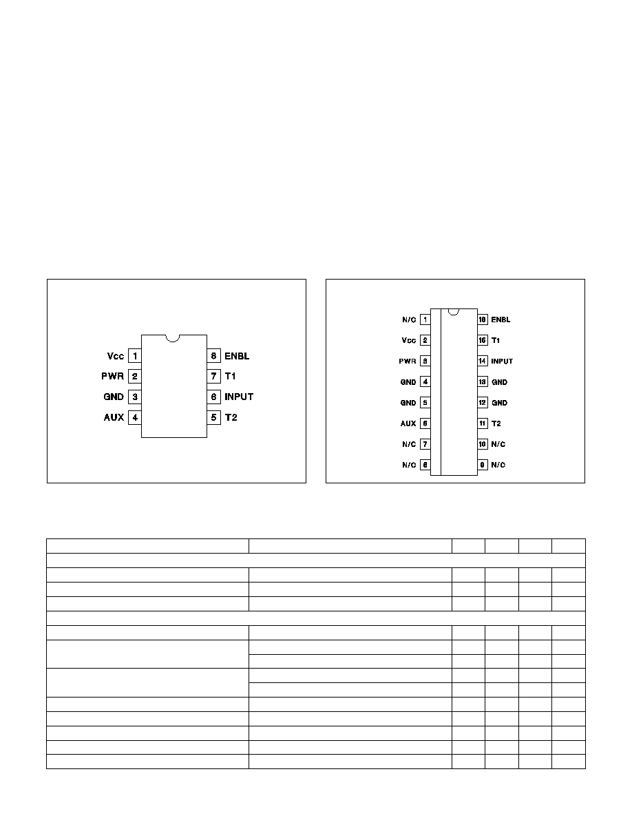
CONNECTION DIAGRAMS
DIL-8, SOIC-8 (Top View)
J or N, D Packages
ELECTRICAL CHARACTERISTICS:
Unless otherwise stated, V
CC
= 15V, ENBL
2V, R
T
1 = 100k
from T1 to GND,
R
T
2 = 100k
from T2 to GND, and -55∞C < T
A
< 125∞C for the UC1714/5,
-40∞C < T
A
< 85∞C for the UC2714/5, and 0
∞C < T
A
<
70
∞C for the UC3714/5, T
A
= T
J
.
PARAMETER
TEST CONDITIONS
MIN
TYP
MAX
UNITS
Overall
V
CC
7
20
V
I
CC
, nominal
ENBL = 2.0V
18
24
mA
I
CC
, sleep mode
ENBL = 0.8V
200
300
µA
Power Driver (PWR)
Pre Turn-on PWR Output, Low
V
CC
= 0V, I
OUT
= 10mA, ENBL
0.8V
0.3
1.6
V
PWR Output Low, Sat. (V
PWR
)
INPUT = 0.8V, I
OUT
= 40mA
0.3
0.8
V
INPUT = 0.8V, I
OUT
= 400mA
2.1
2.8
V
PWR Output High, Sat. (V
CC -
V
PWR
)
INPUT = 2.0V, I
OUT
=
-20mA
2.1
3
V
INPUT = 2.0V, I
OUT
=
-200mA
2.3
3
V
Rise Time
C
L
= 2200pF
30
60
ns
Fall Time
C
L
= 2200pF
25
60
ns
T1 Delay, AUX to PWR
INPUT rising edge, R
T
1 = 10k
(Note 4)
20
35
80
ns
T1 Delay, AUX to PWR
INPUT rising edge, R
T
1 = 100k
(Note 4)
350
500
700
ns
PWR Prop Delay
INPUT falling edge, 50% (Note 3)
35
100
ns
SOIC-16 (Top View)
DP Package
3
UC1714/5
UC2714/5
UC3714/5
ELECTRICAL CHARACTERISTICS:
Unless otherwise stated, V
CC
= 15V, ENBL
2V, R
T
1 = 100k
from T1 to GND,
R
T
2 = 100k
from T2 to GND, and -55∞C < T
A
< 125∞C for the UC1714/5,
-40∞C < T
A
< 85∞C for the UC2714/5, and 0
∞C < T
A
<
70
∞C for the UC3714/5, T
A
= T
J
.
PARAMETER
TEST CONDITIONS
MIN
TYP
MAX
UNITS
Auxiliary Driver (AUX)
AUX Output Low, Sat (V
AUX)
V
IN
= 2.0V, I
OUT
= 20mA
0.3
0.8
V
V
IN
= 2.0V, I
OUT
= 200mA
1.8
2.6
V
AUX Output High, Sat (V
CC
≠ V
AUX
)
V
IN
= 0.8V, I
OUT
= -10mA
2.1
3.0
V
V
IN
= 0.8V, I
OUT
= -100mA
2.3
3.0
V
Rise Time
C
L
= 1000pF
45
60
ns
Fall Time
C
L
= 1000pF
30
60
ns
T2 Delay, PWR to AUX
INPUT falling edge, R
T
2 = 10k
(Note 4)
20
50
80
ns
T2 Delay, PWR to AUX
INPUT falling edge, R
T
2 = 100k
(Note 4)
250
350
550
ns
AUX Prop Delay
INPUT rising edge, 50% (Note 3)
35
80
ns
Enable (ENBL)
Input Threshold
0.8
1.2
2.0
V
Input Current, I
IH
ENBL = 15V
1
10
µA
Input Current, I
IL
ENBL = 0V
-1
-10
µA
T1
Current Limit
T1 = 0V
-1.6
-2
mA
Nominal Voltage at T1
2.7
3
3.3
V
Minimum T1 Delay
T1 = 2.5V, (Note 4)
40
70
ns
T2
Current Limit
T2 = 0V
-1.2
-2
mA
Nominal Voltage at T2
2.7
3
3.3
V
Minumum T2 Delay
T2 = 2.5V, (Note 4)
50
100
ns
Input (INPUT)
Input Threshold
0.8
1.4
2.0
V
Input Current, I
IH
INPUT = 15V
1
10
µ
A
Input Current, I
IL
INPUT = 0V
-
5
-20
µA
Note 3: Propagation delay times are measured from the 50% point of the input signal to the 10% point of the output signal's transi-
tion with no load on outputs.
Note 4: T1 delay is defined from the 50% point of the transition edge of AUX to the 10% of the rising edge of PWR. T2 delay is de-
fined from the 90% of the falling edge of PWR to the 50% point of the transition edge of AUX.
PIN DESCRIPTIONS
AUX: The AUX switches immediately at INPUT's rising
edge but waits through the T2 delay after INPUT's falling
edge before switching. AUX is capable of sourcing 0.5A
and sinking 1.0A of drive current. See the Time Relation-
ships diagram below for the difference between the
UC1714 and UC1715 for INPUT, MAIN, and AUX. During
sleep mode, AUX is inactive with a high impedance.
ENBL: The ENBL input switches at TTL logic levels (ap-
proximately 1.2V), and its input range is from 0V to 20V.
The ENBL input will place the device into sleep mode
when it is a logical low. The current into V
CC
during the
sleep mode is typically 220
µA.
GND: This is the reference pin for all input voltages and
the return point for all device currents. It carries the full
peak sinking current from the outputs. Any tendency for
the outputs to ring below GND voltage must be damped
or clamped such that GND remains the most negative
potential.
4
UC1714/5
UC2714/5
UC3714/5
INPUT: The input switches at TTL logic levels (approxi-
mately 1.4V) but the allowable range is from 0V to 20V,
allowing direct connection to most common IC PWM con-
troller outputs. The rising edge immediately switches the
AUX output, and initiates a timing delay, T1, before
switching on the PWR output. Similarly, the INPUT falling
edge immediately turns off the PWR output and initiates
a timing delay, T2, before switching the AUX output.
It should be noted that if the input signal comes from a
controller with FET drive capability, this signal provides
another option. INPUT and PWR provide a delay only at
the leading edge while INPUT and AUX provide the delay
at the trailing edge.
PWR: The PWR output waits for the T1 delay after the
INPUT's rising edge before switching on, but switches off
immediately at INPUT's falling edge (neglecting propaga-
tion delays). This output is capable of sourcing 1A and
sinking 2A of peak gate drive current. PWR output in-
cludes a passive, self-biased circuit which holds this pin
active low, when ENBL
0.8V regardless of VCC's volt-
age.
T1: A resistor to ground programs the time delay be-
tween AUX switch turn-off and PWR turn-on.
T2: This pin functions in the same way as T1 but controls
the time delay between PWR turn-off and activation of
the AUX switch.
T1, T2: The resistor on each of these pins sets the
charging current on internal timing capacitors to provide
independent time control. The nominal voltage level at
each pin is 3V and the current is internally limited to
1mA. The total delay from INPUT to each output includes
a propagation delay in addition to the programmable
timer but since the propagation delays are approximately
equal, the relative time delay between the two outputs
can be assumed to be solely a function of the pro-
grammed delays. The relationship of the time delay vs.
RT is shown in the Typical Characteristics curves.
Either or both pins can alternatively be used for voltage
sensing in lieu of delay programming. This is done by
pulling the timer pins below their nominal voltage level
which immediately activates the timer output.
VCC: The V
CC
input range is from 7V to 20V. This pin
should be bypassed with a capacitor to GND consistent
with peak load current demands.
PIN DESCRIPTIONS (cont.)
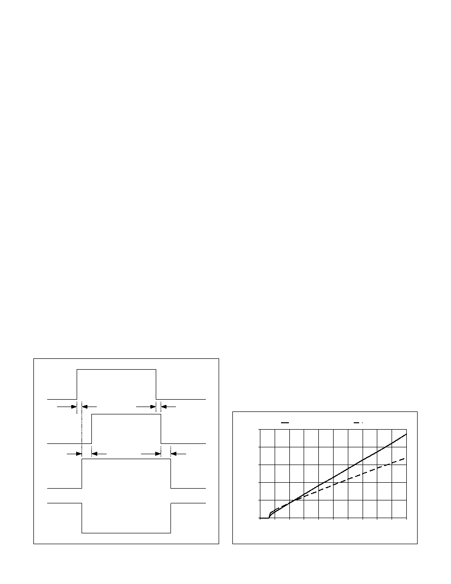
PROPAGATION
DELAYS
INPUT
PWR OUTPUT
T1 DELAY
T2 DELAY
UC1714 AUX OUTPUT
UC1715 AUX OUTPUT
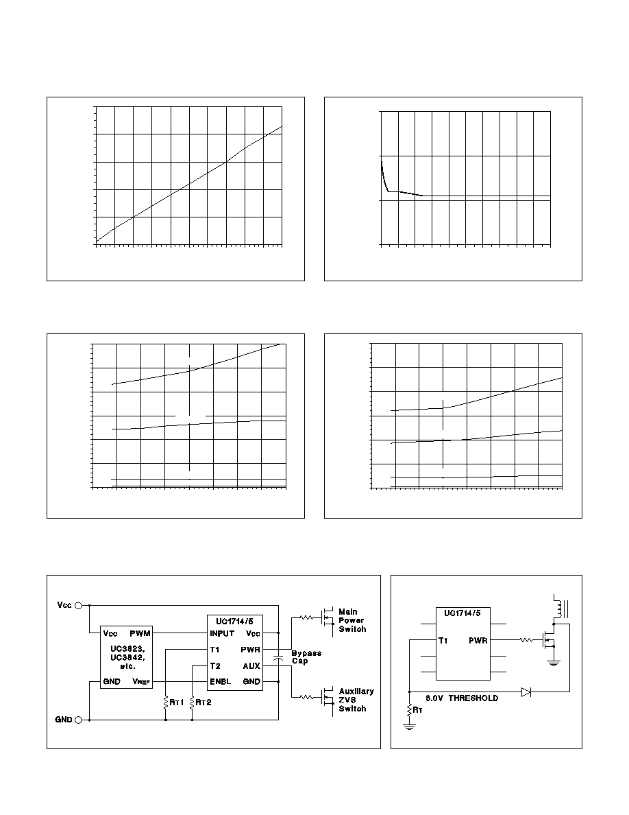
TYPICAL CHARACTERISTICS
Time relationships. (Notes 3, 4)
UDG-99027
0
100
200
300
400
500
0
10
20
30
40
50
60
70
80
90
100
RT (kW)
DELA
Y
(
ns)
T1 vs RT1
T2 vs RT2
T1 Delay, T2 Delay vs. R
T
5
UC1714/5
UC2714/5
UC3714/5
15
16
17
18
0
10
20
30
40
50
60
70
80
90
100
R
T
(k
)
Icc
(mA)
I
CC
vs R
T
with Opposite R
T
= 50k
0
100
200
300
400
500
600
-75
-50
-25
0
25
50
75
100
125
Temperature (∞C)
De
ad
ba
nd
De
lay
(n
s)
RT1 = 100k
RT1 = 50k
RT1 = 10k
RT1 < 6k
T1 Deadband vs. Temperature AUX to PWR
Figure 1. Typical application with timed delays.
TYPICAL APPLICATIONS
UDG-94011
Figure 2. Using the timer input for
zero-voltage sensing.
UDG-94012
0
100
200
300
400
500
600
-75
-50
-25
0
25
50
75
100
125
Temperature (∞C)
De
ad
ba
nd
De
lay
(n
s)
RT2 = 100k
RT2 = 50k
RT2 = 10k
RT2 < 6k
T2 Deadband vs. Temperature PWR to AUX
16
17
18
19
20
21
0
100 200 300 400 500 600 700 800 900 1000
Switching Frequency (kHz)
Icc (mA)
TYPICAL CHARACTERISTICS (cont.)
I
CC
vs Switching Frequency with No Load and 50%
Duty Cycle R
T
1 = R
T
2 = 50k

6
UC1714/5
UC2714/5
UC3714/5
Figure 5. Synchronous rectifier application with a charge pump to drive the high-side n-channel buck switch.
V
IN
is limited to 10V as V
CC
will rise to approximately 2V
IN
.
UDG-94014-1
Figure 4. Using the UC1715 as a complementary synchronous rectifier switch driver with n-channel FETs
UDG-94015-2
Figure 3. Self-actuated sleep mode with the absence of an input PWM signal. Wake up occurs with the first
pulse while turn-off is determined by the (RTO
CTO) time constant.
TYPICAL APPLICATIONS (cont.)
UDG-94013
7
UC1714/5
UC2714/5
UC3714/5
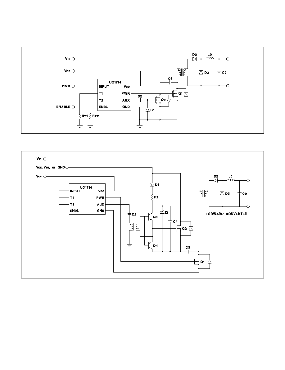
Figure 7. Using an N-channel active reset switch with a floating drive command.
UDG-94017-1
Figure 6. Typical forward converter topology with active reset provided by the UC1714 driving an N-channel
switch (Q1) and a P-channel auxilliary switch (Q2).
TYPICAL APPLICATIONS (cont.)
UDG-94016-1

IMPORTANT NOTICE
Texas Instruments Incorporated and its subsidiaries (TI) reserve the right to make corrections, modifications,
enhancements, improvements, and other changes to its products and services at any time and to discontinue
any product or service without notice. Customers should obtain the latest relevant information before placing
orders and should verify that such information is current and complete. All products are sold subject to TI's terms
and conditions of sale supplied at the time of order acknowledgment.
TI warrants performance of its hardware products to the specifications applicable at the time of sale in
accordance with TI's standard warranty. Testing and other quality control techniques are used to the extent TI
deems necessary to support this warranty. Except where mandated by government requirements, testing of all
parameters of each product is not necessarily performed.
TI assumes no liability for applications assistance or customer product design. Customers are responsible for
their products and applications using TI components. To minimize the risks associated with customer products
and applications, customers should provide adequate design and operating safeguards.
TI does not warrant or represent that any license, either express or implied, is granted under any TI patent right,
copyright, mask work right, or other TI intellectual property right relating to any combination, machine, or process
in which TI products or services are used. Information published by TI regarding third≠party products or services
does not constitute a license from TI to use such products or services or a warranty or endorsement thereof.
Use of such information may require a license from a third party under the patents or other intellectual property
of the third party, or a license from TI under the patents or other intellectual property of TI.
Reproduction of information in TI data books or data sheets is permissible only if reproduction is without
alteration and is accompanied by all associated warranties, conditions, limitations, and notices. Reproduction
of this information with alteration is an unfair and deceptive business practice. TI is not responsible or liable for
such altered documentation.
Resale of TI products or services with statements different from or beyond the parameters stated by TI for that
product or service voids all express and any implied warranties for the associated TI product or service and
is an unfair and deceptive business practice. TI is not responsible or liable for any such statements.
Mailing Address:
Texas Instruments
Post Office Box 655303
Dallas, Texas 75265
Copyright
2002, Texas Instruments Incorporated