 | –≠–ª–µ–∫—Ç—Ä–æ–Ω–Ω—ã–π –∫–æ–º–ø–æ–Ω–µ–Ω—Ç: UC2717J | –°–∫–∞—á–∞—Ç—å:  PDF PDF  ZIP ZIP |
7/95
∑
Half-step and Full-step Capability
∑
Bipolar Constant Current Motor Drive
∑
Built-in Fast Recovery Schottky
Commutating Diodes
∑
Wide Range of Current Control 5-1000mA
∑
Wide Voltage Range 10-45V
∑
Designed for Unregulated Motor Supply
Voltage
∑
Current Levels can be Selected in Steps
or Varied Continuously
∑
Thermal Overload Protection
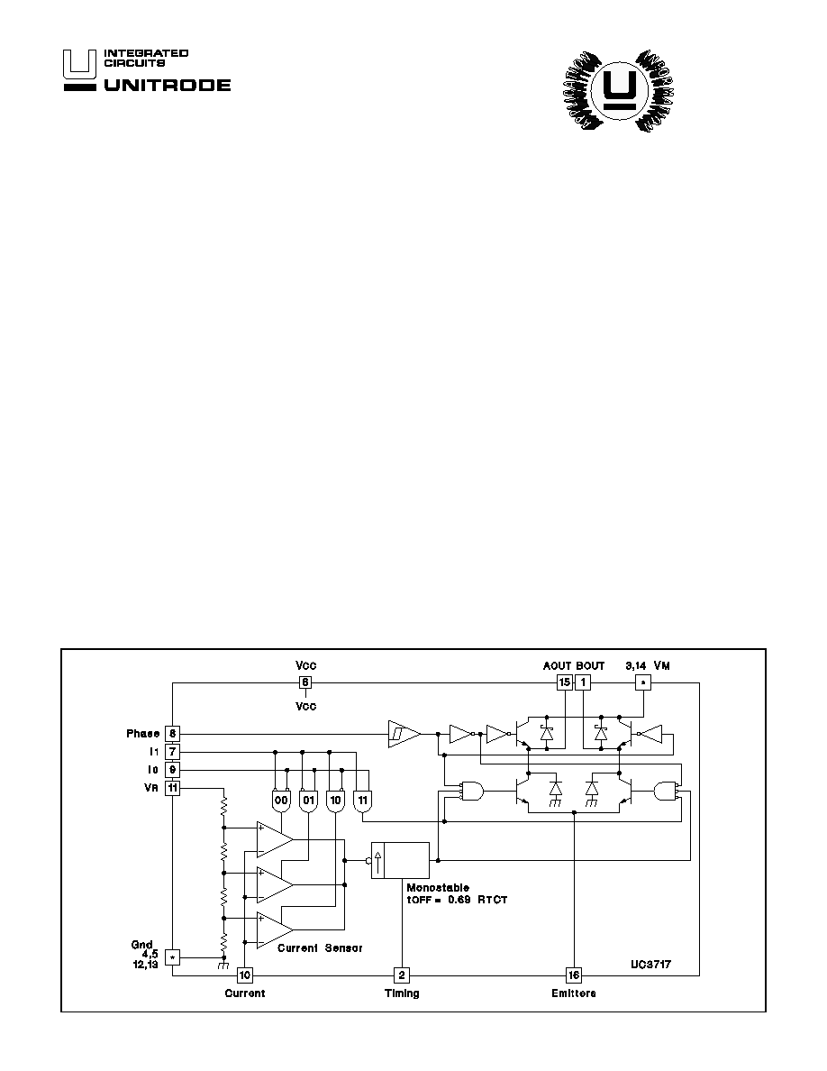
Stepper Motor Drive Circuit
The UC3717 has been designed to control and drive the current in
one winding of a bipolar stepper motor. The circuit consists of an LS-
TTL-compatible logic input, a current sensor, a monostable and an
output stage with built-in protection diodes. Two UC3717s and a few
external components form a complete control and drive unit for LS-
TTL or micro-processor controlled stepper motor systems.
The UC1717 is characterized for operation over the full military tem-
perature range of -55∞C to +125∞C, the UC2717 is characterized for
-25∞C to +85∞C, and the UC3717 is characterized for 0∞C to +70∞C.
UC1717
UC2717
UC3717
BLOCK DIAGRAM
FEATURES
DESCRIPTION
Voltage
Logic Supply, V
CC
. . . . . . . . . . . . . . . . . . . . . . . . . . . . . . . . . . . . . . . 7V
Output Supply, V
M
. . . . . . . . . . . . . . . . . . . . . . . . . . . . . . . . . . . . . . 45V
Input Voltage
Logic Inputs (Pins 7, 8, 9). . . . . . . . . . . . . . . . . . . . . . . . . . . . . . . . . . 6V
Analog Input (Pin 10) . . . . . . . . . . . . . . . . . . . . . . . . . . . . . . . . . . . . Vcc
Reference Input (Pin 11) . . . . . . . . . . . . . . . . . . . . . . . . . . . . . . . . . 15V
Input Current
Logic Inputs (Pins 7, 8, 9) . . . . . . . . . . . . . . . . . . . . . . . . . . . . . . . -10mA
Analog Inputs (Pins 10, 11) . . . . . . . . . . . . . . . . . . . . . . . . . . . . . . -10mA
Output Current (Pins 1, 15) . . . . . . . . . . . . . . . . . . . . . . . . . . . . . . . .
±
1A
Junction Temperature, T
J
. . . . . . . . . . . . . . . . . . . . . . . . . . . . . . . +150∞C
Storage Temperature Range, T
S
. . . . . . . . . . . . . . . . . . -55∞C to +150∞C
ABSOLUTE MAXIMUM RATINGS (Note 1)
Note 1: All voltages are with respect to ground, Pins
4,5, 12, 13. Pin numbers refer to DIL-16 package. Cur-
rents are positive into, negative out of the specified ter-
minal.
Note 2: Consult Packaging Section of Databook for in-
formation on thermal limitations and considerations of
package.
UC1717
UC2717
UC3717
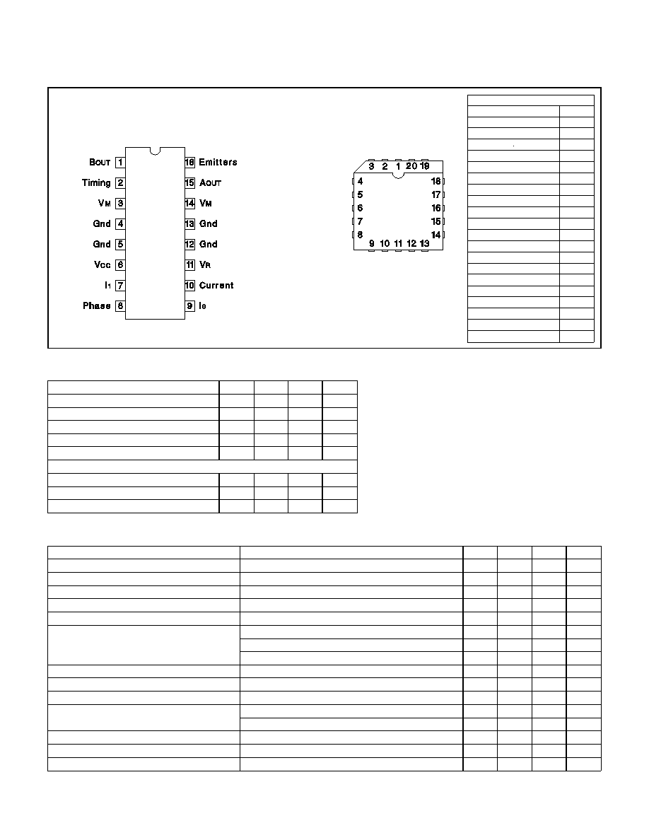
PACKAGE PIN FUNCTION
FUNCTION
PIN
N/C
1
B
OUT
2
Timing
3
V
M
4
Gnd
5
N/C
6
Gnd
7
V
CC
8
I
1
9
Phase
10
N/C
11
I
0
12
Current
13
V
R
14
Gnd
15
N/C
16
Gnd
17
V
m
18
A
OUT
19
Emitters
20
DIL-16 (TOP VIEW)
J or N Package
CONNECTION DIAGRAMS
ELECTRICAL CHARACTERISTICS
Unless otherwise specified, these specifications apply for V
CC
= 5V, T
A
= T
J
.
PARAMETER
MIN
TYP
MAX
UNITS
Supply Voltage, V
CC
4.75
5
5.25
V
Supply Voltage, V
M
10
40
V
Output Current. I
M
20
800
mA
Rise Time Logic Inputs, t
R
2
µ
s
Fall Time Logic Inputs, t
F
2
µ
s
Ambient Temperature, T
A
UC1717
-55
125
∞C
UC2717
-25
85
∞C
UC3717
0
70
∞C
RECOMMENDED OPERATING CONDITIONS
PARAMETER
TEST CONDITIONS
MIN
TYP
MAX
UNITS
Supply Current, I
CC
25
mA
High-Level Input Voltage, Pins 7, 8, 9
2.0
V
Low-Level Input Voltage, Pins 7, 8, 9
0.8
V
High-Level Input Current, Pins 7, 8, 9
V
I
= 2.4V
20
µ
A
Low Level Input Current, Pins 7, 8, 9
V
I
= 0.4V
-0.4
mA
Comparator Threshold Voltage
I
O
= 0, I
1
= 0, V
R
= 5.0V
390
420
440
mV
I
O
= 1, I
1
= 0, V
R
= 5.0V
230
250
270
mV
I
O
= 0, I
1
= 1, V
R
= 5.0V
65
80
90
mV
Comparator Input Current
-20
20
µ
A
Output Leakage Current
I
O
= 1, I
1
= 1, T
A
= +25∞C
100
µ
A
Total Saturation Voltage Drop
I
M
= 500mA
4.0
V
Total Power Dissipation
I
M
= 500mA, f
S
= 30kHz
1.4
2.1
W
I
M
= 800mA, f
S
= 30kHz
2.9
3.1
W
Cut Off Time, t
OFF
V
M
= 10V, t
ON
5
µ
s (See Figure 5 and 6)
25
30
35
µ
s
Turn Off Delay, t
D
T
A
= +25∞C; dVc/dt
50mV/
µ
s (See Figure 5 and 6)
1.6
2.0
µ
s
Thermal Shutdown Junction Temperature
+160
+180
∞C
PLCC-20 (TOP VIEW)
Q Package
2
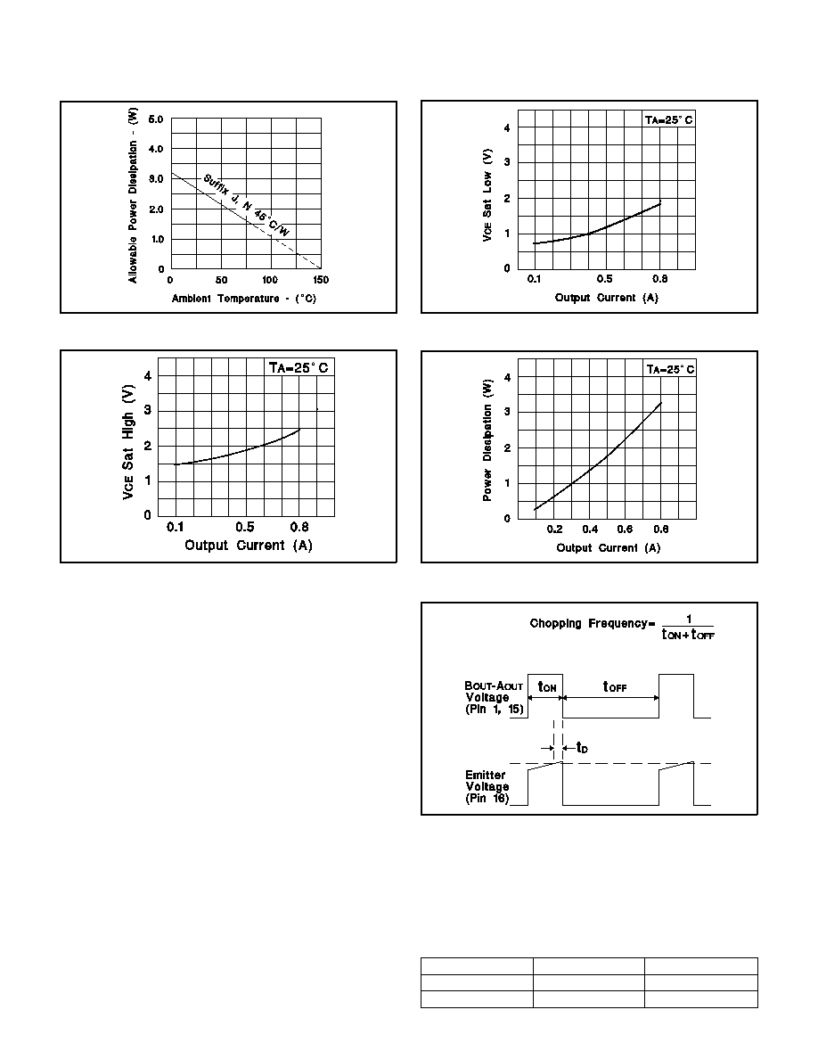
Figure 1
Figure 3:
Typical Sink Saturation Voltage vs Output Current
Figure 2:
Typical Source Saturation Voltage vs Output Current
Figure 4:
Typical Power Losses vs Output Current
UC1717
UC2717
UC3717
Figure 5:
Connections and Component Values as in Figure 6.
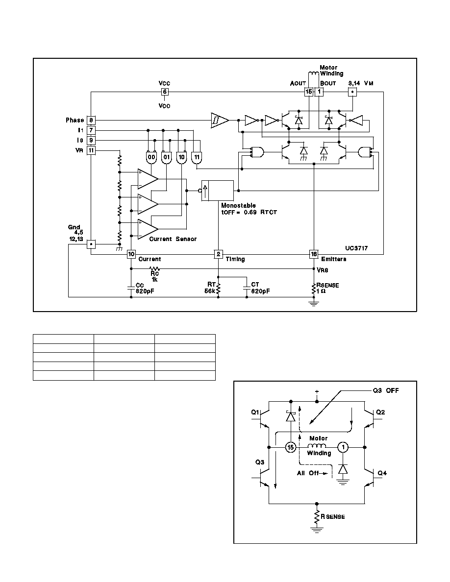
The UC3717 drive circuit shown in the block diagram in-
cludes the following functions:
(1) Phase Logic and H-Bridge Output Stage
(2) Voltage Divider with three Comparators for current control
(3) Two Logic inputs for Digital current level select
(4) Monostable for off time generation
Input Logic: If any of the logic inputs are left open, the
circuit will treat it as a high level input.
Phase Input: The phase input terminal, pin 18, controls
the direction of the current through the motor winding.
The Schmidt-Trigger input coupled with a fixed time de-
lay assures noise immunity and eliminates cross conduc-
tion in the output stage during phase changes. A low
level on the phase input will turn Q2 on and enable Q3
while a high level will turn Q1 on and enable Q4. (See
Figure 7).
Output Stage: The output stage consists of four Dar-
lington transistors and associated diodes connected in
an H-Bridge configuration. The diodes are needed to pro-
vide a current path when the transistors are being
switched. For fast recovery, Schottky diodes are used
FUNCTIONAL DESCRIPTION
across the source transistors. The Schottky diodes allow
the current to circulate through the winding while the sink
transistors are being switched off. The diodes across the
sink transistors in conjunction with the Schottkys provide
the path for the decaying current during phase reversal.
(See Figure 7).
PHASE INPUT
Q1, Q4
Q2, Q3
Low
Off
On
High
On
Off
3
I
0
I
1
CURRENT LEVEL
0
0
100%
1
0
60%
0
1
19%
1
1
Current Inhibit
Current Control: The voltage divider, comparators and
monostable provide a means for current sensing and
control. The two bit input (I
0
, I
1
) logic selects the desired
comparator. The monostable controls the off time and
therefore the magnitude of the current decrease. The
time duration is determined by R
T
and C
T
connected to
the timing terminal (pin 2). The reference terminal (pin
11) provides a means of continuously varying the cur-
rent for situations requiring half-stepping and micro-
stepping. The relationship between the logic input
signals at pin 7 and 9 in reference to the current level is
shown in Table 1. The values of the different current lev-
els are determined by the reference voltage together
with the value of the external sense resistor R
S
(pin 16).
Single-Pulse Generator: The pulse generator is a
monostable triggered on the positive going edge of the
comparator. Its output is high during the pulse time and
this pulse switches off the power feed to the motor wind-
ing causing the current to decay. The time is determined
by the external timing components R
T
and C
T
as:
T
OFF
= 0.69 R
T
C
T
If a new trigger signal should occur during T
OFF
, it is ig-
nored.
Figure 6
Figure 7:
Simplified Schematic of Output Stage
UC1717
UC2717
UC3717
Note: Dashed lines indicate current decay paths.
4
Overload Protection: The circuit is equipped with a
thermal shutdown function, which will limit the junction
temperature by reducing the output current. It should be
noted however, that a short circuit of the output is not
permitted.
Operation: When the voltage is applied across the motor
winding the current rises linearly and appears across the
external sense resistor as an analog voltage. This volt-
age is fed through a low pass filter R
C
, C
C
to the voltage
comparator (pin 10). At the moment the voltage rises be-
yond the comparator threshold voltage the monostable is
triggered and its output turns off the sink transistors. The
current then circulates through the source transistor and
the appropriate Schottky diode. After the one shot has
timed out, the sink transistsor is turned on again and the
procedure repeated until a current reverse command is
given. By reversing the logic level of the phase input (pin
8), both active transistors are being turned off and the
opposite pair turned on. When this happens the current
must first decay to zero before it can reverse. The cur-
rent path then provided is through the two diodes and the
power-supply. Refer to Figure 7. It should be noted at
this time that the slope of the current decay is steeper,
and this is due to the higher voltage build up across the
winding. For better speed performance of the stepping
motor at half step mode, the phase logic level should be
changed at the same time the current inhibit is applied. A
typical current wave form is shown in Figure 8.
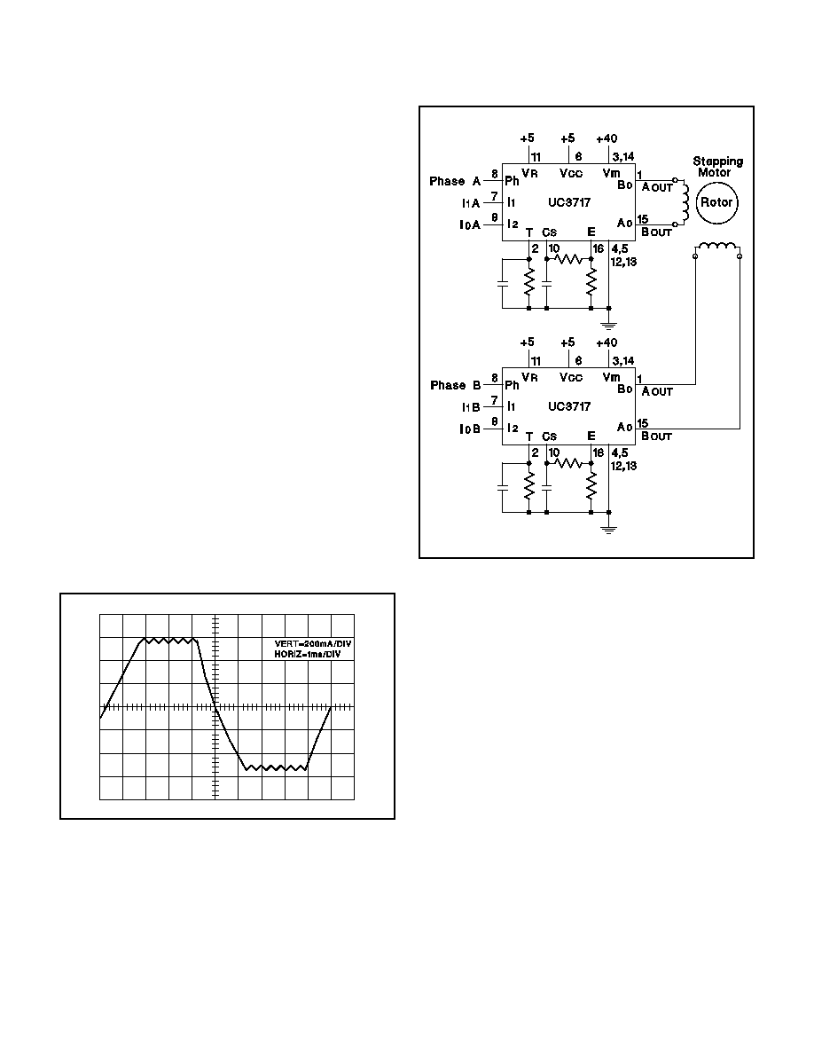
APPLICATIONS
A typical chopper drive for a two phase bipolar perma-
nent magnet or hybrid stepping motor is shown in Figure
9. The input can be controlled by a microprocessor, TTL,
LS or CMOS logic.
The timing diagram in Figure 10 shows the required sig-
nal input for a two phase, full step, stepping sequence.
Figure 11 shows a one phase, full step, stepping se-
quence, commonly referred to as wave drive. Figure 12
shows the required input signal for a one phase-two
phase stepping sequence called half-stepping.
The circuit of Figure 13 provides the signal shown in Fig-
ure 10, and in conjunction with the circuit shown in Fig-
ure 9, will implement a pulse-to-step two phase, full step,
bidirectional motor drive.
The schematic of Figure 14 shows a pulse to half step
circuit generating the signal shown in Figure 12. Care
has been taken to change the phase signal the same
time the current inhibit is applied. This will allow the cur-
rent to decay faster and therefore enhance the motor
performance at higher step rates.
Using the UC3717 to drive the L298 provides a uniquely
packaged state-of-the-art high power stepper motor con-
trol and drive. See Figure 15.
Figure 8
FUNCTIONAL DESCRIPTION (cont.)
Figure 9
UC1717
UC2717
UC3717
5