 | –≠–ª–µ–∫—Ç—Ä–æ–Ω–Ω—ã–π –∫–æ–º–ø–æ–Ω–µ–Ω—Ç: UC28023DW | –°–∫–∞—á–∞—Ç—å:  PDF PDF  ZIP ZIP |
UC28023
UC28025
SLUS557B - MARCH 2003 - REVISED APRIL 2004
ECONOMY HIGH SPEED PWM CONTROLLER
1
www.ti.com
FEATURES
D
Peak Current Mode, Average Current Mode,
or Voltage Mode (with Feed-Forward) Control
Methods
D
Practical Operation Up to 1 MHz
D
50-ns Propagation Delay to Output
D
±
1.5-A Peak Totem Pole Outputs
D
9-V to 30-V Nominal Operational Voltage
Range
D
Wide Bandwidth Error Amplifier
D
Fully Latched Logic with Double Pulse
Suppression
D
Pulse-by-Pulse Current Limiting
D
Programmable Maximum Duty Cycle Control
D
Under-Voltage Lockout with Hysteresis
D
Trimmed 5.1-V Reference with UVLO
D
Same Functionality as UC3823 and UC3825
APPLICATIONS
D
Off-Line and DC/DC Power Supplies
D
Converters Using Voltage Mode, Peak
Current Mode, or Average Current Mode
Control Methods
D
Single-Ended or Two-Switch Topology
Designs
DESCRIPTION
The UC28023 and UC28025 are fixed-frequency
PWM controllers optimized for high-frequency
switched-mode power supply applications. The
UC28023 is a single output PWM for single-ended
topologies while the UC28025 offers dual
alternating outputs for double-ended and full
bridge topologies.
Targeted for cost effective solutions with minimal
external components, UC2802x include an
oscillator, a temperature compensated reference,
a wide band width error amplifier, a high-speed
current-sense comparator and high-current
active-high totem-pole outputs to directly drive
external MOSFETs.
Protection circuitry includes a current limit
comparator with a 1-V threshold, a TTL
compatible shutdown port, and a soft-start pin
which will double as a maximum duty cycle clamp.
The logic is fully latched to provide jitter free
operation and prohibit multiple pulses at an
output. An undervoltage lockout section with
800
mV of hysteresis assures low start-up
current. During undervoltage lockout, the outputs
are high impedance. Particular care was given to
minimizing propagation delays through the
comparators and logic circuitry while maximizing
bandwidth and slew rate of the error amplifier.
Devices are available in the industrial temperature
range of -40
∞
C to 105
∞
C. Package offerings are
16-pin SOICW (DW), or 16-pin PDIP (N)
packages.
ORDERING INFORMATION
TA = TJ
OUTPUT
EXTERNAL CURRENT
PACKAGED DEVICES
TA = TJ
OUTPUT
CONFIGURATION
EXTERNAL CURRENT
LIMIT REFERENCE
PDIP-16 (N)
SOICW-16 (DW)
- 40
∞
C to 105
∞
C
Single
Yes
UC28023N
UC28023DW
- 40
∞
C to 105
∞
C
Dual Alternating
No
UC28025N
UC28025DW
(1) The DW package are also available taped and reeled. Add an R suffix to the device type (i.e., UC28023DWR (2,000 devices per reel).
PRODUCTION DATA information is current as of publication date.
Products conform to specifications per the terms of Texas Instruments
standard warranty. Production processing does not necessarily include
testing of all parameters.
Copyright
2004, Texas Instruments Incorporated

UC28023
UC28025
SLUS557B - MARCH 2003 - REVISED APRIL 2004
2
www.ti.com
These devices have limited built-in ESD protection. The leads should be shorted together or the device placed in conductive foam
during storage or handling to prevent electrostatic damage to the MOS gates.
ABSOLUTE MAXIMUM RATINGS
over operating free-air temperature range unless otherwise noted(1)
UC28023
UC28025
RATING
UNIT
Input voltage range,
VC, VCC
VC, VCC
30
V
Output current, IOUT(DC)
OUT
OUTA, OUTB
±
0.5
A
Peak output current, pulsed 0.5 ms IOUT(pulsed)
OUT
OUTA, OUTB
±
2.0
A
Capacitive load, CLOAD
200
pF
Analog inputs
INV, NI, RAMP
INV, NI, RAM
-0.3 V to 7 V
A
Analog inputs
SS, ILIM/SD
SS, ILIM/SD
±
2.0
A
Output current, IREF
VREF
VREF
10
Output current, ICLOCK
CLOCK
CLOCK
-5
Soft-start sink current, ISINK_SS
SS
SS
5
mA
Output current, IOUT(EA)
EAOUT
EAOUT
20
mA
Oscillator charging current, IOSC_CHG
RT
RT
-5
Power Dissipation at TA = 25
∞
C (all packages)
1
W
Operating junction temperature range, TJ
-55 to 150
Storage temperature, Tstg
-65 to 150
∞
C
Lead temperature 1,6 mm (1/16 inch) from case for 10 seconds, Tsol
300
C
(1) Stresses beyond those listed under "absolute maximum ratings" may cause permanent damage to the device. These are stress ratings only,
and functional operation of the device at these or any other conditions beyond those indicated under "recommended operating conditions" is
not implied. Exposure to absolute-maximum-rated conditions for extended periods may affect device reliability. All voltages are with respect to
GND. All currents are positive into and negative out of the specified terminal.
1
2
3
4
5
6
7
8
16
15
14
13
12
11
10
9
INV
NI
EAOUT
CLOCK
RT
CT
RAMP
SS
VREF
VCC
OUT
VC
PGND
ILIMREF
GND
ILIM/SD
1
2
3
4
5
6
7
8
16
15
14
13
12
11
10
9
INV
NI
EAOUT
CLOCK
RT
CT
RAMP
SS
VREF
VCC
OUT
VC
PGND
ILIMREF
GND
ILIM/SD
UC28023
N PACKAGE
(TOP VIEW)
UC28023
DW PACKAGE
(TOP VIEW)
UC28025
N PACKAGE
(TOP VIEW)
1
2
3
4
5
6
7
8
16
15
14
13
12
11
10
9
INV
NI
EAOUT
CLOCK
RT
CT
RAMP
SS
VREF
VCC
OUTB
VC
PGND
OUTA
GND
ILIM/SD
1
2
3
4
5
6
7
8
16
15
14
13
12
11
10
9
INV
NI
EAOUT
CLOCK
RT
CT
RAMP
SS
VREF
VCC
OUTB
VC
PGND
OUTA
GND
ILIM/SD
UC28025
DW PACKAGE
(TOP VIEW)
UC28023
UC28025
SLUS557B - MARCH 2003 - REVISED APRIL 2004
3
www.ti.com
ELECTRICAL CHARACTERISTICS
TA = -40
∞
C to 105
∞
C , TJ = TA, RT = 3.65 k
, CT = 1 nF, VCC = 15 V (unless otherwise noted)
PARAMETER
TEST CONDITIONS
MIN
TYP
MAX
UNIT
REFERENCE
VREF
Reference voltage
TJ = 25
∞
C, IREF = 1 mA
5.05
5.10
5.15
V
Line regulation voltage
10 V
VCC
30 V
2
15
mV
Load regulation voltage
1 mA
IREF
10 mA
5
15
mV
Temperature stability(1)
T(min) < TA < T(max)
0.2
0.4
mV/
∞
C
Total output voltage variation(1)
Line, load, temperature
4.95
5.25
V
Output noise voltage(1)
10 Hz < f < 10 kHz
50
µ
V
Long term stability voltage(1)
TJ = 125
∞
C,
1000 hours
5
25
mV
ISS
Short circuit current
VREF = 0 V
-20
-50
-100
mA
OSCILLATOR
fOSC
Initial accuracy(1)
TJ = 25
∞
C
360
400
440
kHz
Voltage stability(1)
10 V
VCC
30 V
0.2%
2.0%
Temperature stability(1)
T(min) < TA < T(max)
5%
Total voltage variation(1)
Line, temperature
340
460
kHz
VCLOCK_H High-level clock output voltage
3.9
4.5
VCLOCK_L Low-level clock output voltage
2.3
2.9
VRAMP(p) Ramp peak voltage(1)
2.6
2.8
3.0
V
VRAMP(v) Ramp valley voltage(1)
0.70
1.00
1.25
V
VRAMP(v-p) Ramp vally-to-peak voltage(1)
1.6
1.8
2.0
ERROR AMPLIFIER
VIN
Input offset voltage
15
mV
IBIAS
Input bias current
0.6
3.0
A
IIN
Input offset current
0.1
1.0
µ
A
AVOL
Open loop gain
1 V
VOUT
4 V
60
95
CMRR
Common mode rejection ratio
1.5 V
VCM
5.5 V
75
95
dB
PSRR
Power supply rejection ratio
10 V
VCC
30 V
85
110
dB
IOUT(sink) Output sink current
V(EAOUT) = 1 V
1.0
2.5
mA
IOUT(src)
Output source current
V(EAOUT) = 4 V
-0.5
-1.3
mA
VOH
High-level output voltage
I(EAOUT) = -0.5 mA
4.0
4.7
5.0
V
VOL
Low-level output voltage
I(EAOUT) = 1 mA
0
0.5
1.0
V
Unity gain bandwidth(1)
3.0
5.5
MHz
Slew rate(1)
6
12
V/
µ
s
PWM COMPARATOR
IBIAS
RAMP bias current
VRAMP = 0 V
-1
-5
µ
A
Maximum duty cycle
UC28023
80%
90%
Maximum duty cycle
UC28025
(2)
40%
45%
Minimum duty cycle
UC28023
0%
Minimum duty cycle
UC28025
0%
EAOUT zero DC threshold
VRAMP = 0 V
1.10
1.25
1.40
V
tDELAY
Delay to output time(1)
50
100
ns
(1) Ensured by design. Not production tested.
(2) Tested as 80% minimum for the oscillator which is the equivalent of 40% for UC28025.

UC28023
UC28025
SLUS557B - MARCH 2003 - REVISED APRIL 2004
4
www.ti.com
ELECTRICAL CHARACTERISTICS
TA = -40
∞
C to 105
∞
C , TJ = TA, RT = 3.65 k
, CT = 1 nF, VCC = 15 V (unless otherwise noted)
PARAMETER
TEST CONDITIONS
MIN
TYP
MAX
UNIT
SOFT-START
ICHG
Charge current
VSS = 0.5 V
3
9
20
µ
A
IDISCHG
Discharge current
VSS = 1.0 V
1.0
7.5
mA
CURRENT LIMIT/SHUTDOWN
ILIMIT
Current limit bias current
0 V < V(ILIM/SD) < 4 V
±
10
µ
A
ILIMIT
Offset voltage
UC28023
15
mV
ILIMREF
Common mode range(1)
UC28023
1.00
1.25
Current limit threshold voltage
UC28025
0.9
1.0
1.1
V
Shutdown threshold voltage
1.25
1.40
1.55
V
tDELAY
Delay to output time(1)
50
80
ns
OUTPUT
VOL
Low-level output voltage
IOUT = 20 mA
0.25
0.40
VOL
Low-level output voltage
IOUT = 200 mA
1.2
2.2
V
VOH
High-level output voltage
IOUT = -20 mA
13.0
13.5
V
VOH
High-level output voltage
IOUT = -200 mA
12
13
Collector leakage
VC = 30 V
100
500
µ
A
Rise time / Fall time(1)
CLOAD = 1 nF
30
60
ns
UNDERVOLTAGE LOCKOUT (UVLO)
Start threshold voltage
8.8
9.2
9.6
V
Hysteresis
0.4
0.8
1.2
V
SUPPLY CURRENT
Start-up current
VCC = 8 V
1.1
2.0
mA
ICC
Operating current
VINV = VRAMP = VILIM = 0 V
VINV = 1 V
25
35
mA
(1) Ensured by design. Not production tested.
THERMAL RESISTANCE
PACKAGE
JA (
∞
C/W)
JC (
∞
C/W)
N(2)
90(2)
45
DW(2)
50-100(2)
27
(2) Specified
JA (junction-to-ambient) is for devices mountied to 5-square-inch FR4 PC board with one ounce copper
where noted. When resistance range is given, lower values are for 5-square-inch aluminum PC board. Test PWB is 0.062
inches thick and typically uses 0.635 mm trace width for power packages and 1.3 mm trace widths for non-power
packages with a 100x100 mil probe land area at the end of each trace.
UC28023
UC28025
SLUS557B - MARCH 2003 - REVISED APRIL 2004
5
www.ti.com
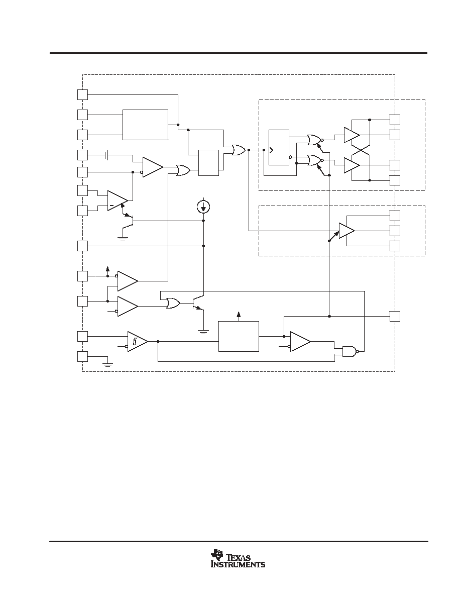
FUNCTIONAL BLOCK DIAGRAM
4
5
6
7
13
11
14
12
CLOCK
RT
CT
RAMP
VC
OUTA
OUTB
PGND
UC28025
3
EAOUT
2
1
8
15
NI
INV
SS
VCC
10
GND
16 VREF
OSCILLATOR
R
PWM
Latch
+
1.25 V
+
Inhibit
1 V
1.4 V
ILIM
Comparator
Shutdown
Comparator
9
ILIM/SD
9 V
UVLO
T
VCC Good
REF GEN
Output Inhibit
VREF Good
4 V
Wide Bandwidth
Error Amplifier
Toggle F/F
Internal Bias
13
14
12
VC
OUT
PGND
UC28023
11
ILIMREF
1 V
(UC28025 Only)
UDG-03048
9
µ
A
V
IN
S
D
(UC28023
Only)