
UC28023
UC28025
SLUS557B - MARCH 2003 - REVISED APRIL 2004
ECONOMY HIGH SPEED PWM CONTROLLER
1
www.ti.com
FEATURES
D
Peak Current Mode, Average Current Mode,
or Voltage Mode (with Feed-Forward) Control
Methods
D
Practical Operation Up to 1 MHz
D
50-ns Propagation Delay to Output
D
±
1.5-A Peak Totem Pole Outputs
D
9-V to 30-V Nominal Operational Voltage
Range
D
Wide Bandwidth Error Amplifier
D
Fully Latched Logic with Double Pulse
Suppression
D
Pulse-by-Pulse Current Limiting
D
Programmable Maximum Duty Cycle Control
D
Under-Voltage Lockout with Hysteresis
D
Trimmed 5.1-V Reference with UVLO
D
Same Functionality as UC3823 and UC3825
APPLICATIONS
D
Off-Line and DC/DC Power Supplies
D
Converters Using Voltage Mode, Peak
Current Mode, or Average Current Mode
Control Methods
D
Single-Ended or Two-Switch Topology
Designs
DESCRIPTION
The UC28023 and UC28025 are fixed-frequency
PWM controllers optimized for high-frequency
switched-mode power supply applications. The
UC28023 is a single output PWM for single-ended
topologies while the UC28025 offers dual
alternating outputs for double-ended and full
bridge topologies.
Targeted for cost effective solutions with minimal
external components, UC2802x include an
oscillator, a temperature compensated reference,
a wide band width error amplifier, a high-speed
current-sense comparator and high-current
active-high totem-pole outputs to directly drive
external MOSFETs.
Protection circuitry includes a current limit
comparator with a 1-V threshold, a TTL
compatible shutdown port, and a soft-start pin
which will double as a maximum duty cycle clamp.
The logic is fully latched to provide jitter free
operation and prohibit multiple pulses at an
output. An undervoltage lockout section with
800
mV of hysteresis assures low start-up
current. During undervoltage lockout, the outputs
are high impedance. Particular care was given to
minimizing propagation delays through the
comparators and logic circuitry while maximizing
bandwidth and slew rate of the error amplifier.
Devices are available in the industrial temperature
range of -40
∞
C to 105
∞
C. Package offerings are
16-pin SOICW (DW), or 16-pin PDIP (N)
packages.
ORDERING INFORMATION
TA = TJ
OUTPUT
EXTERNAL CURRENT
PACKAGED DEVICES
TA = TJ
OUTPUT
CONFIGURATION
EXTERNAL CURRENT
LIMIT REFERENCE
PDIP-16 (N)
SOICW-16 (DW)
- 40
∞
C to 105
∞
C
Single
Yes
UC28023N
UC28023DW
- 40
∞
C to 105
∞
C
Dual Alternating
No
UC28025N
UC28025DW
(1) The DW package are also available taped and reeled. Add an R suffix to the device type (i.e., UC28023DWR (2,000 devices per reel).
PRODUCTION DATA information is current as of publication date.
Products conform to specifications per the terms of Texas Instruments
standard warranty. Production processing does not necessarily include
testing of all parameters.
Copyright
2004, Texas Instruments Incorporated

UC28023
UC28025
SLUS557B - MARCH 2003 - REVISED APRIL 2004
2
www.ti.com
These devices have limited built-in ESD protection. The leads should be shorted together or the device placed in conductive foam
during storage or handling to prevent electrostatic damage to the MOS gates.
ABSOLUTE MAXIMUM RATINGS
over operating free-air temperature range unless otherwise noted(1)
UC28023
UC28025
RATING
UNIT
Input voltage range,
VC, VCC
VC, VCC
30
V
Output current, IOUT(DC)
OUT
OUTA, OUTB
±
0.5
A
Peak output current, pulsed 0.5 ms IOUT(pulsed)
OUT
OUTA, OUTB
±
2.0
A
Capacitive load, CLOAD
200
pF
Analog inputs
INV, NI, RAMP
INV, NI, RAM
-0.3 V to 7 V
A
Analog inputs
SS, ILIM/SD
SS, ILIM/SD
±
2.0
A
Output current, IREF
VREF
VREF
10
Output current, ICLOCK
CLOCK
CLOCK
-5
Soft-start sink current, ISINK_SS
SS
SS
5
mA
Output current, IOUT(EA)
EAOUT
EAOUT
20
mA
Oscillator charging current, IOSC_CHG
RT
RT
-5
Power Dissipation at TA = 25
∞
C (all packages)
1
W
Operating junction temperature range, TJ
-55 to 150
Storage temperature, Tstg
-65 to 150
∞
C
Lead temperature 1,6 mm (1/16 inch) from case for 10 seconds, Tsol
300
C
(1) Stresses beyond those listed under "absolute maximum ratings" may cause permanent damage to the device. These are stress ratings only,
and functional operation of the device at these or any other conditions beyond those indicated under "recommended operating conditions" is
not implied. Exposure to absolute-maximum-rated conditions for extended periods may affect device reliability. All voltages are with respect to
GND. All currents are positive into and negative out of the specified terminal.
1
2
3
4
5
6
7
8
16
15
14
13
12
11
10
9
INV
NI
EAOUT
CLOCK
RT
CT
RAMP
SS
VREF
VCC
OUT
VC
PGND
ILIMREF
GND
ILIM/SD
1
2
3
4
5
6
7
8
16
15
14
13
12
11
10
9
INV
NI
EAOUT
CLOCK
RT
CT
RAMP
SS
VREF
VCC
OUT
VC
PGND
ILIMREF
GND
ILIM/SD
UC28023
N PACKAGE
(TOP VIEW)
UC28023
DW PACKAGE
(TOP VIEW)
UC28025
N PACKAGE
(TOP VIEW)
1
2
3
4
5
6
7
8
16
15
14
13
12
11
10
9
INV
NI
EAOUT
CLOCK
RT
CT
RAMP
SS
VREF
VCC
OUTB
VC
PGND
OUTA
GND
ILIM/SD
1
2
3
4
5
6
7
8
16
15
14
13
12
11
10
9
INV
NI
EAOUT
CLOCK
RT
CT
RAMP
SS
VREF
VCC
OUTB
VC
PGND
OUTA
GND
ILIM/SD
UC28025
DW PACKAGE
(TOP VIEW)

UC28023
UC28025
SLUS557B - MARCH 2003 - REVISED APRIL 2004
3
www.ti.com
ELECTRICAL CHARACTERISTICS
TA = -40
∞
C to 105
∞
C , TJ = TA, RT = 3.65 k
, CT = 1 nF, VCC = 15 V (unless otherwise noted)
PARAMETER
TEST CONDITIONS
MIN
TYP
MAX
UNIT
REFERENCE
VREF
Reference voltage
TJ = 25
∞
C, IREF = 1 mA
5.05
5.10
5.15
V
Line regulation voltage
10 V
VCC
30 V
2
15
mV
Load regulation voltage
1 mA
IREF
10 mA
5
15
mV
Temperature stability(1)
T(min) < TA < T(max)
0.2
0.4
mV/
∞
C
Total output voltage variation(1)
Line, load, temperature
4.95
5.25
V
Output noise voltage(1)
10 Hz < f < 10 kHz
50
µ
V
Long term stability voltage(1)
TJ = 125
∞
C,
1000 hours
5
25
mV
ISS
Short circuit current
VREF = 0 V
-20
-50
-100
mA
OSCILLATOR
fOSC
Initial accuracy(1)
TJ = 25
∞
C
360
400
440
kHz
Voltage stability(1)
10 V
VCC
30 V
0.2%
2.0%
Temperature stability(1)
T(min) < TA < T(max)
5%
Total voltage variation(1)
Line, temperature
340
460
kHz
VCLOCK_H High-level clock output voltage
3.9
4.5
VCLOCK_L Low-level clock output voltage
2.3
2.9
VRAMP(p) Ramp peak voltage(1)
2.6
2.8
3.0
V
VRAMP(v) Ramp valley voltage(1)
0.70
1.00
1.25
V
VRAMP(v-p) Ramp vally-to-peak voltage(1)
1.6
1.8
2.0
ERROR AMPLIFIER
VIN
Input offset voltage
15
mV
IBIAS
Input bias current
0.6
3.0
A
IIN
Input offset current
0.1
1.0
µ
A
AVOL
Open loop gain
1 V
VOUT
4 V
60
95
CMRR
Common mode rejection ratio
1.5 V
VCM
5.5 V
75
95
dB
PSRR
Power supply rejection ratio
10 V
VCC
30 V
85
110
dB
IOUT(sink) Output sink current
V(EAOUT) = 1 V
1.0
2.5
mA
IOUT(src)
Output source current
V(EAOUT) = 4 V
-0.5
-1.3
mA
VOH
High-level output voltage
I(EAOUT) = -0.5 mA
4.0
4.7
5.0
V
VOL
Low-level output voltage
I(EAOUT) = 1 mA
0
0.5
1.0
V
Unity gain bandwidth(1)
3.0
5.5
MHz
Slew rate(1)
6
12
V/
µ
s
PWM COMPARATOR
IBIAS
RAMP bias current
VRAMP = 0 V
-1
-5
µ
A
Maximum duty cycle
UC28023
80%
90%
Maximum duty cycle
UC28025
(2)
40%
45%
Minimum duty cycle
UC28023
0%
Minimum duty cycle
UC28025
0%
EAOUT zero DC threshold
VRAMP = 0 V
1.10
1.25
1.40
V
tDELAY
Delay to output time(1)
50
100
ns
(1) Ensured by design. Not production tested.
(2) Tested as 80% minimum for the oscillator which is the equivalent of 40% for UC28025.

UC28023
UC28025
SLUS557B - MARCH 2003 - REVISED APRIL 2004
4
www.ti.com
ELECTRICAL CHARACTERISTICS
TA = -40
∞
C to 105
∞
C , TJ = TA, RT = 3.65 k
, CT = 1 nF, VCC = 15 V (unless otherwise noted)
PARAMETER
TEST CONDITIONS
MIN
TYP
MAX
UNIT
SOFT-START
ICHG
Charge current
VSS = 0.5 V
3
9
20
µ
A
IDISCHG
Discharge current
VSS = 1.0 V
1.0
7.5
mA
CURRENT LIMIT/SHUTDOWN
ILIMIT
Current limit bias current
0 V < V(ILIM/SD) < 4 V
±
10
µ
A
ILIMIT
Offset voltage
UC28023
15
mV
ILIMREF
Common mode range(1)
UC28023
1.00
1.25
Current limit threshold voltage
UC28025
0.9
1.0
1.1
V
Shutdown threshold voltage
1.25
1.40
1.55
V
tDELAY
Delay to output time(1)
50
80
ns
OUTPUT
VOL
Low-level output voltage
IOUT = 20 mA
0.25
0.40
VOL
Low-level output voltage
IOUT = 200 mA
1.2
2.2
V
VOH
High-level output voltage
IOUT = -20 mA
13.0
13.5
V
VOH
High-level output voltage
IOUT = -200 mA
12
13
Collector leakage
VC = 30 V
100
500
µ
A
Rise time / Fall time(1)
CLOAD = 1 nF
30
60
ns
UNDERVOLTAGE LOCKOUT (UVLO)
Start threshold voltage
8.8
9.2
9.6
V
Hysteresis
0.4
0.8
1.2
V
SUPPLY CURRENT
Start-up current
VCC = 8 V
1.1
2.0
mA
ICC
Operating current
VINV = VRAMP = VILIM = 0 V
VINV = 1 V
25
35
mA
(1) Ensured by design. Not production tested.
THERMAL RESISTANCE
PACKAGE
JA (
∞
C/W)
JC (
∞
C/W)
N(2)
90(2)
45
DW(2)
50-100(2)
27
(2) Specified
JA (junction-to-ambient) is for devices mountied to 5-square-inch FR4 PC board with one ounce copper
where noted. When resistance range is given, lower values are for 5-square-inch aluminum PC board. Test PWB is 0.062
inches thick and typically uses 0.635 mm trace width for power packages and 1.3 mm trace widths for non-power
packages with a 100x100 mil probe land area at the end of each trace.

UC28023
UC28025
SLUS557B - MARCH 2003 - REVISED APRIL 2004
5
www.ti.com
FUNCTIONAL BLOCK DIAGRAM
4
5
6
7
13
11
14
12
CLOCK
RT
CT
RAMP
VC
OUTA
OUTB
PGND
UC28025
3
EAOUT
2
1
8
15
NI
INV
SS
VCC
10
GND
16 VREF
OSCILLATOR
R
PWM
Latch
+
1.25 V
+
Inhibit
1 V
1.4 V
ILIM
Comparator
Shutdown
Comparator
9
ILIM/SD
9 V
UVLO
T
VCC Good
REF GEN
Output Inhibit
VREF Good
4 V
Wide Bandwidth
Error Amplifier
Toggle F/F
Internal Bias
13
14
12
VC
OUT
PGND
UC28023
11
ILIMREF
1 V
(UC28025 Only)
UDG-03048
9
µ
A
V
IN
S
D
(UC28023
Only)

UC28023
UC28025
SLUS557B - MARCH 2003 - REVISED APRIL 2004
6
www.ti.com
TERMINAL FUNCTIONS
NAME
TERMINAL
I/O
DESCRIPTION
NAME
UC28023
UC28025
I/O
DESCRIPTION
CLOCK
4
4
O
Output of the internal oscillator
CT
6
6
I
Timing capacitor connection pin for oscillator frequency programming. The timing capacitor should
be connected to the device ground using minimal trace length.
EAOUT
3
3
O
Output of the error amplifier for compensation
GND
10
10
-
Analog ground return pin.
ILIM/SD
9
9
I
Input to the current limit comparator and the shutdown comparator.
ILIMREF
11
-
I
Pin to set the current limit threshold externally.
INV
1
1
I
Inverting input to the error amplifier
NI
2
2
I
Non-inverting input to the error amplifier
OUT
14
-
O
High current totem pole output of the on-chip drive stage.
OUTA
-
11
O
High current totem pole output A of the on-chip drive stage.
OUTB
-
14
O
High current totem pole output B of the on-chip drive stage.
PGND
12
12
-
Ground return pin for the output driver stage
RAMP
7
7
I
Non-inverting input to the PWM comparator with 1.25-V internal input offset. In voltage mode
operation this serves as the input voltage feed-forward function by using the CT ramp. In peak
current mode operation, this serves as the slope compensation input.
RT
5
5
I
Timing resistor connection pin for oscillator frequency programming
SS
8
8
I
Soft-start input pin which also doubles as the maximum duty cycle clamp.
VC
13
13
-
Power supply pin for the output stage. This pin should be bypassed with a 0.1-
µ
F monolithic
ceramic low ESL capacitor with minimal trace lengths.
VCC
15
15
-
Power supply pin for the device. This pin should be bypassed with a 0.1-
µ
F monolithic ceramic
low ESL capacitor with minimal trace lengths
VREF
16
16
O
5.1-V reference. For stability, the reference should be bypassed with a 0.1-
µ
F monolithic ceramic
low ESL capacitor and minimal trace length to the ground plane.

UC28023
UC28025
SLUS557B - MARCH 2003 - REVISED APRIL 2004
7
www.ti.com
APPLICATION INFORMATION
1
3
4
5
9
7
6
12
ILIM/SD
RAMP
CT
PGND
INV
EAOUT
CLOCK
RT
UC28025
16
2
14
11
OUTB
OUTA
VREF
NI
15
13
VCC
VC
10
8
GND
SS
15 V
22 pF
120 pF
10 nF
1N 5820
150 pF
1 nF
42 V to 56 V
UDG-03047
4.7
µ
F
V
IN
1 k
1 k
1 k
10 k
CT
470 pF
1 k
8.2 k
0.1
µ
F
1.5 k
3.3 k
4.3 k
0.1
µ
F
390
100
4.7
µ
F
4.7
µ
F 12
0.8
µ
H
V
OUT
5 V
1 A to 10 A
6
µ
F
5:1
+
-
-
+
Figure 1. Typical Application: 1.5 MHz, 48-V to 5-V DC/DC Push-Pull Converter Using UC28025

UC28023
UC28025
SLUS557B - MARCH 2003 - REVISED APRIL 2004
8
www.ti.com
APPLICATION INFORMATION
PCB LAYOUT CONSIDERATIONS
High speed circuits demand careful attention to layout and component placement. To assure proper
performance of the UC2802x follow these rules:
1.
Use a ground plane.
2.
Damp or clamp parasitic inductive kick energy from the gate of driven MOSFETs. Do not allow the output
pins to ring below ground. A series gate resistor or a shunt 1-A Schottky diode at the output pin serves this
purpose.
3.
Bypass VCC, VC, and VREF. Use 0.1-
µ
F monolithic ceramic capacitors with low equivalent series
inductance. Allow less than 1-cm of total lead length for each capacitor between the bypassed pin and the
ground plane.
4.
Treat the timing capacitor, C
T
, as a bypass capacitor.
ERROR AMPLIFIER
Figure 2 shows a simplified schematic of the UC2802x error amplifier and Figures 3 and 4 show its
characteristics.
UDG-03049
200
INV
NI
VREF
EAOUT
2
1
16
3
5.1 V
Figure 2. Simplified Error Amplifier Schematic

UC28023
UC28025
SLUS557B - MARCH 2003 - REVISED APRIL 2004
9
www.ti.com
APPLICATION INFORMATION
Figure 3. Open Loop Frequency Response
100
0
-40
1 k
10 k
100 k
1 M
10 M
100 M
-20
60
20
40
80
100
-180
-90
0
GAIN AND PHASE
vs
FREQUENCY
fOSC - Frequency - Hz
A
V
- Gain - dB
Phase -
∞
GAIN
PHASE
3
2
5
4
1
0
0.2
0.4
0.6
0.8
1.0
tdelay - Delay Time-
µ
s
V
SEAout
- E/A Output V
o
ltage - V
Figure 4. Unity Gain Slew Rate
VOLTAGE
vs
TIME
VOUT
VIN
CONTROL METHODS
6
7
CT
UC2802x
OSCILLATOR
1.25 V
RAMP
From
Error Amplifier
Figure 5. Voltage Mode Control
UDG-03050
CT
Figure 6. Peak Current Mode Control
RSENSE
UDG-03050
CT
* A small filter may be required to supress switch noise.
6
7
CT
UC2802x
OSCILLATOR
1.25 V
RAMP
From
Error Amplifier
*
*
ISENSE
UC28023
UC28025
SLUS557B - MARCH 2003 - REVISED APRIL 2004
10
www.ti.com
APPLICATION INFORMATION
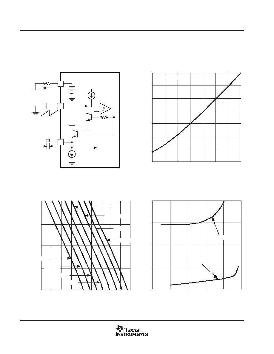
OSCILLATOR
Figure 7. Oscillator Circuit
UDG-03052
6
4
CT
UC2802x
CLOCK
3 V
5
RT
Blanking
5.1 V
IR
IC = IR
TD
400
µ
A
Figure 8.
0.047
0.22
0.047
1.0
2.2
4.7
10.0
22.0
47
0.10
2.20
0.47
1.00
4.70
10.0
100
CT - Timing Capacitance - nF
T
D
- Dead T
ime -
µ
s
DEAD TIME
vs
TIMING CAPACITANCE
3 k
RT
100 k
Figure 9. Oscillator Circuit
10 k
1 k
100 k
1 k
10 k
100 k
1 M
100
10 nF
22 nF
47 nF
100 nF
fOSC - Frequency - Hz
R
T
-
T
iming
Resistance
-
470 pF
1 nF
2.2 nF
4.7 nF
TIMING RESISTANCE
vs
FREQUENCY
Figure 10.
T
D
- Dead T
ime - ns
DEAD TIME
vs
FREQUENCY
160
140
120
100
80
10 k
100 k
1 M
RT = 1 nF
fOSC - Frequency - Hz
RT = 470 pF

UC28023
UC28025
SLUS557B - MARCH 2003 - REVISED APRIL 2004
11
www.ti.com
APPLICATION INFORMATION
SYNCHRONIZATION
Figure 11 shows a generalized synchronization. Figure 12 shows a synchronozed operation of two units in close
proximity.
UDG-03050
4
5
6
CLOCK
RT
CT
UC2802x
(Master)
5
6
RT
CT
UC2802x
(Slave)
Local
Ramp
16
VREF
Local
Ramp
RT
1.15
24
24
CT
43
43
43
CT
RT
10
µ
F
2N222
470
0.1
µ
F
0.1
µ
F
0.1
µ
F
To other
slaves
Figure 11. Generalized Synchronization
Figure 12. Synchronization of Two Units In Close
Proximity
4
5
6
CLOCK
RT
CT
UC2802x
(Master)
4
5
6
CLOCK
RT
CT
UC2802x
(Slave)
16 VREF
Local
Ramp
UDG-03050
RT
CT

UC28023
UC28025
SLUS557B - MARCH 2003 - REVISED APRIL 2004
12
www.ti.com
APPLICATION INFORMATION
FEEDFORWARD CIRCUIT
7
6
5
RAMP
CT
RT
UC2802x
4
CLOCK
CFF
RFF
VIN
UDG-03050
Figure 13. Feedforward Technique for Off-Line Voltage-Mode Applications
CONSTANT VOLT-SECOND CLAMP CIRCUIT
The circuit for the UC28023 shown in Figure 14 describes achievement a constant volt-second product clamp
over varying input voltages. The ramp generator components, R
T
and C
R
are chosen so that the ramp at Pin
9 (ILIM/SD) crosses the 1-V threshold at the same time the desired maximum volt-second product is reached.
The delay through the functional inverter block must be such that the ramp capacitor can be completely
discharged during the minimum deadtime.
14
9
OUT
ILIM/SD
UC28023
CR
RT
VIN
UDG-03050
Figure 14. Achieving Constant Volt-Second Product Clamp with the UC28023

UC28023
UC28025
SLUS557B - MARCH 2003 - REVISED APRIL 2004
13
www.ti.com
The circuit for the UC28025 shown in Figure 15 describes achievement a constant volt-second product clamp
over varying input voltages. The ramp generator components, R
T
and C
R
are chosen so that the ramp at Pin
9 (ILIM/SD) crosses the 1-V threshold at the same time the desired maximum volt-second product is reached.
The delay through the functional inverter block must be such that the ramp capacitor can be completely
discharged during the minimum deadtime.
UDG-03050
14
9
OUTB
ILIM/SD
UC28025
11
CR
RT
OUTA
VIN
Figure 15. Achieving Constant Volt-Second Product Clamp with the UC28025

UC28023
UC28025
SLUS557B - MARCH 2003 - REVISED APRIL 2004
14
www.ti.com
APPLICATION INFORMATION
OUTPUTS
UC28023 has one output and UC28025 has dual alternating outputs.
Figure 16. Simplified Schematic
15 VCC
UC2802x
13 VC
OUTx
12 PWRGND
10 GND
0
0
0.50
0.25
1.00
0.75
1.50
1.25
1
2
3
Figure 17.
IOUT - Output Current - A
V
SA
T
- Saturation V
o
ltage - V
SATURATION VOLTAGE
vs
OUTPUT CURRENT
Source
Sink
Figure 18.
10
0
0.2
40
80
160
200
0
120
5
15
-0.2
0
tRISE (tFALL) - Time - ns
V
OUT
- Output V
o
ltage - V
RISE/FALL TIME
vs
OUTPUT VOLTAGE AND LOAD CURRENT
I LOAD
- Load Current - A
CLOAD =1 nF
Figure 19.
10
0
0.2
100
200
400
500
0
300
5
15
-0.2
0
tRISE (tFALL) - Time - ns
V
OUT
- Output V
oltage - V
RISE/FALL TIME
vs
OUTPUT VOLTAGE AND LOAD CURRENT
I LOAD
- Load Current - A
CLOAD =10 nF

UC28023
UC28025
SLUS557B - MARCH 2003 - REVISED APRIL 2004
15
www.ti.com
APPLICATION INFORMATION
Open Loop Laboratory Test Fixture
The following test fixture is useful for exercising many of the UC28025's functions and measuring their
specifications. As with any wideband circuit, careful ground and by-pass procedures should be followed. The
use of a ground plane is highly recommended.
UDG-03051
200
4
5
6
CLOCK
RT
CT
UC28025
3 EAOUT
7 RAMP
2
1
8
NI
INV
SS
9 ILIM/SD
15
13
11
VCC
VC
OUTA
12
PGND
14
OUTB
10
16
GND
VREF
OSCILLATOR
ERROR
AMPLIFIER
15 V
10 uF
1N5820
1N5820
15 V
0.1
µ
F
10
µ
F
0.1
µ
F
0.1
µ
F
10
µ
F
4.7 k
4.7 k
68 k
27 k
10 k
27 k
22 k
10 k
3.3 k
50
CT 1.0 nF
RT 3.65 k
Figure 20. Laboratory Test Fixture
References
1.
1.5-MHz Current Mode IC Controlled 50-Watt Power Supply, Texas Instruments Application Note Literature
No. SLUA053.
2.
The UC3823A,B and UC3825A,B Enhanced Generation of PWM Controllers, Texas Instruments
Application Note Literature No. SLUA125.


IMPORTANT NOTICE
Texas Instruments Incorporated and its subsidiaries (TI) reserve the right to make corrections, modifications,
enhancements, improvements, and other changes to its products and services at any time and to discontinue
any product or service without notice. Customers should obtain the latest relevant information before placing
orders and should verify that such information is current and complete. All products are sold subject to TI's terms
and conditions of sale supplied at the time of order acknowledgment.
TI warrants performance of its hardware products to the specifications applicable at the time of sale in
accordance with TI's standard warranty. Testing and other quality control techniques are used to the extent TI
deems necessary to support this warranty. Except where mandated by government requirements, testing of all
parameters of each product is not necessarily performed.
TI assumes no liability for applications assistance or customer product design. Customers are responsible for
their products and applications using TI components. To minimize the risks associated with customer products
and applications, customers should provide adequate design and operating safeguards.
TI does not warrant or represent that any license, either express or implied, is granted under any TI patent right,
copyright, mask work right, or other TI intellectual property right relating to any combination, machine, or process
in which TI products or services are used. Information published by TI regarding third-party products or services
does not constitute a license from TI to use such products or services or a warranty or endorsement thereof.
Use of such information may require a license from a third party under the patents or other intellectual property
of the third party, or a license from TI under the patents or other intellectual property of TI.
Reproduction of information in TI data books or data sheets is permissible only if reproduction is without
alteration and is accompanied by all associated warranties, conditions, limitations, and notices. Reproduction
of this information with alteration is an unfair and deceptive business practice. TI is not responsible or liable for
such altered documentation.
Resale of TI products or services with statements different from or beyond the parameters stated by TI for that
product or service voids all express and any implied warranties for the associated TI product or service and
is an unfair and deceptive business practice. TI is not responsible or liable for any such statements.
Following are URLs where you can obtain information on other Texas Instruments products and application
solutions:
Products
Applications
Amplifiers
amplifier.ti.com
Audio
www.ti.com/audio
Data Converters
dataconverter.ti.com
Automotive
www.ti.com/automotive
DSP
dsp.ti.com
Broadband
www.ti.com/broadband
Interface
interface.ti.com
Digital Control
www.ti.com/digitalcontrol
Logic
logic.ti.com
Military
www.ti.com/military
Power Mgmt
power.ti.com
Optical Networking
www.ti.com/opticalnetwork
Microcontrollers
microcontroller.ti.com
Security
www.ti.com/security
Telephony
www.ti.com/telephony
Video & Imaging
www.ti.com/video
Wireless
www.ti.com/wireless
Mailing Address:
Texas Instruments
Post Office Box 655303 Dallas, Texas 75265
Copyright
2004, Texas Instruments Incorporated